
 Open Access Article
 This Open Access Article is licensed under a
 Creative Commons Attribution 3.0 Unported Licence
Understanding metal organic chemical vapour deposition of monolayer WS2: the enhancing role of Au substrate for simple organosulfur precursors†
Ye
Fan‡
 a,
Kenichi
Nakanishi‡
a,
Vlad P.
Veigang-Radulescu
a,
Ryo
Mizuta
a,
J. Callum
Stewart
a,
Jack E. N.
Swallow
b,
Alice E.
Dearle
a,
Oliver J.
Burton
a,
Jack A.
Alexander-Webber
a,
Pilar
Ferrer
c,
Georg
Held
c,
Barry
Brennan
d,
Andrew J.
Pollard
d,
Robert S.
Weatherup
b and
Stephan
Hofmann
*a
a,
Kenichi
Nakanishi‡
a,
Vlad P.
Veigang-Radulescu
a,
Ryo
Mizuta
a,
J. Callum
Stewart
a,
Jack E. N.
Swallow
b,
Alice E.
Dearle
a,
Oliver J.
Burton
a,
Jack A.
Alexander-Webber
a,
Pilar
Ferrer
c,
Georg
Held
c,
Barry
Brennan
d,
Andrew J.
Pollard
d,
Robert S.
Weatherup
b and
Stephan
Hofmann
*a
aElectrical Engineering Division, Department of Engineering, University of Cambridge, UK. E-mail: sh315@cam.ac.uk
bDepartment of Materials, University of Oxford, Parks Road, Oxford OX1 3PH, UK
cDiamond Light Source Ltd, Harwell Science and Innovation Campus, Didcot OX11 0DE, UK
dNational Physical Laboratory, Hampton Rd, Teddington, Middlesex TW11 0LW, UK
First published on 28th October 2020
Abstract
We find that the use of Au substrate allows fast, self-limited WS2 monolayer growth using a simple sequential exposure pattern of low cost, low toxicity precursors, namely tungsten hexacarbonyl and dimethylsulfide (DMS). We use this model reaction system to fingerprint the technologically important metal organic chemical vapour deposition process by operando X-ray photoelectron spectroscopy (XPS) to address the current lack of understanding of the underlying fundamental growth mechanisms for WS2 and related transition metal dichalcogenides. Au effectively promotes the sulfidation of W with simple organosulfides, enabling WS2 growth with low DMS pressure (<1 mbar) and a suppression of carbon contamination of as-grown WS2, which to date has been a major challenge with this precursor chemistry. Full WS2 coverage can be achieved by one exposure cycle of 10 minutes at 700 °C. We discuss our findings in the wider context of previous literature on heterogeneous catalysis, 2D crystal growth, and overlapping process technologies such as atomic layer deposition (ALD) and direct metal conversion, linking to future integrated manufacturing processes for transition metal dichalcogenide layers.
Introduction
Tungsten disulfide (WS2) is a prominent material of the transition metal dichalcogenide (TMDC) family, with a characteristic layered structure of hexagonally packed metal atoms sandwiched between two layers of chalcogen atoms. Monolayer WS2 exhibits a wide direct bandgap (Eg ≈ 2 eV), strong spin–orbit coupling and bright room-temperature photoluminescence (PL).1–4 As a prototypical 2D semiconductor, WS2 has raised promise in applications ranging from (opto-) electronics to spintronics and sensors.1–4 These emergent applications drive the need for scalable growth of atomically thin, highly crystalline “electronic-grade” 2D layers/films,5 which is distinct from the historic focus on TMDC bulk crystal growth,6 and from classic TMDC application areas such as lubricants or catalysis.7 A large body of recent literature highlights the progress in such “electronic-grade” TMDC layer growth.5 However, the vast parameter space and increased complexity in structure and possible mechanisms, when compared to graphene for instance, leaves the understanding of even the basic processes of TMDC layer growth still severely limited.The currently most prevalent TMDC growth method employs powder vaporisation, typically based on the sublimation of solid precursors in a hot wall reactor, and has demonstrated large monolayer TMDC crystal domains (>100 μm) on inert substrates like SiO2/Si,8 and sapphire,9 as well as on metals such Ni–Ga alloys10 and Au.11,12 For the latter, growth has been referred to as catalytic,11 analogous to graphene and nanowire growth.13,14 However, the growth atmosphere is difficult to accurately control and modulate, which restricts uniformity and scalability as well as makes such powder based techniques too complex, as model systems, to advance the required fundamental understanding of crystal growth. Driven by the need for low-cost, high through-put and industrial compatibility, metal–organic chemical vapour deposition (MOCVD) and related atomic layer deposition (ALD) type techniques have emerged as prime candidates for integrated manufacturing of electronic-grade TMDC layers.5,15 MOCVD of WS2 thin films with average domain sizes of the order of micrometres has been demonstrated on insulating amorphous and crystalline substrates including SiO2/Si and c-plane sapphire, yet the understanding of the underlying growth mechanisms and thus how to control the layer microstructure is still in its infancy.16,17 Reported MOCVD growth times for monolayer WS2 are often on the order of one to tens of hours for complete coverage.18–20
Carbon contamination introduced by organic precursors is a major challenge for MOCVD, and a range of metal and chalcogen precursors have been explored to address this challenge for TMDCs.19,20 Such optimisation often results in a choice of precursors that are toxic and/or difficult to handle. While standard MOCVD is based on the co-exposure of the constituent precursors, sequential exposure patterns like for ALD have also been explored.21–23 However, in contrast to standard 3D materials, for TMDCs such choice of sequential exposure is less obvious, since layer-by-layer growth for 2D materials is largely dictated by their anisotropic layered crystal structure. ALD-type approaches to date have shown limited TMDC layer control and not perfect crystallinity (grain/cluster sizes <20 nm).24–26 The same also typically holds for ‘direct conversion’ approaches, where the metal is, for example, deposited by physical vapour deposition and then exposed to chalcogenide precursors.27–29 A range of hybrid approaches tailored to optimise 2D TMDC growth, for example by post annealing,30 are also emerging. In terms of understanding mechanisms, there is parallel to heterogeneous catalysis, such as hydrotreating processes like hydro-desulfurization (HDS), for which the formation of metal sulfide and the active edge and defect sites of nanoparticulate TMDC catalysts have been explored in many detailed surface science studies.31–33 Such studies have also been extended to molecular beam epitaxy (MBE) and other ultra-high vacuum techniques for TMDC growth and van der Waals epitaxy.34–36
We here focus on a “deconstructed” MOCVD process for WS2, based on a simple sequential exposure pattern of low cost, low toxicity precursors, namely tungsten hexacarbonyl [THC; W(CO)6] and dimethyl sulfide [DMS; S(CH3)2]. This sequential exposure pattern, combined with cold wall reactor use, minimises precursor pre-reactions and promotes a substrate surface bound reaction path. It also enables us to explore the entire WS2 growth process by operando X-ray photoelectron spectroscopy (XPS) in order to develop a more detailed understanding. We employ this model system to explore the effects of using a metal substrate for such MOCVD process, specifically Au. Au forms no stable compounds with either W or S in bulk form, W or S solubilities in solid Au are not significant,37 and Au(111) has been widely used in surface science studies of TMDC growth.31,32 Sulfidation with organosulfides like DMS or dimethyl disulfide (DMDS), compared to H2S, is known to result in catalysts with a higher intrinsic HDS reactivity, whereby the effective chemical potential of sulfur is lowest for DMS,38 and found to affect the size and morphology of the resulting TMDC nanoclusters.39 No evidence has been found for the existence of surface or bulk carbide phases in HDS catalysts and simulations highlight that substitution of sulfur with carbon in MoS2 nanoparticles is unfavourable.39 There is a large body of literature on the absorption of thiols or disulfides onto Au, forming self-assembled monolayers, including reports of dissociation of organosulfides on Au.40–42 This motivates us here to explore the use of Au in conjunction with DMS as sulfidation agent for MOCVD of WS2 layer growth. We find that the Au substrate allows a significant reduction in the DMS pressure required to nucleate and grow WS2 by MOCVD. The simple reaction scheme exhibits a self-limiting behaviour to monolayer WS2, and full coverage can be achieved by one exposure cycle of 10 minutes in total. We find the low DMS pressure also leads to a significant reduction in the carbon contamination present in as-grown WS2. We discuss our results and insights into the growth process in the context of the diverse prior literature.
Results and discussion
The MOCVD process is ‘deconstructed’ into 2 steps with sequential exposure of metal and chalcogenide precursors as schematically highlighted in Fig. 1. Poly-crystalline Au foil (25 μm thick; Alfa Aesar) is used as the growth substrate and is annealed and plasma cleaned prior to being loaded into the MOCVD reaction chamber (Fig. 1(b, i)). The grain size of Au is around 100 μm. For ex situ experiments, a custom-built cold wall reactor (base pressure of 2.5 × 10⁻⁶ mbar) is used with remote sample heating via an IR laser (see Methods). Laser heating enables a low thermal mass for fast ramping and quenching, while at the same time minimizes cross-contamination. For operando XPS we employed an environmental reaction chamber with resistive heating (see Methods). The sample is initially held in vacuum at growth temperature to desorb surface contaminants and stabilize growth conditions (Fig. 1(b, ii)), followed by a low pressure (5 × 10⁻⁶ mbar) THC exposure, which we refer to as “metallization” (Fig. 1(b, iii)). THC is a well-studied precursor for W film deposition that readily decomposes at 700 °C particularly on metallic surfaces.43 The second-growth step is a DMS exposure, which we refer to as “sulfidation” (Fig. 1(b, iv)). For a sub-set of experiments the sample was quenched to below 250 °C within 30 s after metallisation, before being heated back to 700 °C for the sulfidation, in order to completely decouple the process steps. However, we find that such quenching does not affect the growth outcome for the given set-ups and probed parameter space in comparison to isothermal processing at 700 °C, as indicated in Fig. 1. We find the sulfidation will happen fast enough to result in continuous WS2 films with DMS pressures as low as 0.1 mbar (Fig. 2). This parameter choice was thus adopted for the operando XPS experiments (Fig. 3). A full characterization of WS2 grown with DMS pressures varied between 0.03 and 1 mbar is presented in Fig. 5 with focus on the carbon contamination.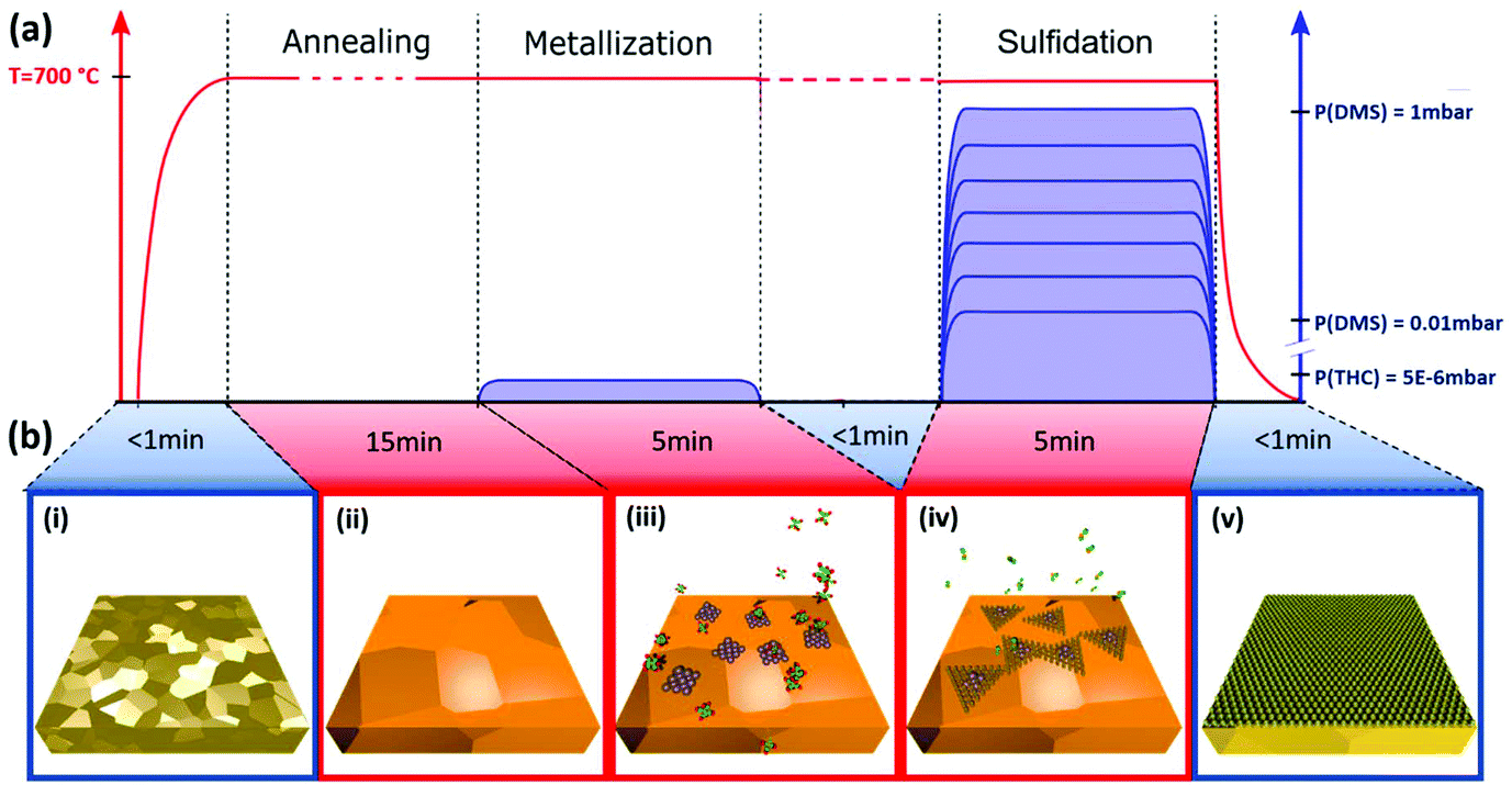 | ||
| Fig. 1 (a) Schematic of ‘deconstructed’ MOCVD procedure: Au substrate is heated up to growth temperature in vacuum, followed by exposure to THC, referred to as metallisation, and separate exposure to DMS, referred to as sulfidation. (b) Schematic of basic processes: Au foil before loading to reaction chamber (i), grain growth of Au (ii), W deposition (iii), WS2 nucleation (iv) and domain growth into monolayer WS2 film (v). | ||
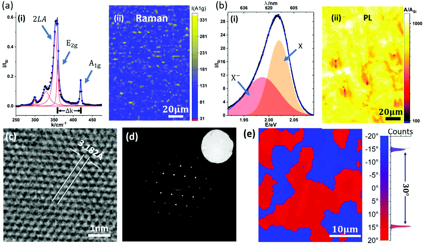 | ||
| Fig. 2 Characterizations of MOCVD WS2 film. (a) Raman spectroscopy of WS2 film transferred onto SiO2/Si. (i) Typical Raman spectrum normalized by the Raman peak of Si. Measurement data (black dots) overlaps well with the fitted curve (blue). Some major modes (2LA, E2g and A1g) among all the Raman peaks (red) are labelled. (ii) Raman mapping of A1g peak height. (b) PL characterization of WS2 film transferred on SiO2/Si substrate. (i) Typical PL spectrum normalized by the Raman peak of Si. Measurement data (black dots) overlap well with the fitted curve (blue). The exciton (X) and trion (X−) peaks are labelled. (ii) Integrated PL intensity mapping normalized by the integrated Raman intensity of Si. (c) HRTEM of the WS2 film. Lattice constant is measured as ∼3.2 Å. (d) SAED of WS2 film. The sharp 6-fold diffraction pattern indicates good crystallinity. The inset shows bright field TEM image of the SA. (e) TEM diffraction mapping of WS2 film. The average grain size of WS2 of the mapped area is around 10 μm, with a bimodal crystal orientation with 30° rotation (FWHM < 1°). | ||
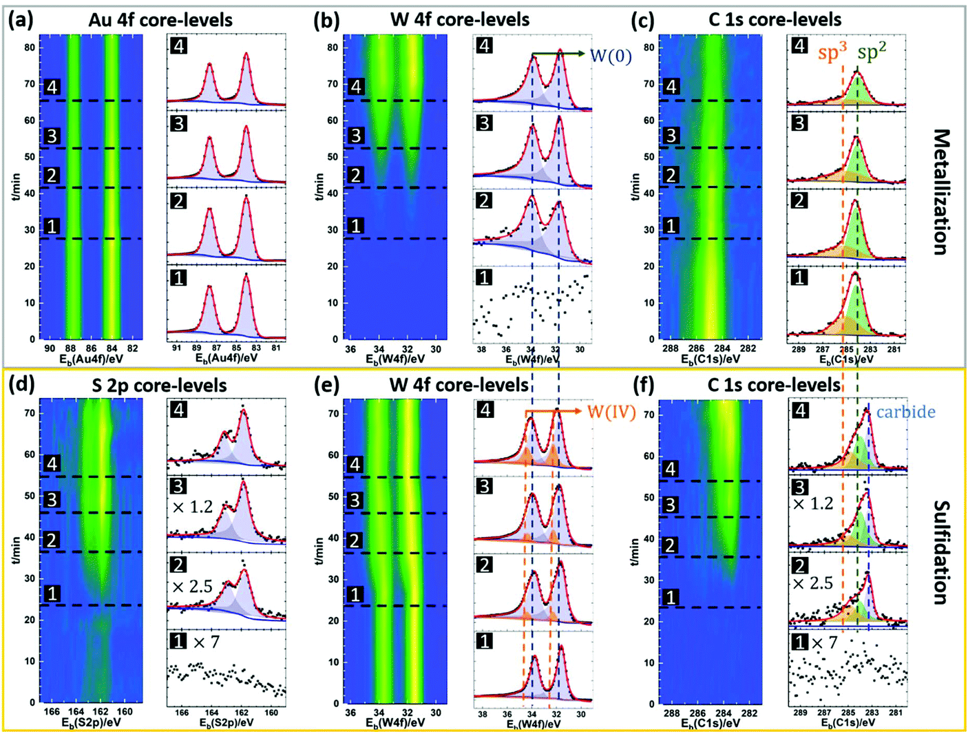 | ||
| Fig. 3 Operando XPS of the MOCVD process. (a)–(c) Time-resolved Au 4f, W 4f and C 1s core-level spectra, respectively, during metallisation step. (d)–(f) Time-resolved S 2p, W 4f and C 1s core-level spectra, respectively, during the sulfidation step. From (a) to (f), the XPS intensity map over reaction time is presented on the left, while the selected spectra of each element showing different reaction stages are presented on the right. | ||
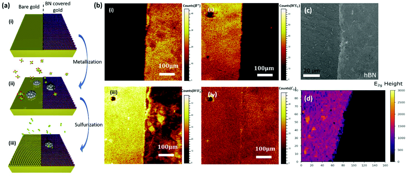 | ||
| Fig. 4 WS2 growth on Au partially covered by monolayer hBN. (a) Schematic of sample (i) and MOCVD procedure with metallisation (ii) and sulfidation (iii). (b) Select ToF-SIMS surface images of the sample after complete MOCVD process: (i) B+ image highlighting hBN coverage; (ii) WS3− image highlighting WS2 coverage; (iii) WO3− image to characterize W coverage; (iv) C2− image to characterize residual carbon. (c) SEM image of sample. No WS2 is found to grow on hBN covered Au. (d) Raman intensity map of sample. E2g height is mapped near the edge of hBN after MOCVD of WS2. | ||
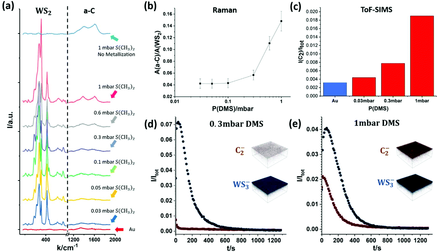 | ||
| Fig. 5 Carbon contamination introduced during sulfidation step: (a) Raman spectra of samples grown at different DMS pressures. For reference, the Raman spectra of as-annealed Au foil (red curve, bottom) and Au foil with only sulfidation at 1 mbar (light blue curve, top), but without metallization, are also included. (b) Integrated Raman peak intensity ratio between amorphous carbon (a-C) and WS2vs. DMS pressure during sulfidation. The error bar is 5 times of the variation in each measurement. (c) Normalized ToF-SIMS C2− ion intensity vs. DMS pressure during sulfidation. For reference, measurement on as-annealed Au foil is also included. (d and e) ToF-SIMS depth profile and 150 μm × 150 μm 3D depth profile images for C2− and WS3− ions for a WS2 monolayer grown on Au foil comparing low (0.3 mbar, (d)) and high (1 mbar, (e)) DMS pressures during sulfidation. Both carbon and WS2 uniformly distribute over the 150 μm × 150 μm region of measurement. | ||
Fig. 2 shows the characterization of a WS2 film grown by our deconstructed MOCVD process with 0.1 mbar DMS during the sulfidation step. The WS2 layer is transferred onto a SiO2/Si wafer support for Raman and photoluminescence (PL) measurements, and Quantifoil support for TEM. Fig. 2(a, i) shows a representative Raman spectrum of the WS2 with E2g and A1g vibration modes measured at 356.9 cm−1 and 417.6 cm−1, respectively, and with a full-width-half-maximum (FWHM) of 4.3 cm−1 and 4.2 cm−1, respectively. This is in line with previously reported Raman measurements using 532 nm laser excitation for WS2 transferred onto SiO2.44–46Fig. 2(a, ii) shows a map of A1g peak height over 108 μm × 154 μm area, which confirms the continuity of the as-transferred WS2 layer. The monolayer nature of as-grown WS2 is further confirmed by the strong PL peak with an exciton energy of ∼2.02 eV (Fig. 2(b, i)). Fig. 2(b, ii) shows a map of normalized integrated PL intensity over the same area as the Raman mapping in Fig. 2(a, ii). Despite some fluctuations, the PL intensity of WS2 film is always orders of magnitudes stronger than the Si Raman signal (also stronger than the WS2 Raman signal), consistent with the monolayer character of the WS2 and the absence of WS2 multi-layer regions.3 Similar to previous reports on CVD/MOCVD WS2, a significant trion peak around 1.98 eV is detectable.47
Fig. 2(c)–(e) show high resolution transmission electron microscope (HRTEM) images and diffraction mapping results for a transferred WS2 film. The representative HRTEM image in Fig. 2(c) highlights the crystallinity of the WS2, confirming a hexagonal lattice structure. The lattice constant is approximately 3.18 Å, which is consistent with both theory,48,49 and previously reported measurement results.50,51 The selected-area electron diffraction (SAED) analysis in Fig. 2(d) shows a matching clear hexagonal diffraction pattern with sharp spots. In order to determine the crystal orientation over a reasonably large area, over 200 diffraction patterns across a 40 μm × 40 μm WS2 film area were taken to construct the map shown in Fig. 2(e). We find two dominating crystal orientations rotated by 30°±1° as highlighted by the bimodal distribution (Fig. 2(e)). Although the influence of crystal orientation of the Au to the crystal orientation of WS2 is not our focus in this report, we are aware of the possible heterogeneity in WS2 arising from the poly-crystallinity of the Au substrate. The data indicates, however, an average WS2 grain size of the order of 10 μm, which compares favourably to previous literature on MOCVD TMDC materials on non-catalytic substrates with typical domain sizes on the order of a few micrometres.20 The representative transfer curve of a two-terminal WS2 field effect transistor (FET) device structure is shown in Fig. S3 in ESI† with a positive light response. The MOCVD WS2 shows n-type behaviour with a field-effect mobility of approximately 0.5 cm2 V−1 s−1, which is comparable to previously reported values.11,52
In this paper, we focus on providing insight into the reactions during the ‘deconstructed’ MOCVD process and identifying the key parameters for WS2 crystal growth control. Fig. 3 shows time-resolved operando XPS of the metallization and sulfidation steps. Fig. 3(a)–(c) show the Au 4f, W 4f and C 1s core level data during the metallization step. In Fig. 3(a), the Au 4f7/2 core level energy is fixed to 84.0 eV allowing calibration of the other spectra. The peak position of the Au 4f5/2 was 87.7 eV, consistent with a spin–orbit splitting of 3.7 eV.53 During the metallization process, the intensities of the Au 4f peaks decrease over time, while the intensities of W 4f peaks increase, (Fig. 3(a) and (b)) indicating the deposition of W onto the Au surface. The binding energies (BEs) of the W 4f doublet are measured at ∼31.5 eV and ∼33.7 eV for the W 4f7/2 and W 4f5/2, respectively. The long-tail character of the W doublet peaks are fitted well by Doniach–Šunjić (DS) line-shapes, which confirms that the deposited tungsten is metallic.54 We note that a W 5p3/2 component is expected around 5.5 eV to 6 eV above the W 4f7/2, but is of insufficient intensity to be resolved above the tail. To rule out the formation of tungsten carbide, the C 1s core-level is measured during the metallization process. The broad peaks at 284.2 eV (assigned to sp2 carbon) and at 285.3 eV (assigned to sp3 carbon) can be detected prior to exposure as shown in Fig. 3(c), consistent with amorphous carbon (a-C) species.55 The C 1s peak associated with tungsten carbide is expected to have a distinctly lower BE (∼283.3 eV) than what is measured during the metallization process, indicating an absence of tungsten carbide at this stage.56 Additionally, during THC exposure the intensity of the C 1s peak decreases without significant change in shape or position of the peak, indicating that the carbon comes from initial Au surface contamination, rather than being introduced by THC dissociation.
Fig. 3(d)–(f) shows the S 2p, W 4f and C 1s core level spectra during the sulfidation step. The formation of WS2 is marked by an increase in S 2p doublet peak intensity with the BEs of 161.8 eV (S 2p3/2) and 163.0 eV (S 2p1/2), respectively. These BEs agree with previously reported values for WS2.57 The conversion of W to WS2 is also marked by the shift and broadening of the W 4f lines during sulfidation, as shown in Fig. 3(e) and Fig. S5 in ESI.† W core level signatures from both metallic tungsten and WS2 are observable during sulfidation. The W 4f peaks for WS2 are measured at 32.2 eV for W 4f7/2 and 34.4 eV for W 4f5/2, with their intensities increasing during DMS exposure, as shown in Fig. 3(e). It is interesting to note that only a fraction of W transforms into WS2 even for extended DMS exposure (Fig. 3(e)). This indicates the self-limiting nature of the tungsten sulfidation reaction on the surface of Au. Since the W 4f peaks for metallic tungsten overlap strongly with those for carbide,53 we do not separate them when fitting the W 4f signals. The metal carbide and other carbon contamination in as-grown WS2 is monitored by the C 1s signal (Fig. 3(f)), which clearly increases during sulfidation. We notice a significant C 1s core level signal around 283.3 eV, in addition to the two peaks attributed to a-C in Fig. 3(c). We assign this to tungsten carbide with a distinctively lower BE. This indicates the formation of metal carbide as a side reaction and confirms DMS as the source of carbon contamination for the WS2 MOCVD process studied here. Although the sulfidation of W is self-limiting, the deposition of a-C contamination proceeds with ongoing DMS exposure (ESI, Fig. S4†).
To further study the role of the Au surface in the MOCVD process, we compare the growth result of WS2 on bare Au to that on monolayer hexagonal boron nitride (hBN) covered Au (Fig. 4). The motivation thereby is for the hBN to suppress direct gas precursor contact with the Au surface. hBN has been used as growth substrate in previous reports and is known remain intact after the MOCVD reaction.58 We also expect hBN to affect adatom mobilities. Monolayer hBN was grown by CVD on Pt and transferred onto the Au using PMMA.59 Post-growth ToF-SIMS imaging is used to map the growth results, as shown in Fig. 4(b). Fig. 4(b, i) shows a 500 μm × 500 μm map of the detected B+ ion species, that act as a fingerprint for the presence of the hBN film. The B+ map indicates continuous hBN coverage on Au after WS2 growth and confirms that the hBN film remains intact throughout the MOCVD process. Fig. 4(b, ii) shows a map of the detected WS3− ion species, used to fingerprint the presence of WS2. We find that a WS2 film only forms on the Au surface without hBN coverage. The unreacted W will be oxidized in air at the post-growth stage, so tracking the location of the WO3− ion species enables us to separate the signals of unreacted W and WS2, as shown in Fig. 4(b, iii). W is found on both the hBN covered and uncovered Au surface. This is consistent with the high chemical reactivity of the THC precursor and its ready thermal decomposition at the metallisation temperature.43 The more sporadic W coverage on the hBN can be due to increased desorption and/or increased W adatom mobility. To rule out the influence of polymer residues on the hBN to the decomposition of DMS, Fig. 2(b, iv) presents a map of the detected C2− ion species on the surface as a fingerprint for such carbon contamination. No difference in the average carbon level between the hBN covered and uncovered Au surface is observed. We thus rule out polymer residuals as a cause of the different WS2 growth behaviour on Au and hBN covered Au. Moreover, this result also highlights that although the sulfidation rate is promoted by Au, side reactions such as the formation of carbides (see Fig. 3f) are similar on the different substrates.
Fig. 5 shows Raman spectroscopy and ToF-SIMS data, highlighting the influence of DMS partial pressures during sulfidation on the carbon contamination of as-grown WS2 on Au. Fig. 5(a) plots the intensity of characteristic Raman peaks for WS2 and a-C for DMS pressures from 0.03 mbar to 1 mbar during sulfidation. For comparison, Fig. 5(a) also shows the spectra for plain, annealed Au foil (red curve, bottom) and Au foil that has undergone only sulfidation (without prior metallization) at 1 mbar (light blue curve, top). The data shows that the a-C Raman peak intensities increase with increasing partial pressures of DMS. Furthermore, Fig. 5(b) plots the integrated Raman peak intensity of a-C (from 1100 cm−1 to 1900 cm−1) normalized by the integrated peak intensity of WS2 (from 250 cm−1 to 500 cm−1). This highlights that the carbon contamination increases greatly past 0.3 mbar DMS pressure during sulfidation, which is consistent with previous literature regarding the strong contamination from DMS in MOCVD TMDC growth in the millibar pressure range.20
In order to further confirm the correlation between DMS partial pressure and carbon contamination, we employ ToF-SIMS depth profiling with a very gentle sputter rate to measure the chemical environment of monolayer WS2 on the Au surface. The depth profiles of carbon and WS2 are summarized in Fig. 5(c)–(e). Among the many carbon species detectable due to the complex decomposition of DMS, we find the C2− ion signal to be the most intense, and hence employ here the C2− ion signal as an indicator of carbon contamination. In Fig. 5(c) the C2− ion intensity for an as-annealed Au foil is additionally added to reference for the level of absorbed carbon contamination due to sample transfer in air. The ToF-SIMS data (Fig. 5(c)) confirms the trend seen in the Raman spectroscopy data (Fig. 5(b)) with the carbon concentration increasing with DMS partial pressure. Fig. 5(d) and (e) also show representative ToF-SIMS 3D depth profile images of fully grown WS2 monolayers on Au foil comparing low (0.3 mbar, Fig. 5(d)) and high (1 mbar, Fig. 5(e)) DMS pressures during sulfidation. The depth profiles are normalized with respect to total ion count to allow direct comparison (see Methods). The 3D ion image insets show that for both samples the C2− and WS3− ion intensities are uniform laterally across the measured 150 μm × 150 μm area. However, the C2− ion intensity on the Au surface is significantly higher for the sample sulfidized in 1 mbar DMS. Regarding the depth dependence, the ToF-SIMS depth profiles show that for the sample grown with a low partial pressure of DMS the carbon contamination only appears on the very surface and quickly diminishes when probing further into the WS2 layer and Au (Fig. 5(d)). In contrast, for a high partial pressure of DMS, a much higher C2− ion intensity is detected on and away from the surface, indicating a heavier carbon contamination of the as-grown WS2. This is further evidenced by the 2 mm × 2 mm surface images of the samples shown in Fig. S2 in ESI,† confirming an elevated carbon signal on the surface of the sample with high (1 mbar) DMS partial pressure.
Our simple, “deconstructed” MOCVD process allows a ‘first-order’ growth model to be developed that provides a framework for rational future process design and sets the foundation for exploring more detailed effects such as the influence of Au surface orientation. Our operando XPS data shows that the THC exposure leads to metallic W deposition on the Au surface. Our ToF-SIMS shows negligible levels of W and S in the post-growth Au bulk (see ESI, Fig. S1 and S2†), consistent with reported bulk phase diagrams.37 Monolayer WS2 growth occurs at isothermal conditions, with no further growth or precipitation of W or S during cooling (Fig. 3). Bulk dissolution effects are not significant to such WS2 growth. Extended THC exposure, i.e. more W deposition, does not lead to multi-layer WS2 growth. Rather, we observe an increasing number of particles (see ESI, Fig. S6†) in addition to the WS2 monolayer. Previous STM work on epitaxial MoS2 nucleation on Au(111) highlights the presence of amorphous Mo clusters as a result of insufficient sulfidation.32 In analogy we propose excess W as the source of the observed particles here. This is consistent with the SIMS mapping in Fig. 4 showing W clusters on hBN covered Au. Since W can be detected on both hBN covered Au and bare Au, we determine that the THC decomposition is not surface selective in our reaction conditions. The W clustering indicates a reasonably high W surface mobility, which is required to achieve large WS2 crystal domain sizes. We observe no W sulfidation on top of the hBN (Fig. 4). Further, we note that as the tungsten thickness is increased the sulfidation to WS2 at the same conditions becomes less complete, and for W foil (∼25 μm), we can detect no 2D WS2 by Raman after sulfidation. This clearly highlights the role of the exposed Au surface in promoting sulfidation of W by DMS to form WS2. In contrast to H2S, which has been shown to promote metal sulfidation on top of an existing TMDC layer, thereby leading to multi-layer TMDC growth,32 DMS presents a lower effective sulfur chemical potential, consistent with the lower TMDC growth rates that have been observed compared to when H2S is used.38 For our sulfidation process Au allows a significant lowering of the partial pressure of the DMS while still enabling high WS2 growth rates so that full coverage can be achieved with <10 min sulfidation cycles. Importantly, WS2 growth in our process is “self-limited” to monolayer thickness. This can be rationalised with the known high affinity of Au for organosulfide adsorption leading to selectively enhanced concentrations on the Au surface.42 In turn, less efficient chemisorption and high precursor desorption can be expected for inert surfaces like hBN. Thus, with the lower effective sulfur chemical potential of DMS, the supersaturation required for WS2 nucleation is only satisfied on the Au surface in our reaction conditions. Once a layer of WS2 grows and covers the Au, it prevents the DMS molecules from reaching the Au, similar to the hBN layer in Fig. 4. This leads to the observed self-limiting WS2 growth behaviour.
Thermal decomposition of DMS is reported to be slow and incomplete at our reaction temperature of 700 °C.60,61 The relatively fast WS2 growth time that we observe is indicative of a clear enhancing effect of the metallic Au surface for the sulfidation with DMS. This is consistent with the known strong chemisorption of organosulfides on Au and their favourable dissociation on Au reported in heterogeneous catalysis literature.40–42 There are a range of possible competing reactions including W carbide formation.62 Our operando XPS data highlights that although the sulfidation of W is self-limiting, the deposition of a-C contamination and formation of tungsten carbide proceeds with ongoing DMS exposure (Fig. 3). This is consistent with excess W being present on top of the formed WS2 layer, similar to excess Mo clusters reported in previous STM work on top of formed MoS2 layers on Au.32 It appears that without direct contact to Au, the DMS exposure of excess W results in a different reaction pathway dominated by carbide/surface carbon formation. The result of DMS exposure of W clusters will further depend on their support, as indicated by the different behaviour on hBN (Fig. 4).
Conclusions
We use a deconstructed MOCVD model process to understand the detailed chemical reaction during MOCVD process and discover the significant enhancing role of Au on the sulfidation step, which results WS2 monolayer growth with a simple organosulfide like DMS. This opens the possibility of using less-toxic precursors for MOCVD and ALD-type reactions, while achieving low carbon contamination and fast growth times. The much lower chalcogen precursor pressure not only yields self-limiting monolayer WS2 growth but also makes the overall process much more efficient and gives wider compatibility with standard growth reactors. The reaction scheme also opens future operando process characterisation opportunities, to further progress the understanding of the underlying mechanisms. Operando characterisation has been crucial to advancing the understanding and thus control of graphene and hBN film growth,13 and we expect our results and the growth model presented here to form the basis for more detailed understanding of TMDC MOCVD. In analogy to catalytic graphene growth on Pt, this will include metal surface orientation dependent growth kinetics, and links to the challenge of cost-efficient and scalable metal substrate preparation.63,66 While we here focus on Au, which requires subsequent WS2 transfer for typical opto-electronic device applications, our findings also motivate further studies on catalytic enhancement of dielectric support films, which would allow direct, transfer-free device integration. In contrast, for electro-chemical applications TMDC layers grown directly on Au can serve as powerful model system for new approaches to catalyst design.Methods
‘Deconstructed’ MOCVD growth of WS2 on Au
25 μm Au foils with 99.985% purity from Alfa Aesar were used as the growth substrates. All as-received Au substrates were annealed for 6 hours at 1025 °C under total pressure of 800 mbar with H2![[thin space (1/6-em)]](https://www.rsc.org/images/entities/char_2009.gif) :Ar = 1:9. Right before the growth, samples were treated by oxygen RIE (150 mTorr, 50 W, 5 min) to remove surface carbon contamination. All ex situ MOCVD growth was carried out in a cold-wall low pressure MOCVD furnace. An 808 nm continuous wave (CW) IR laser was used for sample heating. Sample temperature during growth was monitored by 1.6 μm IR pyrometer assuming transmission 0.9 and emissivity 0.2. The temperature measurement error was estimated as ∼50 °C. In all experiments, the samples were heated to 700 °C under base pressure better than 3 × 10⁻⁶ mbar for 15 min to anneal and stabilize the system. After the annealing, W(CO)6 (99.9%+ purity from Strem Chemicals) was sublimed at 120 °C and fed into the system as the W precursor during metallization. The partial pressure of W(CO)6 was controlled by leak-valve, which allow a pressure control precision better than 5 × 10⁻⁷ mbar. During the metallization, 5 × 10⁻⁶ mbar W(CO)6 was introduced to the chamber and exposed to Au foil at 700 °C for 5 min. After this, 5.5 × 10⁻³ mbar Ar is introduced to stabilize the base pressure when S(CH3)2 (99%+ purity from Sigma Aldrich) was fed into the system as S precursor during sulfidation. The partial pressure of S(CH3)2 was also controlled by a leak-valve. S(CH3)2 with controlled partial pressure ranging from 0.01 mbar to 1 mbar was introduced for the sulfidation of different samples to compare its influence on WS2 produced. After sulfidation, the sample is cooled down rapidly for further characterization.
:Ar = 1:9. Right before the growth, samples were treated by oxygen RIE (150 mTorr, 50 W, 5 min) to remove surface carbon contamination. All ex situ MOCVD growth was carried out in a cold-wall low pressure MOCVD furnace. An 808 nm continuous wave (CW) IR laser was used for sample heating. Sample temperature during growth was monitored by 1.6 μm IR pyrometer assuming transmission 0.9 and emissivity 0.2. The temperature measurement error was estimated as ∼50 °C. In all experiments, the samples were heated to 700 °C under base pressure better than 3 × 10⁻⁶ mbar for 15 min to anneal and stabilize the system. After the annealing, W(CO)6 (99.9%+ purity from Strem Chemicals) was sublimed at 120 °C and fed into the system as the W precursor during metallization. The partial pressure of W(CO)6 was controlled by leak-valve, which allow a pressure control precision better than 5 × 10⁻⁷ mbar. During the metallization, 5 × 10⁻⁶ mbar W(CO)6 was introduced to the chamber and exposed to Au foil at 700 °C for 5 min. After this, 5.5 × 10⁻³ mbar Ar is introduced to stabilize the base pressure when S(CH3)2 (99%+ purity from Sigma Aldrich) was fed into the system as S precursor during sulfidation. The partial pressure of S(CH3)2 was also controlled by a leak-valve. S(CH3)2 with controlled partial pressure ranging from 0.01 mbar to 1 mbar was introduced for the sulfidation of different samples to compare its influence on WS2 produced. After sulfidation, the sample is cooled down rapidly for further characterization.
CVD/transfer of hBN
hBN was grown on 25 μm thick platinum (Pt) foils (99.99%, Alfa Aesar) on a 0.5 mm tantalum (Ta) foil support as previously reported.59 Prior to loading, the Pt foils were cleaned by sonication in acetone followed by iso-propanol and dried with a nitrogen gun. The growth recipe consisted of heating the sample in base pressure ∼2 × 10⁻⁶ mbar to 1000 °C then annealing at temperature for 5 minutes. Subsequently, 1 × 10⁻⁵ mbar partial pressure of borazine (>97%, Fluorochem) was dosed into the chamber via a manually operated leak valve to initiate isothermal growth for 5 minutes. A continuous monolayer BN is produced on Pt by this method. The sample was rapidly cooled under borazine atmosphere.Electrical delamination, or ‘bubbling’, transfer of hBN is used to peel BN off from Pt.64 PMMA (A4, 950k) was spun on the as grown hBN on Pt at 3000 rpm for 45 s as the scaffold layer. PMMA/BN is then peeled off from the Pt by hydrogen bubbling generated by the electrolysis of water in 0.2 M Na(OH) (aq.). The film is then rinsed and fished up by a piece of Au foil to cover half of the surface. After drying overnight, the Au piece with semi-coverage of PMMA/BN is heated to 180 °C for 30 min to soften the PMMA then soaked in acetone to remove the PMMA scaffold.
Transfer of WS2 on Au by wet etching
PMMA (A4, 950k) was spun on the as grown WS2 on gold at 3000 rpm for 45 s. The sample is then baked at 120 °C for 3 min to evaporate the solvent of polymer. WS2 covering the backside of gold is removed by 50 W, 20 s reactive ion etching (RIE) in 150 mTorr CF4. After the RIE, gold is etched by KI/I2 based gold etchant (Sigma-Aldrich) within 4 hours. The sample is then scooped out and rinsed in DI water for several times before being fished out by the target substrate and dried.Raman/PL
Both Raman and PL spectra of samples are taken by a Renishaw invia Raman system. The excitation laser is 20 mW, 532 nm. Single spot Raman is measured with 1% laser power 2 s exposure and accumulated 6 times. For Raman mapping, 10% laser power, 0.1 s exposure is used for each spot with a step size of 2 μm in both x and y direction. Single spot PL is measured by 0.1% laser power 1 s exposure and accumulated 2 times. For PL mapping, 1% laser power, 0.25 s exposure is used for each spot with a step size of 2 μm in both x and y direction. The sample is kept in the same orientation during all spectroscopy measurements to make sure that the Raman intensity of the silicon reference peak is unchanged.For the Raman data taken from WS2 on Au, an Au baseline is taken separately and subtracted from all measured spectra. The integrated intensity for WS2 is calculated from the peak intensity from 250 cm−1 to 500 cm−1. The integrated intensity for a-C is calculated from the peak intensity from 1100 cm−1 to 1900 cm−1.
TEM
Quanti-foil TEM grid is used as the support for WS2 in the associated TEM studies. After transfer of the PMMA/WS2 onto the TEM grid, the sample is dried overnight then baked at 150 °C for 30 min to soften the polymer and increase the adherence of the WS2 to the grid. The PMMA scaffold layer is then removed by dissolving in acetone. Tecnai Osiris TEM is used for imaging and diffraction. All measurement is taken under 80 keV acceleration voltage. For diffraction mapping, selected-area electron diffraction (SAED) is taken over a grid of spots across the large area being mapped. Crystal orientation of the sample is then constructed from relative rotation between the SAEDs.ToF-SIMS
Ex situ ToF-SIMS measurement were performed using a ToF-SIMS IV instrument (ION-TOF Gmbh, Germany) at a base pressure better than 5 × 10⁻⁹ mbar. 25 keV Bi3+ ions from the liquid metal ion gun (LMIG) are used for imaging. The LMIG spot size is less than 5 μm in spectroscopy mode and is operated at a current of 0.1 pA. The surface maps (i.e.Fig. 4(b)) were acquired directly by randomly rastering the Bi3+ ion beam over the surface of the sample in an area of 500 μm × 500 μm in both positive and negative ion mode. For larger area maps, successive 500 μm × 500 μm images are stitched together to create the larger image. 2D depth profiles and 3D depth profile images are acquired by cyclically analysing a 150 μm × 150 μm area (with 256 × 256 pixel density and a mass spectra taken at each pixel) from the centre of a 400 μm × 400 μm sputtered region during the course of depth profiling to mitigate crater edge effects on the generated spectra. These cyclically analysed images are then combined to create a 3D image and the 2D profile. For sputtering cycles, either 10 keV Cs+ ions (100 μs cycle time) with an ion current of 30 nA for bulk characterization, or 10 keV Ar2700+ (200 μs cycle time) with an ion current of 0.36 nA from a GCIB for near surface region characterisation, were used. All ion beams are orientated at 45° to the sample surface. No charge compensation was used during these measurements. Data processing was carried out using Surface Lab (v.6.8.99996) software, by selecting relevant peaks in the ToF-SIMS spectra and monitoring their change in intensity over the course of the sputter profiling.XPS
Operando XPS measurements were performed at beamline B07-C of the Diamond Light Source (DLS), United Kingdom.65 The environmental reaction chamber used in this study, or the ‘T-cup’, has a small (volume ∼0.7 L) that allows sample temperature control between room temperature and ∼1000 °C (via a button heater; HeatWave Labs) and local pressures between 10−5 mbar and 30 mbar. The sample cell is attached to a differentially-pumped hemispherical electron analyser (SPECS Phoibos 150 NAP) and a differentially pumped beamline interface which enables window-less exposure to synchrotron radiation in the photon energy range 170–2800 eV. Here, a photon energy of 700 eV was used for all measurements. The beamline exit slits were opened to 800 μm in the non-dispersive direction, and 100 μm in the dispersive direction for XPS, which results in a spot size around 75 μm × 200 μm. The energy resolution of the setup is ∼0.5 eV for the energies used herein, as determined from the width of the Gaussian component of Voigt functions fitted to Au 4f spectra of gold films. The base pressure is ∼8 × 10⁻⁷ mbar before heating and ∼4 × 10⁻⁶ mbar during heating. All core level spectra were acquired with a pass energy of 20 eV and an energy step size of 0.1 eV.The BE scale for each spectrum was referenced to simultaneously measured Au 4f7/2 core levels, setting the peak position to 84.0 eV. All fittings were performed by using a Shirley background to model inelastically scattered electrons and applying either a Doniach- Šunjić (DS) line-shapes for metallic species, or a Gaussian–Lorentzian (GL) line-shapes for non-metallic species. We do not set artificial constraints on the FWHM of peaks during fitting. During the sulfidation process, we notice that the signal intensity is unstable due to the introduction of DMS. To compare the data recorded at different times, all peaks recorded during the sulfidation process were normalized by the W 4f peak intensity.
Conflicts of interest
There are no conflicts of interest to declare.Acknowledgements
We acknowledge funding from EPSRC (EP/T001038/1, EP/P005152/1). V.-P. V.-R. acknowledges EPSRC Doctoral Training Award (EP/M508007/1) and support from NPL. K. N., R. M. and A. E. D. acknowledge funding from the EPSRC Cambridge NanoDTC (Grant No. EP/G037221/1), C. S. from the Graphene CDT (Grant No. EP/L016087/1). B. B. and A. J. P. acknowledge funding from the U.K. Department of Business, Energy and Industrial Strategy (NPL Project Number 121452). J. A.-W. acknowledges the support of his Research Fellowship from Royal Commission for the Exhibition of 1851, and Royal Society Dorothy Hodgkin Research Fellowship. Y. F. also thanks Prof. Wencai Ren for the helpful discussions on the effect of pre-annealing of gold to CVD WS2. This work was carried out with the support of the Diamond Light Source, instrument B07-C (proposal SI-22123).References
- Q. H. H. Wang, K. Kalantar-Zadeh, A. Kis, J. N. N. Coleman and M. S. S. Strano, Electronics and optoelectronics of two-dimensional transition metal dichalcogenides, Nature Publishing Group, 2012, vol. 7 Search PubMed.
- X. Xu, W. Yao, D. Xiao and T. F. Heinz, Nat. Phys., 2014, 10, 343–350 Search PubMed.
- K. F. Mak and J. Shan, Nat. Photonics, 2016, 10, 216–226 CrossRef CAS.
- J. Ping, Z. Fan, M. Sindoro, Y. Ying and H. Zhang, Adv. Funct. Mater., 2017, 27, 1605817 CrossRef.
- N. Briggs, S. Subramanian, Z. Lin, X. Li, X. Zhang, K. Zhang, K. Xiao, D. Geohegan, R. Wallace, L.-Q. Chen, M. Terrones, A. Ebrahimi, S. Das, J. Redwing, C. Hinkle, K. Momeni, A. van Duin, V. Crespi, S. Kar and J. A. Robinson, 2D Mater., 2019, 6, 022001 CrossRef CAS.
- Preparation and Crystal Growth of Materials with Layered Structures, ed. R. M. A. Lieth, Springer Netherlands, Dordrecht, 1977 Search PubMed.
- R. R. Chianelli, M. H. Siadati, M. P. De la Rosa, G. Berhault, J. P. Wilcoxon, R. Bearden and B. L. Abrams, Catal. Rev., 2006, 48, 1–41 CrossRef CAS.
- Y. Rong, Y. Fan, A. Leen Koh, A. W. Robertson, K. He, S. Wang, H. Tan, R. Sinclair and J. H. Warner, Nanoscale, 2014, 6, 12096–12103 RSC.
- Z.-Q. Xu, Y. Zhang, S. Lin, C. Zheng, Y. L. Zhong, X. Xia, Z. Li, P. J. Sophia, M. S. Fuhrer, Y.-B. Cheng and Q. Bao, ACS Nano, 2015, 9, 6178–6187 CrossRef CAS.
- L. Fu, Y. Sun, N. Wu, R. G. Mendes, L. Chen, Z. Xu, T. Zhang, M. H. Rümmeli, B. Rellinghaus, D. Pohl, L. Zhuang and L. Fu, ACS Nano, 2016, 10, 2063–2070 CrossRef CAS.
- Y. Gao, Z. Liu, D. M. Sun, L. Huang, L. P. Ma, L. C. Yin, T. Ma, Z. Zhang, X. L. Ma, L. M. Peng, H. M. Cheng and W. Ren, Nat. Commun., 2015, 6, 1–10 CAS.
- S. J. Yun, S. H. Chae, H. Kim, J. H. C. Park, J. H. C. Park, G. H. Han, J. S. Lee, S. M. Kim, H. M. Oh, J. Seok, M. S. Jeong, K. K. Kim and Y. H. Lee, ACS Nano, 2015, 9, 5510–5519 CrossRef CAS.
- S. Hofmann, P. Braeuninger-Weimer and R. S. Weatherup, J. Phys. Chem. Lett., 2015, 6, 2714–2721 CrossRef CAS.
- F. M. Ross, Rep. Prog. Phys., 2010, 73, 114501 CrossRef.
- D. Akinwande, C. Huyghebaert, C.-H. Wang, M. I. Serna, S. Goossens, L.-J. Li, H.-S. P. Wong and F. H. L. Koppens, Nature, 2019, 573, 507–518 CrossRef CAS.
- S. Cwik, D. Mitoraj, O. Mendoza Reyes, D. Rogalla, D. Peeters, J. Kim, H. M. Schütz, C. Bock, R. Beranek and A. Devi, Adv. Mater. Interfaces, 2018, 5, 1800140 CrossRef.
- J. W. Chung, Z. R. Dai and F. S. Ohuchi, J. Cryst. Growth, 1998, 186, 137–150 CrossRef CAS.
- K. Kang, S. Xie, L. Huang, Y. Han, P. Y. Huang, K. F. Mak, C.-J. J. Kim, D. Muller and J. Park, Nature, 2015, 520, 656–660 CrossRef CAS.
- S. H. Choi, B. Stephen, J.-H. Park, J. S. Lee, S. M. Kim, W. Yang and K. K. Kim, Sci. Rep., 2017, 7, 1983 CrossRef.
- T. H. Choudhury, H. Simchi, R. Boichot, M. Chubarov, S. E. Mohney and J. M. Redwing, Cryst. Growth Des., 2018, 18, 4357–4364 CrossRef CAS.
- J. J. Pyeon, S. H. Kim, D. S. Jeong, S.-H. Baek, C.-Y. Kang, J.-S. Kim and S. K. Kim, Nanoscale, 2016, 8, 10792–10798 RSC.
- Y. Kim, J.-G. Song, Y. J. Park, G. H. Ryu, S. J. Lee, J. S. Kim, P. J. Jeon, C. W. Lee, W. J. Woo, T. Choi, H. Jung, H.-B.-R. Lee, J.-M. Myoung, S. Im, Z. Lee, J.-H. Ahn, J. Park and H. Kim, Sci. Rep., 2016, 6, 18754 CrossRef CAS.
- B. Groven, M. Heyne, A. Nalin Mehta, H. Bender, T. Nuytten, J. Meersschaut, T. Conard, P. Verdonck, S. Van Elshocht, W. Vandervorst, S. De Gendt, M. Heyns, I. Radu, M. Caymax and A. Delabie, Chem. Mater., 2017, 29, 2927–2938 CrossRef CAS.
- W. Hao, C. Marichy and C. Journet, 2D Mater., 2018, 6, 012001 CrossRef.
- M. Mattinen, T. Hatanpää, T. Sarnet, K. Mizohata, K. Meinander, P. J. King, L. Khriachtchev, J. Räisänen, M. Ritala and M. Leskelä, Adv. Mater. Interfaces, 2017, 4, 1700123 CrossRef.
- C. Martella, P. Melloni, E. Cinquanta, E. Cianci, M. Alia, M. Longo, A. Lamperti, S. Vangelista, M. Fanciulli and A. Molle, Adv. Electron. Mater., 2016, 2, 1600330 CrossRef.
- F. Maury, J. Phys. IV, 1995, 5, C5-449–C5-463 CrossRef.
- J. Park, N. Choudhary, J. Smith, G. Lee, M. Kim and W. Choi, Appl. Phys. Lett., 2015, 106, 012104 CrossRef.
- Y. Zhan, Z. Liu, S. Najmaei, P. M. Ajayan and J. Lou, Small, 2012, 8, 966–971 CrossRef CAS.
- L. K. Tan, B. Liu, J. H. Teng, S. Guo, H. Y. Low and K. P. Loh, Nanoscale, 2014, 6, 10584–10588 RSC.
- S. Helveg, J. V. Lauritsen, E. Lægsgaard, I. Stensgaard, J. K. Nørskov, B. S. Clausen, H. Topsøe and F. Besenbacher, Phys. Rev. Lett., 2000, 84, 951–954 CrossRef CAS.
- S. S. Grønborg, S. Ulstrup, M. Bianchi, M. Dendzik, C. E. Sanders, J. V. Lauritsen, P. Hofmann and J. A. Miwa, Langmuir, 2015, 31, 9700–9706 CrossRef.
- M. Dendzik, M. Michiardi, C. Sanders, M. Bianchi, J. A. Miwa, S. S. Grønborg, J. V. Lauritsen, A. Bruix, B. Hammer and P. Hofmann, Phys. Rev. B: Condens. Matter Mater. Phys., 2015, 92, 245442 CrossRef.
- A. Koma, K. Sunouchi and T. Miyajima, Microelectron. Eng., 1984, 2, 129–136 CrossRef CAS.
- S. Tiefenbacher, H. Sehnert, C. Pettenkofer and W. Jaegermann, Surf. Sci., 1994, 318, 8–11 CrossRef.
- Q. Ji, Y. Zhang, T. Gao, Y. Zhang, D. Ma, M. Liu, Y. Chen, X. Qiao, P.-H. Tan, M. Kan, J. Feng, Q. Sun and Z. Liu, Nano Lett., 2013, 13, 3870–3877 CrossRef CAS.
- B. Predel, Phase Equilibria, Crystallographic and Thermodynamic Data of Binary Alloys, in Ac-Au – Au-Zr, Springer, 1st edn, 1991 Search PubMed.
- H. G. Füchtbauer, A. K. Tuxen, Z. Li, H. Topsøe, J. V. Lauritsen and F. Besenbacher, Top. Catal., 2014, 57, 207–214 CrossRef.
- A. Tuxen, H. Gøbel, B. Hinnemann, Z. Li, K. G. Knudsen, H. Topsøe, J. V. Lauritsen and F. Besenbacher, J. Catal., 2011, 281, 345–351 CrossRef CAS.
- Y. W. Yang and L. J. Fan, Langmuir, 2002, 18, 1157–1164 CrossRef CAS.
- L. J. Cristina, G. Ruano, R. Salvarezza and J. Ferrón, J. Phys. Chem. C, 2017, 121, 27894–27904 CrossRef CAS.
- R. Meyer, C. Lemire, S. K. Shaikhutdinov and H.-J. Freund, Gold Bull., 2004, 37, 72–124 CrossRef CAS.
- S. B. Knapp, Kinetics of the Thermal Decompostion of Tungsten Hexacarbonyl, Oregon State University, 1966 Search PubMed.
- K. M. McCreary, A. T. Hanbicki, S. Singh, R. K. Kawakami, G. G. Jernigan, M. Ishigami, A. Ng, T. H. Brintlinger, R. M. Stroud and B. T. Jonker, Sci. Rep., 2016, 6, 35154 CrossRef CAS.
- A. Berkdemir, H. R. Gutiérrez, A. R. Botello-Méndez, N. Perea-López, A. L. Elías, C.-I. Chia, B. Wang, V. H. Crespi, F. López-Urías, J.-C. Charlier, H. Terrones and M. Terrones, Sci. Rep., 2013, 3, 1755 CrossRef.
- H. Zeng, G.-B. Liu, J. Dai, Y. Yan, B. Zhu, R. He, L. Xie, S. Xu, X. Chen, W. Yao and X. Cui, Sci. Rep., 2013, 3, 1608 CrossRef.
- N. Peimyoo, J. Shang, C. Cong, X. Shen, X. Wu, E. K. L. Yeow and T. Yu, ACS Nano, 2013, 7, 10985–10994 CrossRef CAS.
- A. Molina-Sánchez and L. Wirtz, Phys. Rev. B, 2011, 84, 155413 CrossRef.
- W. J. Schutte, J. L. De Boer and F. Jellinek, J. Solid State Chem., 1987, 70, 207–209 CrossRef CAS.
- Y. Fan, A. W. Robertson, Y. Zhou, Q. Chen, X. Zhang, N. D. Browning, H. Zheng, M. H. Rümmeli and J. H. Warner, ACS Nano, 2017, 11, 9435–9444 CrossRef CAS.
- H. M. Hill, Probing Transition Metal Dichalcogenide Monolayers and Heterostructures by Optical Spectroscopy and Scanning Tunneling Spectroscopy, Columbia University, 2016 Search PubMed.
- Y. Zhang, Y. Zhang, Q. Ji, J. Ju, H. Yuan, J. Shi, T. Gao, D. Ma, M. Liu, Y. Chen, X. Song, H. Y. Hwang, Y. Cui and Z. Liu, ACS Nano, 2013, 7, 8963–8971 CrossRef CAS.
- D. Briggs, Handbook of X-ray Photoelectron Spectroscopy, ed. C. D. Wanger, W. M. Riggs, L. E. Davis, J. F. Moulder and G. E. Muilenberg, Perkin-Elmer Corp., Physical Electronics Division, Eden Prairie, Minnesota, USA, 1979, 190 pp. $195, 1981, vol. 3 Search PubMed.
- S. Doniach and M. Sunjic, J. Phys. C: Solid State Phys., 1970, 3, 285–291 CrossRef CAS.
- J. Díaz, G. Paolicelli, S. Ferrer and F. Comin, Phys. Rev. B: Condens. Matter Mater. Phys., 1996, 54, 8064–8069 CrossRef.
- A. Czyzniewski, Thin Solid Films, 2003, 433, 180–185 CrossRef CAS.
- B. Späth, F. Kopnov, H. Cohen, A. Zak, A. Moshkovich, L. Rapoport, W. Jägermann and R. Tenne, Phys. Status Solidi, 2008, 245, 1779–1784 CrossRef.
- A. Yan, J. Velasco, S. Kahn, K. Watanabe, T. Taniguchi, F. Wang, M. F. Crommie and A. Zettl, Nano Lett., 2015, 15, 6324–6331 CrossRef CAS.
- R. Wang, D. G. Purdie, Y. Fan, F. C. Massabuau, P. Braeuninger-weimer, O. J. Burton, R. Blume, R. Schloegl, A. Lombardo, R. S. Weatherup and S. Hofmann, ACS Nano, 2019, 13, 2114–2126 CAS.
- C. N. Koshelev, A. V. Mashkina and N. G. Kalinina, React. Kinet. Catal. Lett., 1989, 39, 367–372 CrossRef CAS.
- A. G. Vandeputte, M.-F. Reyniers and G. B. Marin, J. Phys. Chem. A, 2010, 114, 10531–10549 CrossRef CAS.
- J. Luthin and C. Linsmeier, Surf. Sci., 2000, 454–456, 78–82 CrossRef CAS.
- R. S. Weatherup, A. J. Shahani, Z.-J. Wang, K. Mingard, A. J. Pollard, M.-G. Willinger, R. Schloegl, P. W. Voorhees and S. Hofmann, Nano Lett., 2016, 16, 6196–6206 CrossRef CAS.
- Y. Wang, Y. Zheng, X. Xu, E. Dubuisson, Q. Bao, J. Lu and K. P. Loh, ACS Nano, 2011, 5, 9927–9933 CrossRef CAS.
- G. Held, F. Venturini, D. C. Grinter, P. Ferrer, R. Arrigo, L. Deacon, W. Quevedo Garzon, K. Roy, A. Large, C. Stephens, A. Watts, P. Larkin, M. Hand, H. Wang, L. Pratt, J. J. Mudd, T. Richardson, S. Patel, M. Hillman and S. Scott, J. Synchrotron Radiat., 2020, 27, 1153–1166 CrossRef.
- O. J. Burton, F. C.-P. Massabuau, V.-P. Veigang-Radulescu, B. Brennan, A. J. Pollard and S. Hofmann, ACS Nano, 2020, 14, 13593–13601 CrossRef.
Footnotes |
| † Electronic supplementary information (ESI) available: Further sample characterisation, including ToF-SIMS, electrical device data, SEM and XPS. See DOI: 10.1039/d0nr06459a |
| ‡ Contributed equally. |
| This journal is © The Royal Society of Chemistry 2020 |