
Femtosecond-laser-assisted high-aspect-ratio nanolithography in lithium niobate
Tianxin
Wang
a,
Xiaoyan
Cheng
a,
Xuan
Li
a,
Jianan
Ma
a,
Shuo
Yan
a,
Xueli
Hu
a,
Kai
Qi
a,
Weiwen
Fan
a,
Manman
Liu
a,
Xiaoyi
Xu
a,
Xiaomei
Lu
 a,
Xiaoshun
Jiang
a and
Yong
Zhang
*ab
a,
Xiaoshun
Jiang
a and
Yong
Zhang
*ab
aNational Laboratory of Solid State Microstructures, College of Engineering and Applied Sciences, School of Physics, Nanjing University, Nanjing 210093, China. E-mail: zhangyong@nju.edu.cn
bCollaborative Innovation Center of Advanced Microstructures, Nanjing University, Nanjing 210093, China
First published on 6th September 2023
Abstract
We report the successful fabrication of high-aspect-ratio lithium niobate (LN) nanostructures by using femtosecond-laser-assisted chemical etching. In this technique, a 1 kHz femtosecond laser is first used to induce local modifications inside the LN crystal. Then, selective chemical wet etching is conducted using a buffered oxide etch (BOE) solution. The etching rate in the laser-modified area reaches 2 μm h−1, which is enhanced by a factor of ∼660 in comparison to previous reports without laser irradiation. Such high selectivity in chemical etching helps realize high-performance maskless nanolithography in lithium niobate. In the experiment, we have fabricated high-quality LN nanohole arrays. The nanohole size reaches ∼100 nm and its aspect ratio is above 40![[thin space (1/6-em)]](https://www.rsc.org/images/entities/char_2009.gif) :1. The minimal period of the LN hole array is 300 nm. Our work paves a way to fabricate LN nano-integrated devices for advanced optic and electronic applications.
:1. The minimal period of the LN hole array is 300 nm. Our work paves a way to fabricate LN nano-integrated devices for advanced optic and electronic applications.
Introduction
Femtosecond laser direct writing is one effective method to realize local modifications in transparent materials.1,2 Based on multiphoton absorption, one can use the focused laser spot to write three-dimensional micro/nano-structures inside the material.3–6 Over the past decades, this technique has been widely applied in the fabrications of waveguides,7–10 photonic crystals,3–6 and microfluidic chips.11–15 One typical configuration is to utilize a near-infrared (NIR) femtosecond laser with a 1 kHz repetition rate. The low pulse repetition frequency effectively relaxes the heat accumulation,1 which helps the fabrication of fine structures. In addition, the high peak power of femtosecond laser pulses is capable of directly transforming the crystalline material to an amorphous one in the laser-irradiated area.15,16Lithium niobate (LN) has emerged as a promising material for next-generation optoelectronic integration devices due to its outstanding electro-optic, acoustic-optic, and piezoelectric properties. However, because of its extremely high chemical stability, the reported etching rate is typically several nanometers per hour17–19 for x-cut LN. It is critical to significantly increase the etching rate for efficient LN nanofabrication. Previous studies have shown an improved etching rate in the inverted LN ferroelectric domains.20–23 Based on domain engineering techniques such as electrical field poling,20,21 ion-beam irradiation,24,25 and laser poling,22,26,27 the highest etching rate in x-cut LN is reported to be ∼80 nm h−1 by using 40% HF solution.22 Currently, it is still a great challenge to selectively enhance the etching rate to several microns per hour for LN nanofabrication with a large aspect ratio and high in-plane precision.
In this work, we demonstrate the fabrication of nanohole arrays in LN crystal by utilizing laser-induced selective chemical etching. The light source is a 1 kHz NIR femtosecond laser. In the laser-modified area, the etching rate reaches 2 μm h−1, which is enhanced by a factor of ∼660 in comparison to the unilluminated area. By using this technique, we successfully fabricate uniform LN nanohole structures. The minimal nanohole size is ∼100 nm and the aspect ratio is above 40:1. The minimal period of the hole array is 300 nm. Our technique provides a way for maskless LN nanofabrication with a large aspect ratio and high spatial resolution.
Experimental methods
In our experiment, the light source is an NIR laser working at an 800 nm wavelength, 1 kHz reputation rate, and 109 fs pulse width (Coherent Legend Elite). The substrate is a 5% MgO-doped x-cut LN crystal, which is cut into slices of 10(z) × 1(x) × 1(y) mm3. The LN slice is set on a direct-drive linear stage system, which is controlled by a LabVIEW program to achieve precise movement with an accuracy of 200 nm. We combine a half-wave plate (HWP) mounted on the rotating stage and a polarizing beam splitter (PBS) to realize the continuous adjustment of pulse energy. The polarization of the incident laser is adjusted to be perpendicular to the crystal axis. The femtosecond laser is focused by an oil immersion objective (Niko Apo TIRF 100×, N.A. = 1.49 and Zeiss Immersol 518 F oil) to induce local modifications inside the LN crystal. The typical scanning speed is 10 μm s−1. After laser writing, the sample is mechanically polished by using a commercial machine (Kejing, UNIPOL-1203 with 5% colloidal silica slurry) until the laser-irradiated area is exposed. Then, it is immersed into the etchant, i.e., 40% HF or BOE (6:1 volume ratio of 40% NH4F in water to 49% HF in water), to remove the laser-modified area.
Results and discussion
The first step is to choose an appropriate etchant. We first use the femtosecond laser to write vertical lines inside the LN crystal (Fig. 1(a)). The pulse energy is kept at 11 nJ during laser writing. After mechanical polishing (Fig. 1(b)), the sample is immersed into two different etchants, i.e., 40% HF and 6:1 BOE at room temperature for comparison (Fig. 1(c)). We use the scanning electron microscope (SEM, Zeiss Gemini) in secondary electron mode to observe the surface morphology. Fig. 2(a) shows the sample surface after 2 hours of etching in 40% HF. There present a series of irregular triangular holes. This can be attributed to the strong interaction between high-concentration HF solution and LN crystal.18,28,29 In this case, the etching process cannot be confined within the laser-irradiated area. Therefore, the lattice symmetry of LN crystal is the key factor that decides the surface topography.17,28–31 In contrast, we investigate the sample surface etched in BOE as shown in Fig. 2(b). Due to the much lower HF concentration in BOE solution, the chemical etching process is mainly confined within the laser-irradiated area. The holes maintain a nearly circular shape after being etched for up to 24 hours. In the next experiments, we use BOE as the etchant to achieve uniform LN nanostructures.
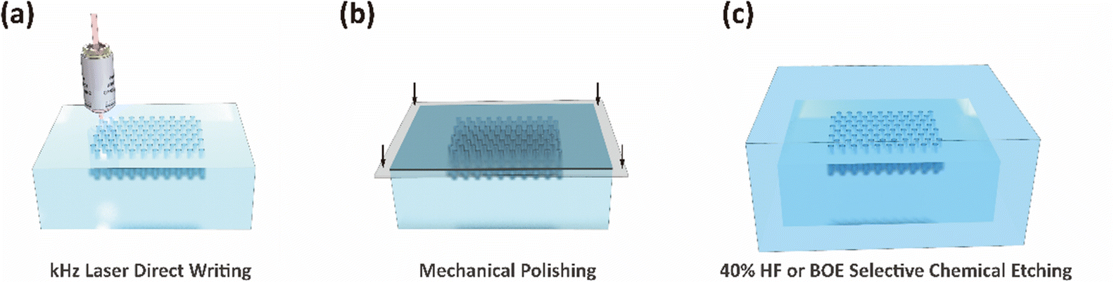 | ||
| Fig. 1 The fabrication process of LN nanostructure by using laser-induced selective chemical etching. First, we use a 1 kHz laser to write vertical lines inside LN crystal (a). Then, we Polish the sample until the laser-modified area is exposed (b). Finally, the sample is immersed into 40% HF or 6:1 BOE for chemical etching (c). | ||
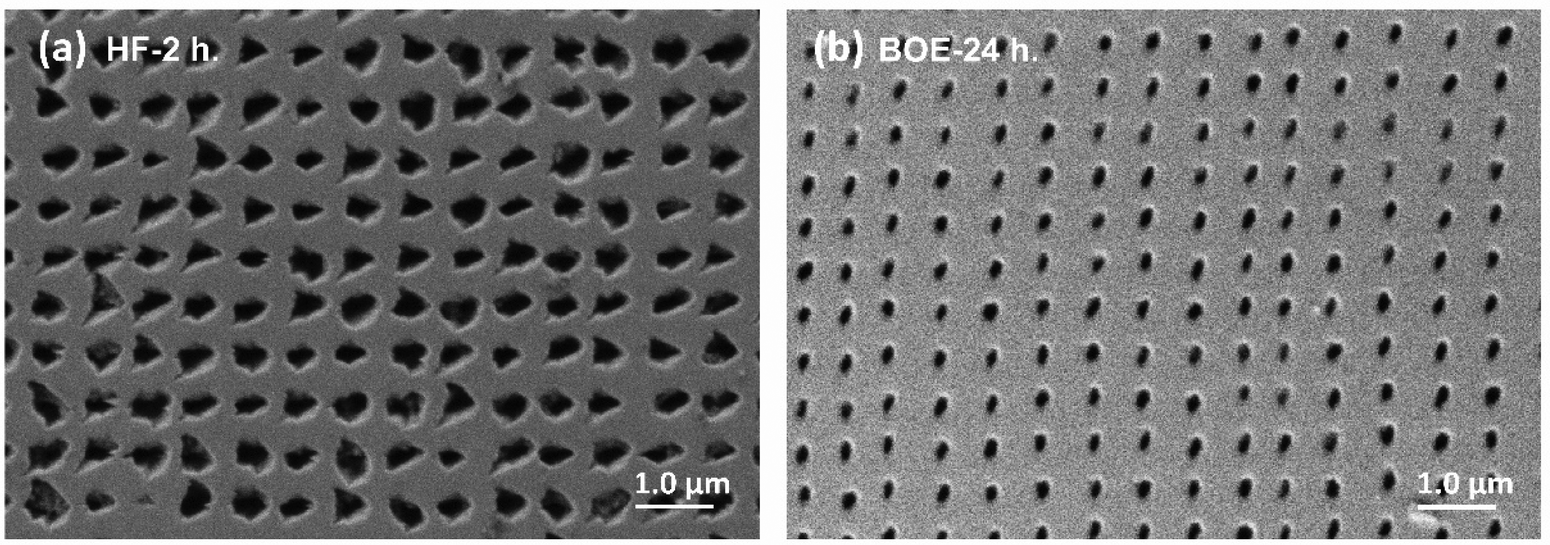 | ||
| Fig. 2 Comparison of the sample surface by using 40% HF (a) and BOE (b) in chemical etching. The pulse energy in prior laser writing is 11 nJ. The etching time is 2 hours and 24 hours for 40% HF and BOE, respectively. | ||
Next, we measure the etching rate. We use the focused femtosecond laser spot to write a series of lines along the depth direction. For each laser pulse energy, we write 10 lines with a length of 10 μm. The interval is set to be a few microns. After the polishing process, the sample is put into BOE for chemical etching. The sample is examined every 30 minutes by using an optical microscopy (Zeiss Axio Imager. Z2 under transmitted light illumination, Fig. 3(a)). The total etching time is 5 hours. The etching depth can be obtained by measuring the average length of the etched lines in Fig. 3(a). Under our experimental conditions, the laser-induced selectivity in chemical etching becomes clearly evident when the pulse energy is above a threshold value of 10 nJ. In Fig. 3, we compare the results using laser pulse energies of 10 nJ, 11 nJ and 12 nJ. Fig. 3(a) shows the microscopic images of these lines after different etching time. When setting the laser pulse energy at 10 nJ, one can hardly observe the lines being etched in a few hours. If using a higher laser pulse energy, one can see a clear increase in the length of the etched lines. However, when the etching time is beyond 3.5 hours, the line length does not further increase in our experiment. The etching process stops at a critical depth of 6.9 μm and 6.0 μm, corresponding to an incident pulse energy of 12 nJ and 11 nJ, respectively. The final length of the etched line is smaller than the laser writing distance of 10 μm. This can be explained by the fact that the refractive index mismatch between air and LN crystal results in a distorted laser spot inside the crystal.12,32,33 As increasing the fabrication depth, the distortion becomes severe so the laser energy density gradually decreases. At the critical depth, the energy density becomes too low to introduce enough selectivity in chemical etching. Fig. 3(b) shows the exponential dependence of the etching depth on the etching time. The initial etching rate is fast because the sample surface is fully immersed into the etchant. Then, the etching process gradually slows down until being completely stopped at the critical depth. For laser pulse energies of 12 nJ and 11 nJ, the average etching rates reach 2.0 μm h−1 and 1.7 μm h−1, respectively. In comparison to the reported etching rate of 3 nm h−1 for the original LN crystal by using HF–HNO3 etchant (3:2 volume ratio of 40% HF and 100% HNO3),19,22 the etching rate of BOE in the laser-modified area is enhanced by a factor of ∼660, which provides a useful way to fabricate LN nanostructure with a large aspect ratio.
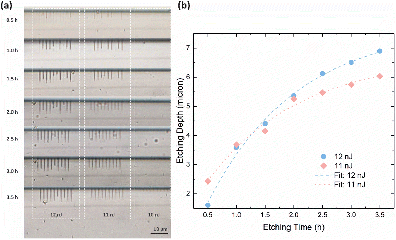 | ||
| Fig. 3 (a) The microscopic images of the etched lines after different etching time. The pulse energy in laser writing ranges from 10 nJ to 12 nJ. (b) The dependence of the etching depth on the etching time. The measured data well fit with an exponential function y = y0 + A1e−r·t. Here, y is the etching depth and t is the etching time. The fitting parameters of y0, A1 and r are decided by the final etching depth, the etching rate, and the decay of the etching rate. | ||
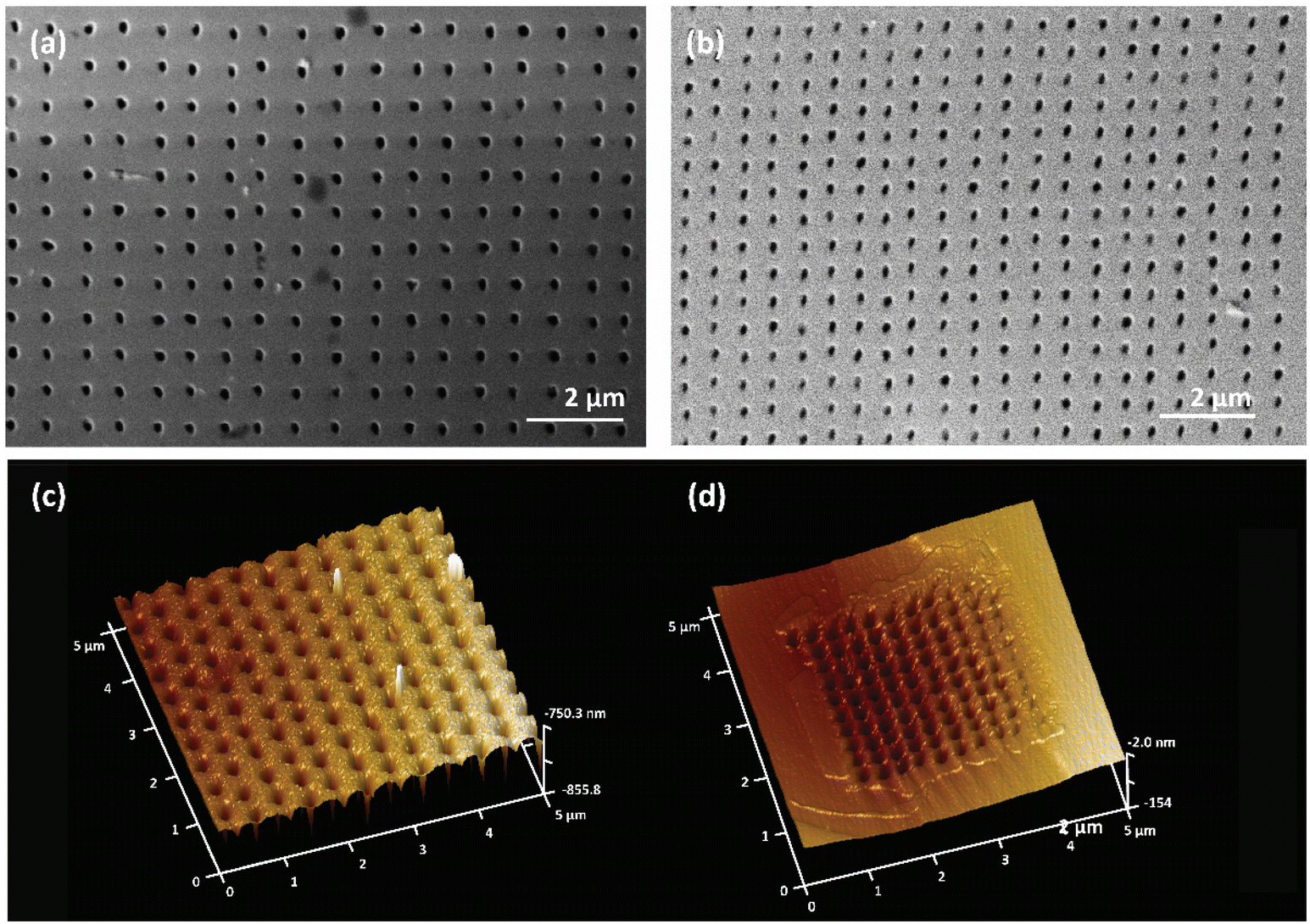
We use an atomic force microscope (AFM, Bruker icon, working at peak-force tapping mode) to characterize the in-plane structural dimension. Here, we employ a ScanAsyst-Air tip at a 0.5 Hz scan rate. Fig. 4 shows the AFM images by using different pulse energies. Here, we choose the samples after a 2-hour etching for comparison. One can observe uniform nanohole arrays. Each hole presents a nearly circular shape. For laser pulse energy of 11 nJ, the average widths along z and y directions are measured to be 118 nm and 98 nm, respectively (Fig. 4(a)). When increasing the pulse energy to 12 nJ, the average widths are increased to 216 nm and 196 nm along z and y directions, respectively (Fig. 4(b)). Here, the hole geometry is mainly decided by the profile of the focused laser spot. For pulse energies of 11 nJ and 12 nJ, the average etching depths after 2 hours are measured to be 5.05 μm and 5.30 μm, which correspond to aspect ratios above 40:1 and 20:1, respectively. In principle, one can tune the nanohole size by precisely controlling the pulse energy.
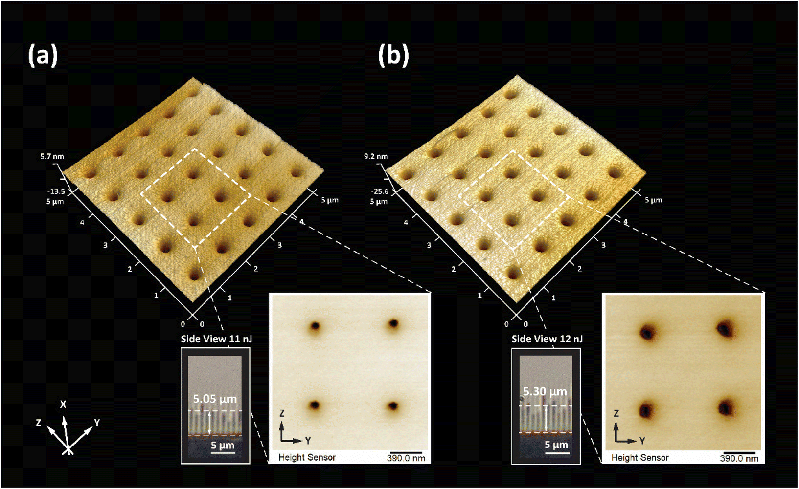 | ||
| Fig. 4 The AFM images of the sample surfaces by using pulse energies of 11 nJ (a) and 12 nJ (b). The etching time is 2 hours. The insets are the optical images of the side view of the structure. The average etching depths are 5.05 μm and 5.30 μm, respectively. | ||
In addition, we use this technique to fabricate LN nanohole arrays with periods down to submicron. Fig. 5(a) and (b) show the SEM images of the hole arrays with their periods being 800 nm and 600 nm, respectively. The pulse energy is 12 nJ and 11 nJ, respectively, and the BOE etching time is 24 hours. One can clearly see the uniform hole arrays. To further reduce the array period, one should carefully combine the parameters of laser writing and chemical etching. In the experiment, we use a laser pulse energy of 12 nJ and an etching time of 5 hours to realize a 500 nm-period triangular array (Fig. 5(c)) and a 300 nm-period square array (Fig. 5(d)). Due to the limitation in the repositioning accuracy of our translation stage (200 nm), it is difficult to further reduce the period under our current experimental setup.
 | ||
| Fig. 5 (a) and (b) show the SEM images of the nanohole arrays with periods of 800 nm and 600 nm, respectively. (c) and (d) are the AFM images of the nanohole arrays with periods of 500 nm and 300 nm, respectively. | ||
Conclusion
We have developed a femtosecond-laser-assisted nanolithography technique for LN crystal. By optimizing the parameters of laser writing and the subsequent chemical etching, the etching rate in x-cut LN crystal is enhanced to 2 μm h−1, which is significantly improved in comparison to previous reports.19,22 The interaction between high-energy laser pulses and LN results in the change in material properties such as local amorphization,15,16,34 which plays a crucial role in the improvement of the etching rate. Considering the effect of multiphoton absorption,1,2,13,35 the laser-induced local modification can be well confined within the focused spot. In addition, 1 kHz laser repetition frequency effectively reduces the local heat accumulation,1 leading to a high fabrication accuracy. Importantly, the use of BOE solution is critical to control the chemical interaction between the etchant and LN crystal. As a result, the etched structure is mainly decided by laser writing, which helps maintain a uniform LN nanostructure. Such unique advantages could be utilized to remove the existing issues in traditional etching techniques such as the irregular shape and unwanted scattering loss. In the experiment, we have achieved a nearly-circular nanohole with a size of ∼100 nm and an aspect ratio above 40:1. Our work provides a useful way for maskless fabrication of LN nanostructures. Besides the extreme photonic applications that require high-aspect-ratio 2D nanostructures, one can further upgrade this technique to realize 3D nanostructuring of LN crystals, which may open up the potential for 3D integrated LN devices.
Author contributions
YZ supervised the project. TW, XC, XL, JM, SY, XH, KQ, WF, ML, and XX performed the experiments under the guidance of XML, XJ, and YZ. TW designed the experiment and analyzed the data. TW and YZ wrote the manuscript with contributions from all co-authors.Conflicts of interest
There are no conflicts to declare.Acknowledgements
This work was supported by the National Key R&D Program of China (2022YFA1205100), the National Natural Science Foundation of China (NSFC) (91950206 and 92163216), the China Postdoctoral Science Foundation (2023M731587 and 2023T160303), the Yuxiu Young Scholars Program of Nanjing University, Postgraduate Research & Practice Innovation Program of Jiangsu Province (KYCX23_0094) and Fundamental Research Funds for the Central Universities (021314380226).References
- R. R. Gattass and E. Mazur, Nat. Photonics, 2008, 2, 219–225 CrossRef CAS.
- A. Rodenas, M. Gu, G. Corrielli, P. Paie, S. John, A. K. Kar and R. Osellame, Nat. Photonics, 2019, 13, 105–109 CrossRef CAS.
- D. Wei, C. Wang, X. Xu, H. Wang, Y. Hu, P. Chen, J. Li, Y. Zhu, C. Xin, X. Hu, Y. Zhang, D. Wu, J. Chu, S. Zhu and M. Xiao, Nat. Commun., 2019, 10, 4193 CrossRef PubMed.
- S. Liu, K. Switkowski, C. Xu, J. Tian, B. Wang, P. Lu, W. Krolikowski and Y. Sheng, Nat. Commun., 2019, 10, 3208 CrossRef PubMed.
- D. Z. Wei, C. W. Wang, H. J. Wang, X. P. Hu, D. Wei, X. Y. Fang, Y. Zhang, D. Wu, Y. L. Hue, J. W. Lie, S. N. Zhu and M. Xiao, Nat. Photonics, 2018, 12, 596–600 CrossRef CAS.
- T. X. Xu, K. Switkowski, X. Chen, S. Liu, K. Koynov, H. H. Yu, H. J. Zhang, J. Y. Wang, Y. Sheng and W. Krolikowski, Nat. Photonics, 2018, 12, 591–595 CrossRef CAS.
- M. Bazzan and C. Sada, Appl. Phys. Rev., 2015, 2, 040603 Search PubMed.
- J. Imbrock, L. Wesemann, S. Kroesen, M. Ayoub and C. Denz, Optica, 2020, 7, 28–34 CrossRef.
- L. Li, C. Romero, J. R. Vazquez de Aldana, L. Wang, Y. Tan and F. Chen, Opt. Express, 2019, 27, 36875–36885 CrossRef CAS PubMed.
- R. Wu, M. Wang, J. Xu, J. Qi, W. Chu, Z. Fang, J. Zhang, J. Zhou, L. Qiao, Z. Chai, J. Lin and Y. Cheng, Nanomaterials, 2018, 8, 910 CrossRef PubMed.
- F. He, H. Xu, Y. Cheng, J. Ni, H. Xiong, Z. Xu, K. Sugioka and K. Midorikawa, Opt. Lett., 2010, 35, 1106–1108 CrossRef PubMed.
- Y. Bellouard, A. Said, M. Dugan and P. Bado, Opt. Express, 2004, 12, 2120–2129 CrossRef CAS PubMed.
- R. Osellame, H. J. W. M. Hoekstra, G. Cerullo and M. Pollnau, Laser Photonics Rev., 2011, 5, 442–463 CrossRef CAS.
- F. He, Y. Cheng, Z. Xu, Y. Liao, J. Xu, H. Sun, C. Wang, Z. Zhou, K. Sugioka, K. Midorikawa, Y. Xu and X. Chen, Opt. Lett., 2010, 35, 282–284 CrossRef CAS PubMed.
- S. Juodkazis, K. Nishimura, H. Misawa, T. Ebisui, R. Waki, S. Matsuo and T. Okada, Adv. Mater., 2006, 18, 1361–1364 CrossRef CAS.
- E. G. Gamaly, S. Juodkazis, K. Nishimura, H. Misawa, B. Luther-Davies, L. Hallo, P. Nicolai and V. T. Tikhonchuk, Phys. Rev. B: Condens. Matter Mater. Phys., 2006, 73, 214101 CrossRef.
- C. Y. J. Ying, A. C. Muir, C. E. Valdivia, H. Steigerwald, C. L. Sones, R. W. Eason, E. Soergel and S. Mailis, Laser Photonics Rev., 2012, 6, 526–548 CrossRef CAS.
- A. B. Randles, M. Esashi and S. Tanaka, IEEE Trans. Ultrason. Ferroelect. Freq. Control, 2010, 57, 2372–2380 Search PubMed.
- H. Hu, R. Ricken, W. Sohler and R. B. Wehrspohn, IEEE Photonics Technol. Lett., 2007, 19, 417–419 CAS.
- I. E. Barry, G. W. Ross, P. G. R. Smith, R. W. Eason and G. Cook, Mater. Lett., 1998, 37, 246–254 CrossRef CAS.
- S. Grilli, P. Ferraro, P. De Natale, B. Tiribilli and M. Vassalli, Appl. Phys. Lett., 2005, 87, 233106 CrossRef.
- T. Wang, X. Xu, L. Yang, S. Yan, X. Hu, X. Hu, X. Lu, M. Xiao and Y. Zhang, Nanophotonics, 2022, 11, 829–834 CrossRef CAS.
- V. Bermúdez, F. Caccavale, C. Sada, F. Segato and E. Diéguez, J. Cryst. Growth, 1998, 191, 589–593 CrossRef.
- F. Laurell, J. Webjorn, G. Arvidsson and J. Holmberg, J. Lightwave Technol., 1992, 10, 1606–1609 CrossRef CAS.
- Y. Li, T. Lan, D. Yang, M. Xiang, J. Dai, C. Li and Z. Wang, Mater. Res. Express, 2020, 7, 056202 CrossRef CAS.
- X. Xu, T. Wang, P. Chen, C. Zhou, J. Ma, D. Wei, H. Wang, B. Niu, X. Fang, D. Wu, S. Zhu, M. Gu, M. Xiao and Y. Zhang, Nature, 2022, 609, 496–501 CrossRef CAS PubMed.
- H. Steigerwald, Y. J. Ying, R. W. Eason, K. Buse, S. Mailis and E. Soergel, Appl. Phys. Lett., 2011, 98, 062902 CrossRef.
- S. Mailis, C. Sones and R. Eason, in Ferroelectric Crystals for Photonic Applications: Including Nanoscale Fabrication and Characterization Techniques, Springer, 2014, pp. 3–19 Search PubMed.
- A. A. Anikiev, N. V. Sidorov, M. N. Palatnikov, M. F. Umarov and E. N. Anikieva, Opt. Mater., 2021, 111, 110729 CrossRef CAS.
- M. D. Fontana and P. Bourson, Appl. Phys. Rev., 2015, 2, 040602 Search PubMed.
- S. Sanna and W. G. Schmidt, J. Phys.: Condens.Matter, 2017, 29, 413001 CrossRef PubMed.
- R. D. Simmonds, P. S. Salter, A. Jesacher and M. J. Booth, Opt. Express, 2011, 19, 24122–24128 CrossRef CAS PubMed.
- A. Jesacher and M. J. Booth, Opt. Express, 2010, 18, 21090–21099 CrossRef CAS PubMed.
- T. Y. Choi and C. P. Grigoropoulos, J. Appl. Phys., 2002, 92, 4918–4925 CrossRef CAS.
- J. Krüger and W. Kautek, Appl. Surf. Sci., 1996, 96–98, 430–438 CrossRef.
| This journal is © The Royal Society of Chemistry 2023 |