
 Open Access Article
 This Open Access Article is licensed under a Creative Commons Attribution-Non Commercial 3.0 Unported Licence
The emergence of amorphous materials approaching the single-layer limit
Zude
Shi†
a,
Haowei
Ge†
a and
Yongmin
He
 *ab
*ab
aState Key Laboratory of Chemo and Biosensing, College of Chemistry and Chemical Engineering, Hunan University, Changsha 410082, China. E-mail: ymhe@hnu.edu.cn
bGreater Bay Area Institute for Innovation, Hunan University, Guangzhou 511300, China
First published on 3rd September 2025
Abstract
Amorphous materials with thickness thinned down to the single-layer limit have attracted increasing interest due to their well-defined disorder and emerging unique properties, such as disorder-dominated electronic states, high-density unsaturated coordination, enhanced quantum confinement, etc. These features could enable innovative applications in electronics, photoelectronics, catalysis, and beyond. In this perspective, we provide an overview of recent advances in two-dimensional (2D) amorphous materials approaching the single-layer limit. We first introduce newly-developed key structural descriptors for these systems, including local bonding, topological disorder, and chemical composition. Next, we highlight fabrication breakthroughs across diverse material classes, such as amorphous carbon, oxides/hydroxides, metals, transition metal dichalcogenides (TMDCs), and metal/covalent–organic frameworks (MOFs/COFs). The resulting properties, spanning electrical/electrocatalytic properties, mechanical toughness, photoelectric response, and topological electronic states, are subsequently discussed. Finally, we outline current challenges and future opportunities in this rapidly evolving field.
1. Introduction
Unlike their crystalline counterparts, amorphous materials typically exhibit unique properties, such as isotropic atomic environments, abundant surface dangling bonds, highly-unsaturated coordination, etc.1–3 These unique features have led to various promising applications in electronic devices, energy storage, photo-electrocatalysis, and other fields.3–6 As early as 1841, Liebig et al. reported that sulfur in the amorphous state became soft and transparent, presenting distinctive properties compared with its crystalline form.7 In 1934, Kramer et al. pioneered the systematic preparation of amorphous metals using a vapor deposition method, through which condensing high-temperature metal vapors on ultralow-temperature substrates facilitates the preservation of disordered structures.8 In 1960, Duwez et al. reported the successful synthesis of an amorphous Au–Si alloy through rapid quenching from its molten state.9 Subsequently, Marchal et al. discovered its superconducting properties, which are related to the presence of a fixed stoichiometric amorphous alloy close to Au3Si.10At the turn of the 21st century, Inoue et al. found a series of new multicomponent alloyed systems with significantly lower critical cooling rates, and proposed three experimental guidelines for their preparation. Among these systems, Zr-based bulk amorphous alloys exhibit high mechanical strength, remarkable fracture toughness, and good corrosion resistance.11 In 2011, Chen et al. reported the direct observation of local atomic order in three-dimensional metallic glass using an electron nanoprobe combined with ab initio molecular dynamics simulation; the findings provided compelling evidence of local atomic order in disordered metallic glass.12 These continuing advances demonstrate that the field of amorphous materials is both ancient and fascinating, leaving a vast scope to explore the unique behavior of disordered material systems.
Recently, emerging 2D materials with a single-layer thickness, exemplified by graphene,13 ultra-thin oxides,14–16 and TMDCs,17 have attracted tremendous research interest across various fields. These 2D systems typically exhibit distinct thickness-dependent quantum confinement effects, ultra-strong in-plane covalent bonds, unique electronic states induced by local structural fluctuations, etc.4,6,18–23 Remarkably, they often deliver unique and remarkable properties that are distinct from those of their bulk counterparts, as illustrated in Fig. 1a. These achievements in 2D materials raise an interesting and open question: what will happen in amorphous materials when they are thinned down to the single-layer limit (see Fig. 1b)?
 | ||
| Fig. 1 Thinning of bulk materials to the single-layer limit. (a) Thinning of bulk layered materials to obtain a stable crystalline single-layer, with a unit-cell thickness. (b) Thinning of bulk amorphous materials approaching the single-layer limit. In the atomically thin amorphous system, the intrinsically disordered structure will be well preserved (stochastic atomic packing, exemplified by Zachariasen's continuous random network (Z-CRN)). | ||
Inspired by this question, a series of atomically thin amorphous materials, such as carbon,24–26 oxides,27,28 and TMDCs,29,30 have been reported more recently. Many fascinating properties can emerge when their thickness approaches the single-layer limit. Taking the example of single-element amorphous materials, monolayer amorphous carbon (MAC) has been successfully synthesized through a low-temperature chemical vapor deposition (CVD) method. It demonstrates remarkable mechanical strength and tunable electrical conductivity, opening up new opportunities for applications in ultrathin flexible electronics.25,26 Moreover, dozens of amorphous noble metal nanosheets could be successfully prepared at the single-layer limit by annealing the mixture of metal acetylacetonate and alkali salts, some of which exhibit superior performances for the oxygen evolution reaction (OER) in acidic media.31 Beyond this, for two- or more-element amorphous materials, 1-nm-thick amorphous PtSex films can be fabricated through ultralow-temperature plasma etching, exhibiting high efficiency in the hydrogen evolution reaction (HER).29 Additionally, ultra-thin HfO2 nanosheets, which can be easily synthesized through oxidation of liquid metal at room temperature, exhibit excellent dielectric properties.27,28
The achievements above encourage us to provide a timely review, which would arouse wide attention for further development in this amorphous field. It is noteworthy that some excellent reviews have been presented before;1,3,18–20,32 unfortunately, less attention has been paid to this newly-emerged 2D amorphous system, especially for the one approaching the single-layer limit. In this review, we will first discuss recently-developed key structural descriptors for single-layer amorphous materials, including local bonding, topological disorder, and chemical composition. Then, we will introduce representative types of well-synthesized 2D amorphous materials, including carbon, oxides/hydroxides, TMDCs, metals, MOFs/COFs, and other potential amorphous materials, along with their detailed synthesis methods. Thereafter, how these disordered atomic arrangements correlate with the resulting electronic, electrocatalytic, mechanical, optoelectronic, and topological properties will be discussed. Finally, we will provide our perspectives on key challenges involving theoretical optimization, fabrication mechanisms, and stability engineering, as well as an exploration focusing on the materials library and its implications.
2. Key structural parameters
In amorphous bulk materials, it is challenging to determine whether their disordered structure follows Zachariasen's continuous random network (CRN) model or the crystallites embedded in CRN (C-CRN) framework, proposed by Lebedev in 1921.18,26 Fortunately, this challenge could be overcome by 2D amorphous materials because their atomic thickness enables atomic-scale imaging by scanning transmission electron microscopy (STEM), offering unique advantages for resolving those disordered structures. As a result, the local bonding, topological disorder, and chemical composition could be clearly identified in 2D amorphous systems. This section discusses key structural parameters (Fig. 2) and their corresponding characterization methods. | ||
| Fig. 2 Key structural parameters of 2D amorphous materials. The key structural parameters of amorphous materials can be categorized into three types: local bonding, topological disorder, and chemical composition. RDF: radial distribution function. DHU: disordered hyperuniformity. | ||
2.1. Local bonding
Local bonding in 2D amorphous materials is defined by deviations from crystalline symmetry and hybridization states, which can be described in detail by the radial distribution function (RDF) and bond angle/length distribution (the top of Fig. 2). Their parameters can be experimentally determined using X-ray absorption spectroscopy (XAS), Raman spectroscopy, STEM, etc.The RDF describes how atomic density varies as a function of distance from a reference particle. By analyzing specific peaks corresponding to interatomic distances, RDF reveals the degree of short/medium/long-range order (SRO/MRO/LRO) in a material. In MAC films, compared to the sharp peaks in the g(r) of graphene, all MAC samples exhibit broader peaks on the short-range scale, verifying their short-range orders.25 Moreover, their structures could be further tuned by the different synthesis temperatures, ranging from weak orders to the completely amorphous structure. On the other hand, bond angle and length distributions have also been used to refine the local bonding, which involves quantifying the equilibrium distances between nearest-neighbor atoms and the angular configurations formed by three consecutively bonded atoms. For example, in MAC, bond angles span 90°–150° compared to the rigid 120° in crystalline graphene. At the same time, bond-length variations (0.9–1.8 Å) reflect strained sp2 networks in MAC.26
These parameters, often verified by STEM imaging and molecular dynamics (MD) simulations, are able to quantify the degree of disorder at the atomic scale and identify hybridization states (sp2vs. sp3) as well.25,33
2.2. Topological disorder
Topological disorder is another crucial structural parameter in 2D amorphous systems, directly reflecting structural randomness and local atomic density fluctuations. It consists of two parameters: disordered hyperuniformity (DHU) and ring statistics, where the former involves quantifying density fluctuations across different length scales and the latter is determined by non-crystalline ring configurations (the middle of Fig. 2), that is, the fraction of pentagons, hexagons, heptagons, etc. These characteristics can be analyzed by STEM, selected area electron diffraction (SAED), and scanning tunneling microscopy (STM).A system with the DHU typically exhibits lower energy states than other disordered ones, which enables unique electronic and thermal transport properties.34 For example, in the single-layer amorphous silica, DHU could be identified through spectral-density analysis of HRTEM images, which originates from the continuous introduction of Stone–Wales (SW) defects during synthesis.35 Remarkably, such silica displays metallic behavior, a phenomenon attributed to the localization of high-energy states induced by topological defects.36
The ring statistics is the other important parameter because the structural disorder in amorphous materials strongly correlates with deviations from crystalline ring geometries. For instance, low-voltage STEM reveals distinct ring statistics between MAC samples synthesized at 300 °C and 400 °C.25 For the one synthesized at 300 °C, hexagonal carbon rings account for approximately 86% of the carbon ring structures. In these hexagonal rings, the majority (∼67%) were embedded within nanocrystallites, with the remainder as isolated hexagons (∼19%). In contrast, MAC synthesized at 400 °C exhibits a higher proportion of isolated hexagons (∼45%) and an abundance of 5/7/8-membered rings (∼28%), indicating a higher degree of structural disorder. Notably, the former (300 °C) possesses electrical conductivity nine orders of magnitude higher than that of the latter (400 °C).
2.3. Chemical composition
Compared to their crystalline counterparts with fixed stoichiometry, amorphous materials exhibit more flexibility in the chemical composition, one of the core parameters for material design and later performance control. Chemical composition mainly includes the species and proportions of chemical elements (the bottom of Fig. 2), which can be characterized by XAS, X-ray photoelectron spectroscopy (XPS), energy-dispersive X-ray spectroscopy (EDS), and electron energy-loss spectroscopy (EELS).As for the elemental species, it can effectively modulate the structural and electronic properties of amorphous materials. Recent studies have demonstrated that doping N single atoms into sp2 hybridized MAC enables uniform N distribution at a concentration of approximately 9 at%, as verified by EELS.24 XAS indicates that the doped N atoms exhibit a preferential graphitic-N configuration, with minor amounts of pyridinic and pyrrolic N species. This N-doped modification of MAC induces a transition from an insulating state to a p-type behavior.
On the other hand, in light of the proportions of chemical elements in amorphous materials, we took amorphous PtSex as another typical example.29 XPS and XAS reveal that a decrease in the Se/Pt atomic ratio from 2 to 1.3 induces a structural collapse of the crystalline lattice in PtSex films, ultimately leading to the formation of a monolayer amorphous structure. This stoichiometric modification triggers an electronic transition from p-type semiconducting behavior to a metallic state as well as a significantly enhanced HER catalytic activity.
3. Fabrication strategies
This section will discuss recently-reported 2D amorphous materials, including carbon, oxides/hydroxides, TMDCs, metals, 2D MOFs/COFs, etc., together with their fabrication strategies and mechanisms, morphological features, and structural parameters. Notably, given that the 2D amorphous materials are non-layered structures, the fabrication approaching the single-layer limit remains a significant challenge. Taking this into consideration, we classified current fabrication strategies into bottom-up and top-down strategies. The former focused on how to grow 2D amorphous layers, while the latter emphasized how to etch crystalline parent materials to realize crystalline-to-amorphous transformation. Lastly, other potential amorphous materials approaching the single-layer limit will be suggested.3.1. Amorphous carbon-based materials
Similar to the primary role of graphene in the 2D material field, MAC has also emerged as a classic disordered material for exploring the unique structure and properties of 2D amorphous systems.20 Recent significant advances in the synthesis and atomic-scale characterization of MAC position it at the forefront of amorphous materials.24–26 A series of fabrication methods, including CVD (bottom-up), space-confined solution synthesis (bottom-up), and e-beam or ion-based etching (top-down), will be introduced in the following sections.Inspired by the CVD growth of graphene layers on metal substrates, most MACs have been synthesized through vapor growth methods. Unlike graphene, the nucleation and growth of MACs require non-equilibrium kinetic conditions, and impressively, a low-temperature condition is necessary to suppress lattice relaxation and prevent crystallization. The first example is that Özyilmaz et al. utilized laser-assisted CVD (LCVD) to synthesize a centimeter-scale MAC film, as shown in Fig. 3a and b.26,37 The synthesized film shows randomly oriented crystallites embedded within CRN. Using STEM, they revealed that it presents broad distributions of bond length (0.9–1.8 Å) and bond angle (90°–150°), as well as a dominance of 5-, 6-, 7-, and 8-membered rings (Fig. 3c). Furthermore, the RDF analysis confirmed the loss of long-range periodic order in MAC, which was distinguished from graphene (Fig. 3d). Another interesting example is that Liu et al. synthesized the MAC film using low-temperature CVD combined with pyrolysis of a polycyclic heteroarene (Fig. 3e and f).25 They observed the temperature-dependent degree of amorphization in the synthesized MAC, with the one synthesized at 400 °C exhibiting the highest degree of amorphization in Fig. 3g.
 | ||
| Fig. 3 Synthesis and structure of amorphous carbon-based materials. (a) Schematic of monolayer amorphous carbon (MAC) growth via laser-assisted CVD (LCVD). Reproduced with permission.37 Copyright 2014, Laser Institute of America. (b and c) Photograph (b) and high-resolution transmission electron microscopy (HRTEM) image (c) of MAC. (d) Radial distribution function calculated by the atomic coordinates of graphene and MAC. Reproduced with permission.26 Copyright 2020, Springer Nature. (e) Schematic of MAC growth via CVD using the cyclic aromatic molecule as the precursor. (f) Optical microscopy image of MAC-400. (g) Denoised annular dark-field scanning TEM (ADF-STEM) image and representative nano-beam electron diffraction (NBED) pattern of MAC-400. Reproduced with permission.25 Copyright 2023 Springer Nature. (h) Schematic of nitrogen-doped MAC (NMAC) synthesized by confined polymerization using solid templates and an ion exchange strategy. (i) Atomic force microscopy (AFM) image and the corresponding height profile of the as-grown NMAC flake. (j and k) High-magnification ADF-STEM image and the corresponding EELS map of NMAC, with N atoms highlighted by red dashed circles. Reproduced with permission.24 Copyright 2024 Springer Nature. | ||
The spatial confinement strategy can effectively enhance the in-plane arrangement and assembly, facilitating the growth process of 2D amorphous materials. Most recently, Guo et al. employed layered double hydroxide (LDH) templates to orchestrate the radical polymerization of pyrrole monomers within sub-nanometer interlayer cavities, as shown in Fig. 3h.24 The resulting nitrogen-doped MAC (NMAC) nanosheet exhibited a single-layer thickness (Fig. 3i). Using Raman spectroscopy and XAS, they revealed the extended in-plane π-conjugation of NMAC. Systematic STEM characterizations confirmed that this material features unique topological motifs, dominated by distorted 5–6–7-membered ring configurations. Spatially averaged EELS also quantified the nitrogen content in the NAMC sample at approximately 9 at%, confirming successful nitrogen incorporation (Fig. 3j and k). Notably, the spatial confinement strategy induced a threefold reduction in the SW transformation activation energy, enabling the thermodynamic stabilization of the amorphous structure through space-confined solution synthesis. In addition, there are also other excellent examples of bottom-up strategies, such as solution-based approaches on non-catalytic substrates,38 substrate-lattice-mismatched growth, etc.39
The top-down etching strategy was also used to fabricate MAC by gradually damaging the lattice structure of the parent graphene. For example, Eom et al. investigated graphene's structural and electrical evolution under electron beam irradiation.40 Increasing irradiation doses generated more defects in graphene samples, which would evolve from nanocrystalline to amorphous. Similarly, Kotakoski et al.41 also investigated how disorders occur in monolayer graphene under low-energy argon ion irradiation and employed convolutional neural networks for STEM image analysis. The authors demonstrated that graphene is gradually amorphized through the formation of non-hexagonal carbon rings, in sharp contrast to stable h-BN, which preserves its crystalline structure. To further explore how the graphene changes into an amorphous state, Zhuang et al. discovered a topological transition in the 2D disordered network of MAC, which preserves DHU through the continuous introduction of SW defects.35 Moreover, their theoretical structural model, at a specific defect concentration (0.06), was successfully aligned with both the local topological order and the large-scale spatial correlations observed in experimental MAC films.
The unique characteristics of the above MAC hold great potential applications in mechanics, electronics, and energy storage. For example, its CRN guides crack propagation along tortuous paths under external stress, thereby enhancing the material's toughness. This crack-propagation behavior makes MAC ideal for protective coatings in harsh environments.26,42,43 In electronics, the degree-of-disorder-tuned conductivity of MAC enables the realization of conductive patterns that spatially control conductivity within a single layer, which is highly desirable for flexible electronic devices.44 Furthermore, based on its high density of atomic-scale defects (specifically 8-carbon rings), it exhibits selective permeability, allowing efficient transport of protons (about three orders of magnitude higher than that of defect-free graphene) and Li ions while completely blocking gases and liquids.45 This molecular/ionic selectivity makes it highly suitable for hydrogen technologies (e.g., proton-exchange membranes) and Li-ion batteries (e.g., advanced separators or protective barriers).
3.2. Amorphous oxide/hydroxide layers
With respect to the bottom-up synthesis strategy of 2D amorphous oxides/hydroxides, Daeneke et al. developed a gas injection method to synthesize amorphous oxide nanosheets (HfO2, Al2O3, and Gd2O3) approaching single-layer thickness by oxidizing liquid metals through an air injection method,28 as shown in Fig. 4a and b. TEM and SAED characterizations revealed the amorphous structure of the HfO2 nanosheets (Fig. 4c), likely attributed to the short residence time of bubbles in the liquid metal and rapid oxidation kinetics, which limited the time available for crystallization. This finding offers a novel strategy for synthesizing oxides that approach the single-layer limit. | ||
| Fig. 4 Synthesis and structure of amorphous oxides/hydroxides. (a) Schematic of air oxidation of liquid metal for synthesizing single-layer-limit oxides (left) and optical image of the nanosheets drop-cast onto the SiO2/Si substrate (right). (b) AFM image and the corresponding height profile of single-layer-limit HfO2. (c) TEM image, selected-area electron diffraction (SAED) (top inset) and HRTEM image (bottom inset) of single-layer-limit HfO2. Reproduced with permission.28 Copyright 2017 the American Association for the Advancement of Science. (d) Schematic of single-layer-limit MoO3 growth via UV-ozone-driven oxidation. (e) Comparison of optical microscope images of single-layer MoS2 grown on 2-inch sapphire substrates before (left) and after oxidation (right). (f) ADF-STEM image of single-layer-limit MoO3. Inset: the corresponding high-magnification ADF-STEM image. Reproduced with permission.46 Copyright 2022 American Chemical Society. (g) Schematic of the electrochemical conversion strategy for synthesizing single-layer-limit amorphous Ni(OH)2. (h) AFM image and the corresponding height profiles of the as-converted single-layer-limit amorphous Ni(OH)2 nanosheets. (i) High-angle ADF-STEM (HAADF-STEM) image and the corresponding fast Fourier transform (FFT) pattern of the as-converted single-layer-limit amorphous Ni(OH)2 nanosheets. Reproduced with permission.47 Copyright 2022 American Chemical Society. (j) Schematic of solid-state surfactant-templated synthesis of single-layer-limit amorphous oxide/oxyhydroxide nanosheets. (k and l) AFM image, the corresponding height profiles (k), TEM image and SAED pattern (l) of the single-layer-limit amorphous gallium oxide/oxyhydroxide nanosheets. Reproduced with permission.48 Copyright 2024 Springer Nature. | ||
On the amorphous-hydroxide side, Osada et al. developed a solid-state surfactant templating strategy to synthesize amorphous 2D oxide/oxyhydroxide nanosheets with controlled thicknesses (0.7–5.5 nm) and diverse compositions, including Al3+, Sc3+, Mn3+, Fe3+, Co3+, Ga3+, In3+, and Rh3+ (Fig. 4j–l).48 In this approach, metal ions are arranged within the interlayer spaces of solid-state surfactant crystals. Subsequent hydrolysis of these ions induces limited condensation reactions, resulting in the formation of isolated clusters within the surfactant framework. To achieve 2D layers, the authors immersed the surfactant crystals in formamide, which promotes the self-assembly of clusters by templating the surfactant crystal morphologies.
In the top-down fabrication of amorphous oxides, Akinwande et al. demonstrated an ultraviolet-ozone (UV-O3) oxidation to convert wafer-scale monolayer MoS2 into an amorphous MoO3 layer (∼0.7 nm) (Fig. 4d).46 Optical microscopy revealed a stark contrast between the pristine MoS2 and the transparent oxidized film (Fig. 4e). Atomic-resolution STEM (Fig. 4f) confirmed the absence of long-range order, a characteristic of amorphous structures. On the other hand, for amorphous hydroxides, Guo et al. synthesized amorphous Ni(OH)2 nanosheets through an in situ electrochemical conversion strategy (Fig. 4g).47 The atomic force microscopy (AFM) characterization revealed the single-layer limit of the resulting material, with a uniform thickness of approximately 0.8 nm (Fig. 4h). The HAADF-STEM image and the corresponding fast Fourier transform (FFT) pattern show the disordered atomic arrangement of Ni atoms (Fig. 4i).
In both aforementioned synthesis strategies, the amorphous oxides and hydroxides obtained at the single-layer limit offer distinct advantages over their crystalline counterparts in various applications. In electrocatalysis, single-layer amorphous hydroxide nanosheets, such as Ni(OH)2 and Co(OH)2, have demonstrated enhanced energy storage and OER activity due to their high density of defective sites and improved charge/ion transfer capabilities.47,49 In electronic and optoelectronic devices, single-layer amorphous oxides with atomic-scale uniformity and high dielectric constants, such as amorphous HfO2, can be used for gate dielectrics in field-effect transistors, benefiting from their low leakage currents and conformal coverage.28 Moreover, their large optical bandgaps and transparency enable their integration into flexible and transparent electronic devices.50,51
3.3. Amorphous metal layers
Top-down approaches offer the potential for controllable fabrication of amorphous metal films with tailored coordinations; however, thinning them down to a single layer remains challenging.52,53 Alternatively, bottom-up approaches, which benefit from operational flexibility and scalable production, exhibit significant advantages in precisely controlling key parameters, such as monolayer thickness, amorphous structural stability, and atomic coordination environment.31 To date, a large number of bottom-up approaches have been developed for synthesizing amorphous metals approaching the monolayer limit, such as alkali metal salt-assisted growth,31 template-based methods,54 hydrothermal/solvothermal methods,55 and surfactant assembly approaches,56 among others.As a pioneering work, Li et al. developed an alkali salt-assisted annealing method to fabricate amorphous metal nanosheets with tunable thickness and controllable composition (Fig. 5a).31 This method can achieve micrometer-scale amorphous nanosheets, approaching the single-layer thickness, as illustrated in Fig. 5b. These nanosheets exhibit amorphous features, with disordered atomic arrangement, loosely bonded structures, and high-density defect sites. Further characterization via HAADF-STEM and SAED techniques reveals a disordered atomic arrangement of Ir metal atoms (Fig. 5c). In a subsequent study, Liu et al. proposed a DNA-templated rapid synthesis protocol at room temperature, allowing for the controlled preparation of amorphous copper nanosheets with large lateral dimensions (Fig. 5d).54 Small-angle X-ray diffraction reveals nanoscale periodicity coexisting with atomic-level disorder in the nanosheets (Fig. 5e). Notably, the sample still exhibited typical amorphous halos through TEM/SAED analysis, even at areas exceeding 150 μm2. On the other hand, Zhang and colleagues reported a thiol ligand-exchange-induced amorphization strategy, synthesizing stable amorphous Pd NSs at ambient temperature (Fig. 5g).55 Using HRTEM, the authors could capture the phase evolution from crystalline to crystalline/amorphous composite and finally to fully amorphous states (Fig. 5i), suggesting that this method is extendable to fabricate crystalline-amorphous heterojunctions. Later, using a similar approach, Zhang and co-workers demonstrated a surfactant-free wet-chemical approach to synthesize amorphous/crystalline rhodium nanosheets (a/c-Rh NSs) approaching the single-layer limit.56 The complementary characterizations confirmed that the heterostructure exhibits atomic-level structural disorder, characterized by abundant phase boundaries and low coordination numbers.
 | ||
| Fig. 5 Synthesis and structure of amorphous metals. (a) General synthesis schematic for amorphous noble metal nanosheets (NSs), where M. T. denotes the melting temperature of metal acetylacetonate precursors. (b) TEM image of amorphous iridium NSs reveals their morphology approaching the single-layer limit. (c) Aberration-corrected HAADF-STEM image of amorphous Ir NSs. Inset: characteristic diffuse-ring SAED patterns indicative of long-range disorder. Reproduced with permission.31 Copyright 2019 Springer Nature. (d) DNA nanosheet (DNS)-templated synthesis strategy for amorphous copper nanosheets (DNS/CuNSs). (e) Small-angle X-ray diffraction (XRD) plots of DNS/CuNSs, DNS, and dsDNA. (f) TEM micrograph of 2D amorphous DNS/CuNSs approaching the single-layer limit. Inset: SAED patterns. Reproduced with permission.54 Copyright 2023 American Chemical Society. (g) Chemical bath deposition protocol for synthesizing amorphous Pd NSs. Reproduced with permission. Copyright 2018 Springer International Publishing AG. (h) TEM image of bismuth thiol I-capped amorphous Pd NSs reacted for 24 h (Pd NSs-Bis-24 h). Insets: molecular structure of the bismuthiol I ligand (top) and corresponding SAED pattern (bottom). (i) HRTEM image of Pd nano-island-Bis-24 h, demonstrating the absence of lattice fringes. Reproduced with permission.55 Copyright 2020 John Wiley & Sons. | ||
Towards applications of amorphous metal layers, amorphous Ir nanosheets exhibit 2.5 times higher acidic oxygen evolution activity than crystalline Ir in catalysis, attributed to their abundant coordination defects. Similarly, amorphous Pd nanosheets achieve an ultralow HER Tafel slope of merely 30 mV dec−1 due to elongated Pd–Pd bonds that optimize hydrogen adsorption energy.55 In optoelectronics, DNA-templated amorphous Cu nanosheets show 62-fold enhanced fluorescence intensity with superior stability, where elevated conduction/valence bands promote carrier separation.54 For chemical synthesis, amorphous/crystalline heterophase RhCu nanosheets catalyze indole formation with 100% conversion and >99.9% selectivity, where phase interfaces accelerate nitro reduction and Cu alloying suppresses side reactions.56
3.4. Amorphous transition metal dichalcogenides
Significant efforts have also been devoted to top-down fabrication strategies of amorphous TMDCs at the single-layer limit, such as supercritical strain engineering,57 low-temperature ion etching,29 and low-energy glancing-angle ion beam irradiation.58 For example, Xu's group recently demonstrated a supercritical carbon dioxide-assisted approach with precise pressure regulation (20 MPa) and temperature gradients (40–80 °C) to achieve controlled amorphization of VS2 nanosheets in a water/NMP solvent system (Fig. 6a). This approach enables establishing a new paradigm for precision engineering of functional amorphous materials.57 Microscopic characterization revealed a high specific surface area and the absence of crystalline lattice fringes (Fig. 6b). STEM elemental mapping (V/S) combined with SAED diffuse rings (Fig. 6c) collectively confirmed the amorphous atomic structures of these VS2 nanostructures. | ||
| Fig. 6 Synthesis and structure of amorphous 2D TMDCs. (a) Synthesis strategy for 2D amorphous VS2 nanosheets via supercritical CO2-assisted fabrication. (b) HRTEM image confirming the amorphous phase and morphology of VS2 nanosheets, approaching the single-layer limit. (c) STEM image with elemental mapping (V/S) and corresponding SAED patterns, demonstrating long-range structural disorder. Reproduced with permission.57 Copyright 2020 John Wiley & Sons. (d) Wafer-scale production of amorphous PtSex films: amorphization process using deep reactive-ion etching (DRIE) under low-energy Ar plasma at −30 °C. (e) Cross-sectional HAADF-STEM image of the amorphous PtSex layer. (f) Atomic-resolution HAADF-STEM image of the amorphous PtSex film over large areas. Inset: FFT pattern showing diffuse scattering characteristics. Reproduced with permission.29 Copyright 2022, Springer Nature. (g) Strategy for synthesizing amorphous MoS2 using a low-energy grazing-incidence ion irradiation technique: Xe+ ion (500 eV) bombardment on MoS2/Gr/Ir (111) at polar (θ = 75°) and azimuthal (φ = 27.5°) angles. (h) Post-irradiation surface analysis: scanning tunneling microscopy (STM) topography (left), height profile and LEED pattern (right) of MoS2 after 1.5 × 10¹⁴ ions/cm2 Xe+ irradiation at 500 eV. The arrow indicates ion beam projection. Reproduced with permission.58 Copyright 2024 IOP publishing. | ||
More recently, He et al. developed a low-temperature plasma etching strategy to fabricate amorphous PtSex single-layer-limit (∼1 nm) catalysts (Fig. 6d), exhibiting platinum-like catalytic activity with exceptional atomic utilization efficiency.29 Cross-sectional HAADF-STEM identified surface amorphization (demarcated by white dashed lines), with intensity profile inhomogeneity (Fig. 6e) and atomic spacing fluctuations together suggesting significant in-plane Pt displacements. Atomic-resolution HAADF imaging revealed random Pt distribution (Fig. 6f), complemented by broad FFT halos (the inset of Fig. 6f), providing sufficient evidence for large-area complete amorphization. Most recently, Valerius et al. implemented a low-energy grazing-incidence ion irradiation technique. The authors utilized 500 eV Xe+ ions at a 75° incidence to selectively sputter top-layer sulfur atoms, thereby amorphizing single-layer MoS2 on graphene/Ir(111) substrates (Fig. 6g).58 STM analysis showed a tenfold increase in surface roughness (0.01 → 0.1 nm), and the disappearance of the LEED pattern verified the destruction of long-range order.
On the other hand, the bottom-up synthesis of amorphous TMDCs approaching the single-layer limit mainly involves atomic layer deposition (ALD),59 physical vapor deposition (PVD),60 CVD,61 and a melt-and-quench process.62 For instance, Kim et al.59 successfully prepared amorphous MoS2 films by ALD using Mo(CO)6 and H2S as precursor materials. By optimizing the deposition parameters within a narrow temperature window of 155–175 °C, the authors could suppress the anisotropic growth behavior during the deposition of large-area amorphous films. Furthermore, Bayer et al. prepared amorphous MoS2 films on monolayer graphene via PVD and induced in situ crystallization using STEM electron-beam energy. This method establishes a real-time observation platform for investigating phase-transition dynamics at the atomic scale.60 He et al. developed a nanodroplet-driven nanoribbon-to-film strategy that enables the direct wafer-scale growth of single-layer amorphous metal chalcogenide films from metal nanoclusters.61 This method utilizes sub-2-nm liquid droplets formed at low temperatures to guide the in-plane growth of amorphous nanoribbons, which subsequently merge into uniform films. The work presents a non-equilibrium kinetic mechanism applicable to a range of metal chalcogenides, including PtSex, IrSex, PdSex, and RhSex. Moreover, Pu and colleagues developed a melt-quenching approach to fabricate amorphous MoS2. Using MD simulations, they systematically analyzed structural transformations under tribological stimuli (temperature, load, and sliding velocity). Their combined experimental and theoretical results elucidate dynamic reconstruction mechanisms at amorphous/crystalline interfaces, providing fundamental insights for designing stimuli-responsive materials.62 These advancements in amorphous-to-crystalline phase transformation have also opened new avenues for understanding nanoscale structural evolution mechanisms.
With the above-mentioned unique characteristics, amorphous TMDCs exhibit great potential for a series of applications. In electrocatalysis, the single-layer amorphous PtSex films (∼1 nm) exhibit Pt-like activity (Tafel slope: 39 mV dec−1) in acidic HER, enabling high-flux hydrogen production through their wafer-scale fabrication.29 Similarly, amorphous PtTe2 nanosheets, featuring abundant Pt active sites and optimized hydrogen intermediate binding strength, exhibit excellent activity and stability in alkaline HER.63 In the photothermal applications, the amorphous VS2 nanosheets (∼0.5 nm) simultaneously exhibit strong photoluminescence and 78.8% photothermal conversion efficiency, making them suitable for photothermal therapy and solar energy conversion.57 These advances highlight the practical potential of amorphous TMDCs for energy conversion and optoelectronic applications.
3.5. Amorphous transition metal/covalent–organic frameworks
For MOFs/COFs, we note that top-down strategies are rarely employed in their fabrication, as they approach the single-layer limit, due to their structures being susceptible to environmental conditions during physical or chemical processing. Alternatively, a large number of bottom-up synthesis strategies are employed, primarily relying on molecular self-assembly. The coordination reactions, assisted by templates or external fields, were considered the core framework for their synthesis.64–66For example, Sun and colleagues pioneered a mask-assisted molecular assembly technique to synthesize 2D amorphous MOFs with tunable pore architectures via precise control of dual-ligand stoichiometry and annealing conditions (Fig. 7a).67 Using in situ STM, they directly visualized the disordered network, and further confirmed the absence of periodic peaks through 2D Fourier transform (2D-FFT) analysis (Fig. 7b). Moreover, RDF analysis of structural segments (Fig. 7c) revealed their characteristics of short-range order and long-range disorder.68 Statistical analysis further confirmed random stacking of 5-8-membered polygonal pores with a broad size distribution. In a parallel advancement, Mu's group reported a stabilization strategy based on a high-entropy oxide to synthesize amorphous Ru–Mo dual-atom high-entropy MOF nanosheets (1.5 nm) approaching the single-layer limit. Their amorphous nature was firmly verified by HRTEM lattice-free imaging, XRD broadened peaks, and SAED diffuse rings. Notably, this high-entropy-driven approach stabilizes metastable configurations, providing new pathways for the controlled synthesis of amorphous MOFs that approach the single-layer limit.69
 | ||
Fig. 7 Synthesis and structure of amorphous MOFs/COFs. (a) Schematic of shadow mask-assisted MOF synthesis, illustrating sequential molecular deposition for bicomponent framework engineering. The right panel details the secondary molecule deposition process enabling stoichiometric control.67 Copyright 2022 American Chemical Society. (b) STM image of an amorphous MOF synthesized at a 1![[thin space (1/6-em)]](https://www.rsc.org/images/entities/char_2009.gif) :1 ratio of linker at a 500 K annealing temperature. (c) Structural analysis of amorphous MOFs: (left) RDF quantifying short-range molecular order; inset: Pore diameter distribution within the disordered network.68 Copyright 2023 American Chemical Society. (d) Dynamic evolution from PDBA monomers to 2D amorphous COFs, captured via in situ STM at 1-caprylic acid/HOPG interfaces. (e) STM topography of amorphous COF domains on HOPG. Inset: FFT pattern. (f) Structural models correlating with experimental STM observations, depicting molecular packing variations in amorphous COFs.70 Copyright 2022, Springer Nature. (g) Solvent-modulated continuous deposition strategy for metal–organic coordination network (MOCN) fabrication. (h) Large-area STM image of TPT-Pd(II) MOCN demonstrating domain-selective amorphous growth at room temperature. (i) Thermal evolution of TPT-Pd(II) MOCN: STM comparison between the as-synthesized (room temperature) and annealed (50 °C, 5 min) states, with color-coded domains illustrating crystallization progression.71 Copyright 2025 American Chemical Society. :1 ratio of linker at a 500 K annealing temperature. (c) Structural analysis of amorphous MOFs: (left) RDF quantifying short-range molecular order; inset: Pore diameter distribution within the disordered network.68 Copyright 2023 American Chemical Society. (d) Dynamic evolution from PDBA monomers to 2D amorphous COFs, captured via in situ STM at 1-caprylic acid/HOPG interfaces. (e) STM topography of amorphous COF domains on HOPG. Inset: FFT pattern. (f) Structural models correlating with experimental STM observations, depicting molecular packing variations in amorphous COFs.70 Copyright 2022, Springer Nature. (g) Solvent-modulated continuous deposition strategy for metal–organic coordination network (MOCN) fabrication. (h) Large-area STM image of TPT-Pd(II) MOCN demonstrating domain-selective amorphous growth at room temperature. (i) Thermal evolution of TPT-Pd(II) MOCN: STM comparison between the as-synthesized (room temperature) and annealed (50 °C, 5 min) states, with color-coded domains illustrating crystallization progression.71 Copyright 2025 American Chemical Society. | ||
Interestingly, recent studies on reversible amorphous-crystalline phase transitions have unveiled new avenues for dynamically engineering the structure of 2D amorphous materials. Feyter et al. engineered a 2D amorphous boroxine polymer at solid–liquid interfaces via dynamic covalent chemistry (Fig. 7d), with in situ STM providing real-time visualization of polymerization kinetics and amorphous-to-crystalline phase evolution.70 Quantitative analysis revealed that the pyrene-2, 7-diboronic acid (PDBA) disordered phase formed at 1-octanoic acid/highly oriented pyrolytic graphite (HOPG) interfaces (Fig. 7e) exhibits an amorphous characteristic, as evidenced by diffuse halos in FFT patterns (the inset of Fig. 7e). Structural modeling of intermediate states during surface polymerization and depolymerization (Fig. 7f) systematically elucidates how the dynamic equilibrium governs amorphous-crystalline interconversion. Another interesting example in Feyter's group is that they also investigated a sequential deposition-thermal annealing strategy to precisely modulate crystallinity in metal–organic coordination networks (MOCNs) through temperature control (20–50 °C, Fig. 7g).71 The STM studies quantified the amorphous surface coverage at 98% ± 0.8% in non-annealed samples (Fig. 7h), which decreased to 74% ± 2.7% upon heating (Fig. 7i), thereby establishing a temperature-dependent crystallization mechanism in MOCNs.
For applications, amorphous MOFs/COFs with dynamic bonding facilitate intrinsic self-healing capabilities in flexible electronic devices, and their tunable pore geometries (e.g., from pentagonal to heptagonal structures) could serve as efficient molecular sieving platforms.68 On the other hand, open metal sites in amorphous MOFs/COFs (e.g., Pd(II)) provide exceptional catalytic and molecular sensing performances.71 Notably, highly efficient amorphous MOF/COF catalysts with synergistic atomic sites have been developed via high-entropy design, showing transformative potential for hydrogen production from both freshwater/industrial wastewater, as well as for CO2 reduction.69
3.6. Potential amorphous materials approaching the single-layer limit
In addition to the representative materials introduced above, we next discussed other promising amorphous materials that can be fabricated with a thickness close to the single-layer limit (Fig. 8). Even if they are currently unachievable, the effort will be worthwhile in the near future. | ||
| Fig. 8 Potential amorphous materials approaching the single-layer limit. (a) AFM image and the corresponding height profile of single-layer-limit fluoride-rich polymers. (b) TEM image and the corresponding FFT pattern (inset) of single-layer-limit fluoride-rich polymers. Reproduced with permission.72 Copyright 2024 Springer Nature. (c) Si–Si (top) and O–O (bottom) pair distance histograms of the amorphous silica film. (d) STM images of the bilayer of vitreous silica. In the left panel, the structure of the Si atoms is visible, whereas the right panel reveals the arrangement of the O atoms. Reproduced with permission.73 Copyright 2012 American Chemical Society. (e) Cross-sectional TEM image of Co/3-nm-thick amorphous-BN/Si interfaces after annealing. (f) High-resolution TEM image (left) and the corresponding FFT pattern (right) of the amorphous BN film grown by low-temperature remote inductively coupled plasma-CVD (ICP-CVD). Reproduced with permission.74 Copyright 2020 Springer Nature. | ||
For polymers, ultrathin fluoride-rich 2D polymer (2DP-F) films can be synthesized using solvent-free CVD, with a thickness of only 2 nm (Fig. 8a).72 The TEM image and the corresponding FFT pattern further corroborated their uniform surface and disordered structure (Fig. 8b). It is worth noting here that this method could be applied to various substrates, including SiO2, sapphire, mica, quartz, gold, and even plastics. Notably, due to its ultralow dielectric constant and high Young's modulus, the amorphous 2DP thin films grown on arbitrary substrates can be used as dielectric substrates in high-performance 2D electronic devices.
For silica, a bilayer of amorphous silica was formed by oxidizing and rapidly cooling pre-deposited silicon on Ru (0001). Noncontact AFM (nc-AFM) and STM confirmed the absence of long-range atomic arrangement of Si and O atoms in bilayer amorphous silica films, as shown in Fig. 8c.73 Moreover, it can be observed that amorphous silica consists of substantial randomly-arranged, irregular 8-18-membered rings (Fig. 8d). The amorphous 2D silica films exhibit high pore density and well-defined ring dimensions (typically within a few angstroms), which enables excellent permselectivity toward small molecules.75 These structural characteristics enable pristine films to function as molecular sieves, spatially confining molecules in nanocatalytic applications.23,76
For boron nitride, a 3-nm-thick amorphous film was successfully synthesized using low-temperature remote inductively coupled plasma-CVD (Fig. 8e and f).74 Besides the aforementioned materials, MD simulations predicted the spontaneous formation of single-layer amorphous clathrate hydrates on superhydrophilic surfaces without conventional nanoconfinement.77 Similar to the above amorphous polymer films, the amorphous boron nitride film also exhibits an ultralow dielectric constant, robust mechanical strength, and high optical transparency.78 Impressively, the amorphous boron nitride film enables direct wafer-scale growth at significantly lower temperatures.74,79 These properties position amorphous boron nitride as an emerging dielectric material for electronic and photonic devices, such as substrates, encapsulation layers, and gate insulators.80
Beyond materials, other fabrication strategies for amorphous materials approaching the single-layer limit will also be discussed here. Regarding the bottom-up strategy, ALD stands out due to its exceptional thickness control through carefully controlled sequential precursor dosing cycles, enabling the growth of sub-nanometer amorphous Al2O3 films.81 On the other hand, for the top-down strategy, some emerging methods, including but not limited to mechanical exfoliation techniques and electrically driven solid-state amorphization, also have the potential to yield ultrathin nanosheets of amorphous metal oxides.82,83 Taken together, these diverse routes will expand the toolbox for researchers to explore the unique properties of more amorphous materials approaching the single-layer limit.
4. Unique properties
On the basis of these fabrication achievements above, it is compelling to see how 2D amorphous materials present unique properties and offer fantastic applications across a wide range of fields. Remarkably, such a material system is highly desirable because it inherits the disordered behavior from the amorphous bulk and quantum confinement effects from layered materials, offering unique functionalities beyond those available in crystalline 2D materials. This section will discuss the electrical, electrochemical, mechanical, optoelectronic, and topological properties observed in these amorphous materials.4.1. Electrical properties
Compared with layered crystalline materials, it was found that 2D amorphous materials exhibit distinctive electrical properties spanning semiconductor behavior,26 insulating behavior,26,50,84 memristive behavior,46 and metalloid behavior.58 These properties are mainly attributed to their long-range disordered atomic arrangements and short-range ordered configurations.25For the semiconductor behavior, Guo and co-workers demonstrated that nitrogen-doped amorphous monolayer carbon (NAMC) exhibits p-type semiconductor behavior (Fig. 9a).24 Through electrostatic force microscopy (EFM) characterization, they observed that hole accumulation under negative bias enhances EFM signals, while near-insulating behavior usually occurs at zero or positive biases (Fig. 9b and c). The high sheet resistance (on the order of hundreds of GΩ/sq) arises from electronic localization and disrupted long-range ordering induced by 5–7-membered ring configurations. An optical bandgap of 1.92 eV, with an absorption tail extending to 0.9 eV, was observed, indicating the presence of localized electronic states and a variable-range hopping mechanism-governed charge transport.
 | ||
| Fig. 9 Electrical properties of 2D amorphous materials. (a) Schematic illustration of the electrical characterization setup for NAMC on a SiO2 substrate via electrostatic force microscopy (EFM) and spectroscopy. (b) Topographic image of the NAMC flake. Scale bar: 200 nm. Corresponding EFM-2ω images under tip biases (Vd.c.) of −4 V, 0 V, and 4 V, with identical color scales applied. (c) Representative EFM-2ω versus Vd.c. Spectra acquired on NAMC and bare SiO2 substrate, along with the EFM-2ω contrast between NAMC and SiO2 extracted from mapping mode. Error bars represent the standard deviation of the mapping data. Reproduced with permission.24 Copyright 2024, Springer Nature. (d) Device schematic diagram of a 2D GaOx/β-Ga2O3 metal-insulator-semiconductor field-effect transistor (MISFET) with contact terminals. (e) Conductive AFM (C-AFM) analysis: left-leakage current mapping of the GaOx bilayer; inset: C-AFM measurement schematic. Reproduced with permission.84 Copyright 2023 American Chemical Society. (f) Dielectric constant as a function of bias voltage derived from capacitance measurements performed at frequencies ranging from 1 kHz to 1 MHz. Inset: schematic of the parallel-plate capacitor device structure under testing and optical micrograph of the fabricated capacitor. Reproduced with permission.50 Copyright 2024, Springer Nature. (g) Nonvolatile resistive switching (NVRS) in single-layer MoO3: device schematic with a 15 × 15 μm2 top electrode. BE: bottom electrode. TE: top electrode. (h) Representative bipolar I–V hysteresis demonstrating NVRS behavior. Reproduced with permission.46 Copyright 2022 American Chemical Society. (i) Schematic of STM. Reproduced with permission.85 Copyright 2015 American Physical Society. (j) Evolution of MoS2 electronic structure after irradiation. Pristine MoS2 (bottom) and Xe+ irradiation (1.5 × 10¹⁴ ions cm−2, 500 eV). Reproduced with permission.58 Copyright 2020 IOP Publishing Ltd. | ||
For the insulation behavior, Özyilmaz et al. demonstrated that MAC-based devices exhibit a room-temperature sheet resistance of ∼100 GΩ, surpassing graphene by ten orders of magnitude.26 Similarly, Kim's group examined the dielectric properties of amorphous GaOx synthesized by liquid gallium extrusion (Fig. 9d), which gives a dielectric constant of ∼6.5 and a breakdown voltage of ±6 V (Fig. 9e), demonstrating excellent high-temperature stability for power device applications.84 More recently, Yi et al. advanced this paradigm by integrating amorphous Ga2O3 onto MoS2via interfacial engineering, achieving a high κ (approximately 30) at an equivalent oxide thickness of 0.4 nm and a low leakage current (∼4 × 10⁻⁷ A cm−2) at a breakdown field of 11 MV cm−1 (Fig. 9f).50 Broadband capacitance–voltage measurements (1 kHz–1 MHz) further confirmed frequency-independent dielectric stability.
For the memristive behavior, wafer-scale amorphous MoO3 synthesized via UV-ozone oxidation of single-layer MoS2 could serve as an active layer in resistive random-access memory (RRAM) devices (Fig. 9g).46 These devices demonstrate superior performance, with low operating voltage (<1 V), high switching ratio (>107), and cycling endurance (Fig. 9h). Theoretical calculations revealed that the atomic homogeneity of ultrathin amorphous architectures (∼0.7 nm) effectively suppresses grain boundary defects and minimizes leakage currents as well.
For the metalloid behavior, using constant-current mode scanning tunneling spectroscopy (STS) measurements combined with averaging over 20 single-point spectra, Valerius et al. revealed that crystalline MoS2 exhibits a semiconductor bandgap ranging from −1.8 V to +0.8 V, with the sharp band edges and low density of states within the gap. In stark contrast, after grazing Xe+ ion irradiation at 500 eV, the resulting amorphous sample demonstrates complete bandgap closure, accompanied by a continuous density of states distribution near the Fermi level (−0.5 V ∼ +0.5 V).58,85 These STS results verified a semiconductor-to-metal transition. Moreover, a new localized density-of-states peak at −2.25 V was observed, along with an increase in the apparent STM height (0.4–0.7 nm), further corroborating the enhanced metallic conductivity arising from sulfur deficiency and structural disorder in the amorphous structure (Fig. 9i and j).
4.2. Electrochemical properties
2D amorphous materials exhibit remarkable advantages in the electrochemical field because their atomic thickness potentially exposes them to the electrolyte as an interface. With a considerable number of unsaturated sites in their structure, 2D amorphous materials have the potential to make their entire surface active in the reaction process, thereby achieving high efficiencies.For the HER, He et al. used a micro-electrochemical cell to precisely examine the catalytic activity of an atomically thin amorphous PtSex catalyst (Fig. 10a).29 It is compelling to see that the amorphous PtSex presents an onset potential of ∼0 V vs. RHE, Tafel slope of 37 mV dec−1, and current density of 25 mA cm−2 at 50 mV vs. RHE (Fig. 10b and c). These excellent performances are attributed to the exposure of a high density of three-coordinated Pt sites in the amorphous structure, resulting in an optimized hydrogen adsorption free energy (ΔGH ≈ 0 eV) that can achieve a current density of nearly 100% relative to a pure Pt surface (Fig. 10c). These findings verified a Pt single-atom-layer catalyst with high atom utilization efficiency (∼26 wt%). To further ensure the stability and scalability of hydrogen production using this amorphous catalyst, they fabricated a two-electrode electrolytic cell for overall water splitting, achieving a high current density of 250 mA cm−2 at 1.7 V. Furthermore, chrono-potentiometric tests (overpotential versus time) conducted over 100 h demonstrated the long-term stability of this amorphous PtSex, also at low and high current densities of 20 and 140 mA cm−2, respectively.
 | ||
| Fig. 10 Electrochemical properties of 2D amorphous materials. (a) Optical micrographs of microelectrochemical cells with single-layer amorphous PtSex catalysts. (b) HER polarization curves of PtSex nanosheets. (c) Evolution of HER active sites with Se content: statistical analysis of onset potentials and Tafel slopes across crystalline (x > 1.5), defective (1.5 < x < 2), and amorphous (x ≤ 1.4) phases. Reproduced with permission.29 Copyright 2022, Springer Nature. (d) On-chip electrochemical microcell (OCEM) configuration for 2D nanocatalyst evaluation: a prepatterned SiO2/Si chip with a PMMA-passivated reaction window, immersed in electrolyte with integrated reference/counter electrodes. Reproduced with permission.86 Copyright 2023 American Chemical. (e) Comparative oxygen evolution reaction (OER) performance of amorphous Ir nanosheets (NSs): polarization curves against crystalline Ir NSs and commercial RuO2/IrO2 benchmarks. (f) Comparison of periplasmic sites and mass activities at 10 mA cm−2 of amorphous Ir NSs, crystalline Ir NSs, and IrO2 NSs. Reproduced with permission.31 Copyright 2019, Springer Nature. (g) In situ Raman spectroscopy setup for monitoring electrochemical phase transitions. (h) Cyclic voltammetry (CV) of single-layer Ni(OH)2/CNT composite electrodes, revealing dual redox peaks indicative of Ni2+/Ni4+ transitions. (i) Specific capacity and magnification capability analysis. Reproduced with permission.47 Copyright 2022 American Chemical Society. | ||
For the OER, amorphous Ir nanosheets studied by Li and colleagues (Fig. 10d) exhibited remarkable OER performance in acidic media, with a mass activity of 221.8 A g−1 surpassing crystalline Ir nanosheets and commercial IrO2 by factors of 2.5 and 17.6, respectively.31 This enhanced activity is attributed to the unique disordered atomic structure of amorphous materials, which introduces abundant coordination-unsaturated defect sites, thereby optimizing reactive intermediates' surface adsorption/desorption kinetics. Notably, the significantly reduced Tafel slope (40 mV dec−1) further indicates accelerated reaction kinetics, as the defect-rich architecture facilitates efficient electron transfer pathways (Fig. 10e and f). Additionally, the amorphous structure exhibits robust stability under operational conditions, as evidenced by the post-reaction structural integrity and minimal valence state fluctuation of Ir (<+4) during catalysis.
For pseudocapacitive energy storage, Guo et al. achieved a dual-electron redox reaction (Ni2+ ↔ Ni4+) in single-layer amorphous Ni(OH)2 nanosheets (Fig. 10g), thereby overcoming the kinetic limitations of layered materials.47 The disordered atomic arrangement and fully-exposed hydrogen atoms in the amorphous structure eliminated interlayer hydrogen bonding and Jahn–Teller distortions that typically impede multielectron transfer in their bulk counterparts. Cyclic voltammetry measurements unveiled distinct biphasic redox peaks at a scan rate of 10 mV s−1 (Fig. 10h), indicative of sequential electron-proton coupling reactions. Remarkably, it achieved a near-theoretical specific capacity of 576 mAh g−1 at a high current density of 12.5 A g−1 (Fig. 10i), superior to most reported nickel-based hydroxides.
4.3. Other properties
When amorphous materials approach the single-layer limit, beyond the aforementioned ones, other fantastic properties,87 such as mechanical, optoelectronic, and topological properties, can emerge, which distinguish them from their crystalline counterparts.22For mechanical properties, the MAC film exhibits intrinsic toughening due to its hybrid amorphous-nanocrystalline structure.26,43,88In situ uniaxial tensile testing using a microfabricated microelectromechanical system (MEMS) device (Fig. 11a) demonstrated exceptional fracture resistance, with crack deflection and branching observed in the MAC (Fig. 11b).42 The energy release rate and significantly improved fracture strain contrast sharply with other crystalline 2D materials like graphene, MoSe2, and h-BN (Fig. 11c). These enhancements result from the interplay between the soft amorphous matrix and the hard nanocrystalline domains, which dissipate energy during crack propagation, highlighting their potential for robust, flexible electronic applications.
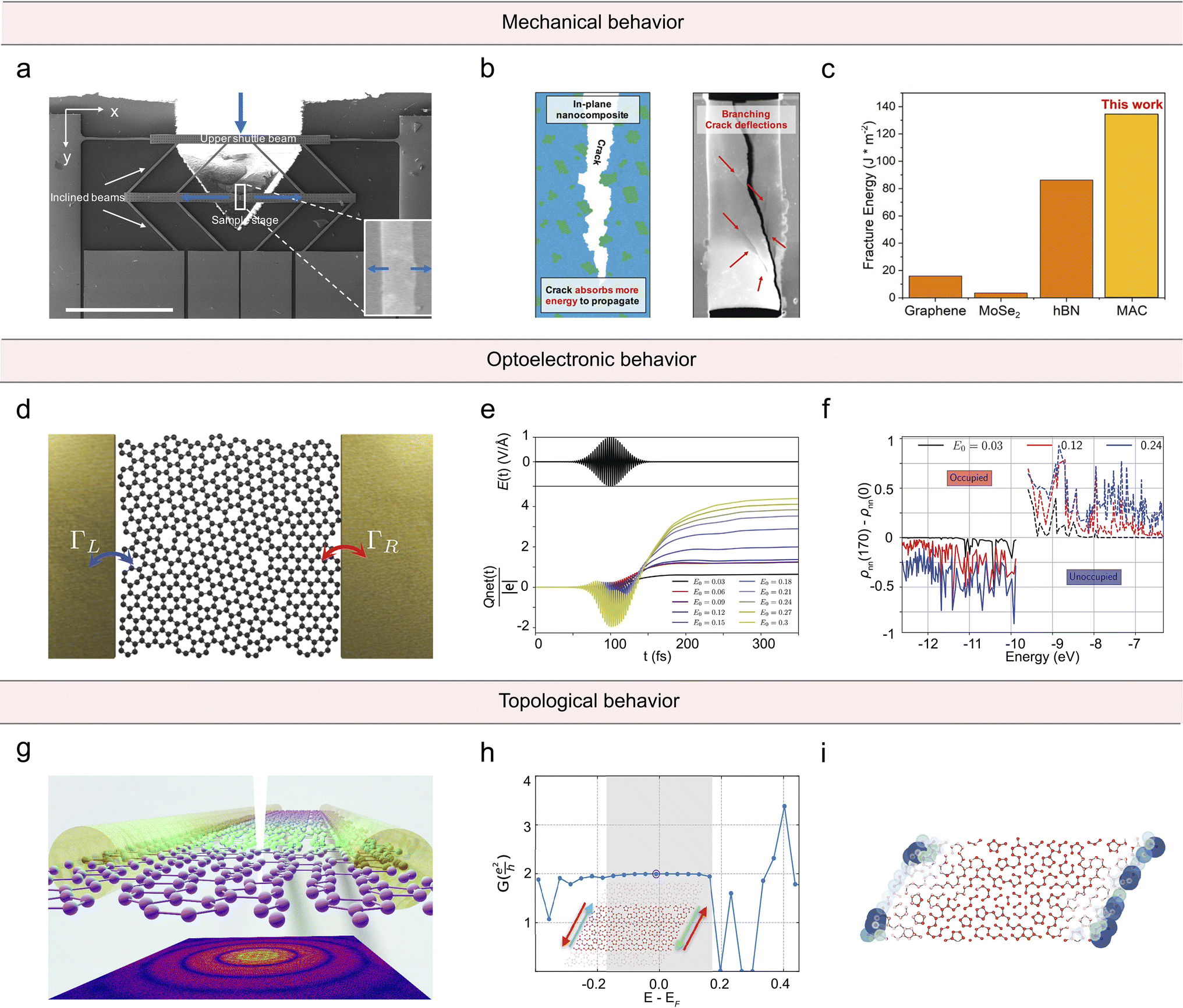 | ||
| Fig. 11 Mechanical, optoelectronic and topological properties of 2D amorphous materials. (a) SEM image of an in situ uniaxial tensile testing microdevice of a MAC film. (b) Schematic of crack deflection by nanocrystalline domains in an amorphous matrix (left); SEM images of fracture branches (red arrows, right). (c) Comparison of the fracture energy of graphene, MoSe2, h-BN, and MAC. It indicates the improved fracture strain and crack stability of MAC. Reproduced with permission.42 Copyright 2025 Elsevier Ltd. (d) Schematic of the metal-MAC-metal junction. This localization leads to different couplings with the left (ΓL) and right (ΓR) electrodes. (e) Laser pulse (upper panel) triggers charge-transfer dynamics in MAC under varying amplitudes (lower panel). (f) Electronic state population increases with E0, involving more states in the current generation. Reproduced with permission.89 Copyright 2022 American Chemical Society. (g) Schematic of the topological insulator properties of amorphous hydrogen half-functionalized bismuthene systems approaching the single-layer limit. (h) Electronic two-terminal conductance, showing the quantization plateau within the topological gap (gray). (i) Wave function spectral weight of one midgap state (purple circle), demonstrating edge-localized topological conductance channels. Reproduced with permission.90 Copyright 2019 American Chemical Society. | ||
Emergent optoelectronic properties also highlight the versatility of single-layer-limit amorphous materials.89,91 For example, Simine et al. simulated a metal-MAC-metal junction using a semiempirical Pariser–Parr–Pople (PPP) Hamiltonian combined with first-principles time-dependent quantum transport theory (Fig. 11d). They observed spatially asymmetric coupling between the amorphous structure and metal electrodes (ΓLvs. ΓR), originating from the localized electronic states in the amorphous material.89 This unique electronic configuration enables the generation of directional electronic currents in unbiased nanojunctions under femtosecond laser irradiation (Fig. 11e). At the same time, the net charge transfer increases with laser intensity, as the higher photon flux at elevated intensities enhances resonant photoexcitation and amplifies orbital population redistribution, as shown in Fig. 11f. This phenomenon is attributed to the inherent disorder-induced orbital localization, suggesting its potential applications in ultrafast optoelectronic devices and optical actuators.
Amorphous materials approaching the single-layer limit can also exhibit topological insulator properties. For instance, hydrogen-functionalized bismuthine, fabricated through the bond-flipping amorphization protocol (Fig. 11g), exhibits a quantized conductance plateau within the energy gap region (Fig. 11h), revealing a quantum spin Hall (QSH) insulating phase.90 Specifically, the site projection of these midgap states evidences two conductive channels located at the edges of the topological material, as shown in Fig. 11i. This finding paves the way for designing topological materials with disordered architectures included, thereby enriching the toolbox for fault-tolerant quantum devices.
5. Conclusion and outlook
The advent of 2D materials and their advanced characterization technologies has enabled the development of amorphous materials with a thickness approaching the single-layer limit, attracting increasing research interest. Interestingly, these atomically thin amorphous systems exhibit unique properties that distinguish them from both their crystalline counterparts and bulk amorphous materials, while retaining the specific characteristics of each. Table 1 summarizes the current achievements in this emerging field, focusing on three aspects: structural parameters, synthesis strategies, and unique properties.| Systems | Materials | Methods | Mechanisms | Properties | Ref. |
|---|---|---|---|---|---|
| Carbon | Carbon | E-beam irradiation | Lattice damage | Decreasing mobility | 40 |
| Carbon | CVD | Pyrolysis temperature | Disorder-tuned conductivity | 25 | |
| Carbon | LCVD | Non-thermodynamic equilibrium | High breaking strength | 26 | |
| Carbon | CVD | Lattice mismatch | Large negative magnetoresistance | 39 | |
| N-doped carbon | Solid templating | Confined polymerization | p-type semiconductor | 24 | |
| Oxides/hydroxides | MoO3 | UV-ozone oxidation | Low temperature | Nonvolatile resistive switching | 46 |
| Ni(OH)2 | Electrochemical conversion | Jahn–Teller distortion | High capacity | 47 | |
| HfO2, Gd2O3, Al2O3 | Oxidation of liquid metal | Self-limiting interfacial oxidation | Ultrathin insulator dielectrics | 28 | |
| GaOxHx, CoOxHx, RhOxHx, etc. | Surfactant templating | Confined hydrolysis | Robust stability | 48 | |
| Metals | Ir, Rh, Ru, etc. | CVD | Alkaline salts and low temperature | High-performance OER | 31 |
| Pd | Wet chemical synthesis | Ligand exchange induction | High HER activity and durability | 55 | |
| Rh; Rh alloy | Wet chemical synthesis | Phase engineering | High selectivity to indole | 56 | |
| Cu | DNA template | Limited area growth | Stronger photoemission and photostability | 54 | |
| TMDCs | VS2 | Supercritical pressure | Strain engineering | High photoluminescence and photothermal conversion efficiency | 57 |
| PtSex | Deep reactive ion etching | Low-temperature etching | High atom-utilization efficiency in the HER | 29 | |
| MoS2 | Grazing ion irradiation | Lattice damage | Metallic electronic properties | 58 | |
| MOFs/COFs | HE-MOF (Ru, Mo) | One-pot synthesis | Inducing electron redistribution | Enhanced OER | 69 |
| MOF (Cu, Au, Co) | Self-assembly | Stoichiometric ratio and annealing temperature | Angularly changeable intermolecular links | 68 | |
| MOF (Pd) | Sequential deposition | Solvent regulation | Good chemical stability | 71 | |
| PDBA | Solution polymerization | Dynamic step-by-step aggregation | Dynamic structural fluctuation | 70 | |
| Potential | BP | Pulsed laser deposition | Low-temperature laser deposition | High hole mobility | 92 |
| Se-alloyed Te-TeOx | Thermal evaporation | Embeddedness and dispersion | High-performance stable p-channel | 33 | |
| BN | Remote ICP-CVD | Plasma enhancement | Ultralow dielectric constant | 74 | |
| SiO2 | Surfactant templating | Interlayer molecular modification | High specific surface areas | 93 |
They have brought two key advantages to the current field: (i) fundamental structural insights. Their atomic-scale thickness makes it achievable to extract their key structural parameters—including local bonding configurations and topological disorder—through advanced technologies like STEM imaging. The ability to directly visualize and quantify these parameters at the atomic level provides new opportunities to establish structure–property relationships in disordered systems. This represents a significant advancement over bulk amorphous materials; (ii) unique and tunable properties, beyond those of their crystalline counterparts. Electrically, they can span a wide range across insulating, semiconducting, and metallic states, with the ability to undergo smooth transitions between these states through compositional and structural modifications. Electrochemically, they also demonstrate superior catalytic activities for the HER and OER, attributed to abundant unsaturated coordination sites and optimized surface reaction kinetics. Furthermore, other fantastic properties, exemplified by enhanced robustness, novel optoelectronic characteristics, and emergent quantum phenomena, have been evidenced, fundamentally arising from their disordered structure.
Although remarkable progress has been achieved in single-layer-limit amorphous materials, the field remains in its early stages. We here provide our personal views on the current challenges and possible prospects in this emerging field, as shown in Fig. 12.
 | ||
| Fig. 12 Challenges and prospects of amorphous materials when approaching the single-layer limit. The five promising directions in this emergent field: (i) expansion of the library of the single-layer-limit amorphous materials; (ii) encapsulation and interface design for the stability; (iii) growth mechanistic analysis through in situ characterization and thermodynamic simulation; (iv) optimization of modeling and theoretical calculations; (v) exploration of applications in flexible electronics and neuromorphic computing. | ||
5.1. Challenges
5.2. Opportunities
Author contributions
Y. H. conceived the concept and outlined the article. Y. H. also supervised the completion of the manuscript. Z. S. and H. G. conducted the literature review and drafted the manuscript. All authors participated in discussions and refined the manuscript.Conflicts of interest
The authors declare no conflict of interest.Data availability
No primary research results, software or code have been included and no new data were generated or analyzed as part of this review.Acknowledgements
This work was financially supported by the open research fund of Songshan Lake Materials Laboratory (2023SLABFN08), the National Natural Science Foundation of China (52203354 and 22272048), the National Natural Science Fund for Excellent Young Scientists Fund Program (Overseas), the Fundamental Research Funds for the Central Universities (531119200209), the National Key R&D Program of China (2021YFA1500900), the Natural Science Foundation of Hunan Province of China (2023JJ10004), The Science and Technology innovation Program of Hunan Province (2024RC3081) and Guangdong Basic and Applied Basic Research Foundation (2023A1515012648).References
- J. Kang, X. Yang, Q. Hu, Z. Cai, L.-M. Liu and L. Guo, Chem. Rev., 2023, 123, 8859–8941 CrossRef CAS PubMed.
- H. Lan, J. Wang, L. Cheng, D. Yu, H. Wang and L. Guo, Chem. Soc. Rev., 2024, 53, 684–713 RSC.
- B. Wang, G. M. Biesold, M. Zhang and Z. Lin, Chem. Soc. Rev., 2021, 50, 6914–6949 RSC.
- J. Liu, R. Hao, B. Jia, H. Zhao and L. Guo, Nanomaterials, 2021, 11, 3246 CrossRef CAS PubMed.
- Z. Guo, Z. Liu and R. Tang, Mater. Chem. Front., 2024, 8, 1703–1730 RSC.
- Z. Li, B. Li, M. Yu, C. Yu and P. Shen, Int. J. Hydrogen Energy, 2022, 47, 26956–26977 CrossRef.
- J. F. von Liebig and L. P. B. Playfair, Organic chemistry in its applications to agriculture and physiology, J. Owen, 1841, 436–447 Search PubMed.
- J. Kramer, Ann. Phys., 1934, 411, 37–64 CrossRef.
- W. Klement, R. H. Willens and P. O. L. Duwez, Nature, 1960, 187, 869–870 CrossRef CAS.
- N. Cherradi, A. Audouard, A. Kazoun and G. Marchal, Solid State Commun., 1989, 70, 315–319 CrossRef CAS.
- A. Inoue, Acta Mater., 2000, 48, 279–306 CrossRef CAS.
- A. Hirata, P. Guan, T. Fujita, Y. Hirotsu, A. Inoue, A. R. Yavari, T. Sakurai and M. Chen, Nat. Mater., 2011, 10, 28–33 CrossRef CAS.
- L. Lin, B. Deng, J. Sun, H. Peng and Z. Liu, Chem. Rev., 2018, 118, 9281–9343 CrossRef CAS PubMed.
- A. R. Choi, D. H. Lim, S.-Y. Shin, H. J. Kang, D. Kim, J.-Y. Kim, Y. Ahn, S. W. Ryu and I.-K. Oh, Chem. Mater., 2024, 36, 2194–2219 CrossRef CAS.
- W. Li, J. Zhou, S. Cai, Z. Yu, J. Zhang, N. Fang, T. Li, Y. Wu, T. Chen, X. Xie, H. Ma, K. Yan, N. Dai, X. Wu, H. Zhao, Z. Wang, D. He, L. Pan, Y. Shi, P. Wang, W. Chen, K. Nagashio, X. Duan and X. Wang, Nat. Electron., 2019, 2, 563–571 CrossRef CAS.
- Z. Hu, X. Xiao, H. Jin, T. Li, M. Chen, Z. Liang, Z. Guo, J. Li, J. Wan, L. Huang, Y. Zhang, G. Feng and J. Zhou, Nat. Commun., 2017, 8, 15630 CrossRef CAS.
- S. Manzeli, D. Ovchinnikov, D. Pasquier, O. V. Yazyev and A. Kis, Nat. Rev. Mater., 2017, 2, 17033 CrossRef CAS.
- A. Lebedev, Tr. Gos. Opt. Inst., 1921, 2, 1–20 Search PubMed.
- T. Ge, W. Cui and Q. Xu, Angew. Chem., Int. Ed., 2023, 62, e202300446 CrossRef CAS PubMed.
- H. W. Zhao, X. J. Chen, G. Z. Wang, Y. F. Qiu and L. Guo, 2D Mater., 2019, 6, 032002 CrossRef.
- S.-B. Duan, Y.-Q. Wang, R. Cao, Y.-F. Sun, W. Zhang and R.-M. Wang, Rare Met., 2025, 44, 822–840 CrossRef CAS.
- H. Jang, H. Kim, G. Kim, S. Cho and H. Yang, Nano Convergence, 2024, 11, 46 CrossRef CAS PubMed.
- J.-Q. Zhong and H.-J. Freund, Chem. Rev., 2022, 122, 11172–11246 CrossRef CAS PubMed.
- X. Bai, P. Hu, A. Li, Y. Zhang, A. Li, G. Zhang, Y. Xue, T. Jiang, Z. Wang, H. Cui, J. Kang, H. Zhao, L. Gu, W. Zhou, L.-M. Liu, X. Qiu and L. Guo, Nature, 2024, 634, 80–84 CrossRef CAS PubMed.
- H. Tian, Y. Ma, Z. Li, M. Cheng, S. Ning, E. Han, M. Xu, P.-F. Zhang, K. Zhao, R. Li, Y. Zou, P. Liao, S. Yu, X. Li, J. Wang, S. Liu, Y. Li, X. Huang, Z. Yao, D. Ding, J. Guo, Y. Huang, J. Lu, Y. Han, Z. Wang, Z. G. Cheng, J. Liu, Z. Xu, K. Liu, P. Gao, Y. Jiang, L. Lin, X. Zhao, L. Wang, X. Bai, W. Fu, J.-Y. Wang, M. Li, T. Lei, Y. Zhang, Y. Hou, J. Pei, S. J. Pennycook, E. Wang, J. Chen, W. Zhou and L. Liu, Nature, 2023, 615, 56–61 CrossRef CAS.
- W. H. Zachariasen, J. Am. Chem. Soc., 1932, 54, 3841–3851 CrossRef CAS.
- M. Kong, M. H. Vong, M. Kwak, I. Lim, Y. Lee, S.-h. Lee, I. You, O. Awartani, J. Kwon, T. J. Shin, U. Jeong and M. D. Dickey, Science, 2024, 385, 731–737 CrossRef PubMed.
- A. Zavabeti, J. Z. Ou, B. J. Carey, N. Syed, R. Orrell-Trigg, E. L. H. Mayes, C. Xu, O. Kavehei, A. P. O'Mullane, R. B. Kaner, K. Kalantar-zadeh and T. Daeneke, Science, 2017, 358, 332–335 CrossRef.
- Y. He, L. Liu, C. Zhu, S. Guo, P. Golani, B. Koo, P. Tang, Z. Zhao, M. Xu, C. Zhu, P. Yu, X. Zhou, C. Gao, X. Wang, Z. Shi, L. Zheng, J. Yang, B. Shin, J. Arbiol, H. Duan, Y. Du, M. Heggen, R. E. Dunin-Borkowski, W. Guo, Q. J. Wang, Z. Zhang and Z. Liu, Nat. Catal., 2022, 5, 212–221 CrossRef CAS.
- W. Xu, Y. Wu, S. Xi, Y. Wang, Y. Wang, Y. Ke, L. Ding, X. Wang, J. Yang, W. Zhang, K. P. Loh, F. Ding, Z. Liu and M. Chhowalla, Nat. Synth., 2025, 4, 327–335 CrossRef CAS PubMed.
- G. Wu, X. Zheng, P. Cui, H. Jiang, X. Wang, Y. Qu, W. Chen, Y. Lin, H. Li, X. Han, Y. Hu, P. Liu, Q. Zhang, J. Ge, Y. Yao, R. Sun, Y. Wu, L. Gu, X. Hong and Y. Li, Nat. Commun., 2019, 10, 4855 CrossRef PubMed.
- Y. Liu, A. Madanchi, A. S. Anker, L. Simine and V. L. Deringer, Nat. Rev. Mater., 2024, 228–241 CrossRef.
- A. Liu, Y.-S. Kim, M. G. Kim, Y. Reo, T. Zou, T. Choi, S. Bai, H. Zhu and Y.-Y. Noh, Nature, 2024, 629, 798–802 CrossRef CAS.
- D. Chen, H. Zhuang, M. Chen, P. Y. Huang, V. Vlcek and Y. Jiao, Appl. Phys. Rev., 2023, 10, 021310 CAS.
- D. Chen, Y. Zheng, L. Liu, G. Zhang, M. Chen, Y. Jiao and H. Zhuang, Proc. Natl. Acad. Sci. U.S.A., 2021, 118, e2016862118 CrossRef CAS.
- Y. Zheng, L. Liu, H. Q. Nan, Z. X. Shen, G. Zhang, D. Y. Chen, L. X. He, W. X. Xu, M. Chen, Y. Jiao and H. L. Zhuang, Sci. Adv., 2020, 6, eaba0826 CrossRef CAS PubMed.
- Y. van de Burgt, J. Laser Appl., 2014, 26, 032001 CrossRef.
- F. An, C. Wang, V. H. Pham, A. Borisevich, J. Qian, K. Yin, S. Pidaparthy, B. Robinson, A.-S. Chou, J. Lee, J. Weidman, S. Natesakhawat, H. Wang, A. Schleife, J.-M. Zuo, C. Matranga and Q. Cao, Commun. Eng., 2023, 2, 93 CrossRef.
- W.-J. Joo, J.-H. Lee, Y. Jang, S.-G. Kang, Y.-N. Kwon, J. Chung, S. Lee, C. Kim, T.-H. Kim, C.-W. Yang, U. J. Kim, B. L. Choi, D. Whang and S.-W. Hwang, Sci. Adv., 2017, 3, e1601821 CrossRef PubMed.
- M. Z. Iqbal, O. Kelekci, M. W. Iqbal and J. Eom, Carbon, 2013, 59, 366–371 CrossRef CAS.
- D. Propst, W. Joudi, M. Längle, J. Madsen, C. Kofler, B. M. Mayer, D. Lamprecht, C. Mangler, L. Filipovic, T. Susi and J. Kotakoski, Sci. Rep., 2024, 14, 26939 CrossRef PubMed.
- B. Shin, B. Ni, C.-T. Toh, D. Steinbach, Z. Yang, L. M. Sassi, Q. Ai, K. Niu, J. Lin, K. Suenaga, Y. Han, M. J. Buehler, B. Özyilmaz and J. Lou, Matter, 2025, 8, 102000 CrossRef.
- X. Zhang, Y.-T. Zhang, Y.-P. Wang, S. Li, S. Du, Y.-Y. Zhang and S. T. Pantelides, Phys. Rev. B, 2024, 109, 174106 CrossRef CAS.
- Z. Li, H. Tian, S. U, X. Huang, M. Cheng, X. Han, Y. Ma, P. Liao, Z. Yao, Y. Wang, L. Y. Zhang, G. Yin, Y. Luo, W. Li, X. Zhang, J. Guo, X. Zhao, L. Wang, J. Chen and L. Liu, Adv. Funct. Mater., 2025, 2424751 CrossRef CAS.
- E. Griffin, L. Mogg, G.-P. Hao, G. Kalon, C. Bacaksiz, G. Lopez-Polin, T. Y. Zhou, V. Guarochico, J. Cai, C. Neumann, A. Winter, M. Mohn, J. H. Lee, J. Lin, U. Kaiser, I. V. Grigorieva, K. Suenaga, B. Özyilmaz, H.-M. Cheng, W. Ren, A. Turchanin, F. M. Peeters, A. K. Geim and M. Lozada-Hidalgo, ACS Nano, 2020, 14, 7280–7286 CrossRef CAS PubMed.
- M. H. Alam, S. Chowdhury, A. Roy, X. Wu, R. Ge, M. A. Rodder, J. Chen, Y. Lu, C. Stern, L. Houben, R. Chrostowski, S. R. Burlison, S. J. Yang, M. I. Serna, A. Dodabalapur, F. Mangolini, D. Naveh, J. C. Lee, S. K. Banerjee, J. H. Warner and D. Akinwande, ACS Nano, 2022, 16, 3756–3767 CrossRef CAS PubMed.
- J. Kang, Y. Xue, J. Yang, Q. Hu, Q. Zhang, L. Gu, A. Selloni, L. M. Liu and L. Guo, J. Am. Chem. Soc., 2022, 144, 8969–8976 CrossRef CAS PubMed.
- E. Yamamoto, D. Kurimoto, K. Ito, K. Hayashi, M. Kobayashi and M. Osada, Nat. Commun., 2024, 15, 6612 CrossRef CAS PubMed.
- M. Lee, G. Yoon, M. K. Kim, J. Hong, S. Lee and G. H. Ryu, J. Alloys Compd., 2024, 976, 173282 CrossRef.
- K. Yi, W. Qin, Y. Huang, Y. Wu, S. Feng, Q. Fang, X. Cao, Y. Deng, C. Zhu, X. Zou, K.-W. Ang, T. Li, X. Wang, J. Lou, K. Lai, Z. Hu, Z. Zhang, Y. Dong, K. Kalantar-Zadeh and Z. Liu, Nat. Electron., 2024, 7, 1126–1136 CrossRef.
- A. Malasi, H. Taz, A. Farah, M. Patel, B. Lawrie, R. Pooser, A. Baddorf, G. Duscher and R. Kalyanaraman, Sci. Rep., 2015, 5, 18157 CrossRef.
- Y. Chen, Z. Fan, Z. Zhang, W. Niu, C. Li, N. Yang, B. Chen and H. Zhang, Chem. Rev., 2018, 118, 6409–6455 CrossRef CAS.
- J. Zhao, L. Li, P. Li, L. Dai, J. Dong, L. Zhou, Y. Wang, P. Zhang, K. Ji, Y. Zhang, H. Yu, Z. Wei, J. Li, X. Li, Z. Huang, B. Wang, J. Liu, Y. Chen, X. Zhang, S. Wang, N. Li, W. Yang, D. Shi, J. Pan, S. Du, L. Du and G. Zhang, Nature, 2025, 639, 354–359 CrossRef CAS PubMed.
- X. Ouyang, Y. Wu, Y. Gao, L. Li, L. Li, T. Liu, X. Jing, Y. Fu, J. Luo, G. Xie, S. Jia, M. Li, Q. Li, C. Fan and X. Liu, J. Am. Chem. Soc., 2023, 145, 4553–4563 CrossRef CAS PubMed.
- H. Cheng, N. Yang, G. Liu, Y. Ge, J. Huang, Q. Yun, Y. Du, C. J. Sun, B. Chen, J. Liu and H. Zhang, Adv. Mater., 2020, 32, 1902964 CrossRef CAS PubMed.
- J. Ge, P. Yin, Y. Chen, H. Cheng, J. Liu, B. Chen, C. Tan, P. F. Yin, H. X. Zheng, Q. Q. Li, S. Chen, W. Xu, X. Wang, G. Wu, R. Sun, X. H. Shan, X. Hong and H. Zhang, Adv. Mater., 2021, 33, 2006711 CrossRef CAS.
- Y. Zhou, Q. Xu, T. Ge, X. Zheng, L. Zhang and P. Yan, Angew. Chem., Int. Ed., 2020, 59, 3322–3328 CrossRef CAS PubMed.
- P. Valerius, S. Kretschmer, B. V. Senkovskiy, S. Wu, J. Hall, A. Herman, N. Ehlen, M. Ghorbani-Asl, A. Grüneis, A. V. Krasheninnikov and T. Michely, 2D Mater., 2020, 7, 025005 CrossRef CAS.
- J. J. Pyeon, S. H. Kim, D. S. Jeong, S.-H. Baek, C.-Y. Kang, J.-S. Kim and S. K. Kim, Nanoscale, 2016, 8, 10792–10798 RSC.
- B. C. Bayer, R. Kaindl, M. Reza Ahmadpour Monazam, T. Susi, J. Kotakoski, T. Gupta, D. Eder, W. Waldhauser and J. C. Meyer, ACS Nano, 2018, 12, 8758–8769 CrossRef CAS PubMed.
- Z. Shi, W. Qin, Z. Hu, M. Ma, H. Liu, Z. Shu, Y. Jiang, H. Xia, W. Shi, C. Y. Zhang, X. Sang, C. Guo, Y. Li, C. Liu, C. Gong, H. Wang, S. Liu, L. Tapasztó, C. Gao, F. Liu, P. Tang, Y. Liu, H. Duan, E. Xie, Z. Zhang, Z. Liu and Y. He, Nat. Mater., 2025, 24, 1186–1194 CrossRef CAS PubMed.
- Y. Shi, J. Pu and L. Wang, J. Phys. Chem. C, 2020, 125, 836–844 CrossRef.
- W. Zhao, C. Cui, Y. Xu, Q. Liu, Y. Zhang, Z. Zhang, S. Lu, Z. Rong, X. Li, Y. Fang and W. Huang, Adv. Mater., 2023, 35, 2301593 CrossRef CAS PubMed.
- J. Duan, Y. Li, Y. Pan, N. Behera and W. Jin, Coord. Chem. Rev., 2019, 395, 25–45 CrossRef CAS.
- Z.-B. Zhou, H.-H. Sun, Q.-Y. Qi and X. Zhao, Angew. Chem., Int. Ed., 2023, 62, e202305131 CrossRef CAS PubMed.
- J. Li, Z. Cheng, Z. Wang, J. Dong, H. Jiang, W. Wang, X. Zou and G. Zhu, Angew. Chem., Int. Ed., 2023, 62, e202216675 CrossRef CAS PubMed.
- J. Lu, H. Jiang, Y. Yan, Z. Zhu, F. Zheng and Q. Sun, ACS Nano, 2022, 16, 13160–13167 CrossRef CAS PubMed.
- J. Lu, D. Nieckarz, H. Jiang, Z. Zhu, Y. Yan, F. Zheng, W. Rżysko, J. Lisiecki, P. Szabelski and Q. Sun, ACS Nano, 2023, 17, 20194–20202 CrossRef CAS PubMed.
- X. Mu, M. Yu, X. Liu, Y. Liao, F. Chen, H. Pan, Z. Chen, S. Liu, D. Wang and S. Mu, ACS Energy Lett., 2024, 9, 5763–5770 CrossRef CAS.
- G. Zhan, Z. F. Cai, K. Strutynski, L. Yu, N. Herrmann, M. Martinez-Abadia, M. Melle-Franco, A. Mateo-Alonso and S. Feyter, Nature, 2022, 603, 835–840 CrossRef PubMed.
- A. Cucinotta, S. Eyley, J. A. Davies, W. Thielemans, K. S. Mali and S. De Feyter, J. Am. Chem. Soc., 2025, 147, 7682–7693 CrossRef CAS PubMed.
- Q. Fang, K. Yi, T. Zhai, S. Luo, C.-y. Lin, Q. Ai, Y. Zhu, B. Zhang, G. A. Alvarez, Y. Shao, H. Zhou, G. Gao, Y. Liu, R. Xu, X. Zhang, Y. Wang, X. Tian, H. Zhang, Y. Han, H. Zhu, Y. Zhao, Z. Tian, Y. Zhong, Z. Liu and J. Lou, Nat. Commun., 2024, 15, 10780 CrossRef CAS.
- L. Lichtenstein, M. Heyde and H.-J. Freund, J. Phys. Chem. C, 2012, 116, 20426–20432 CrossRef CAS.
- S. Hong, C.-S. Lee, M.-H. Lee, Y. Lee, K. Y. Ma, G. Kim, S. I. Yoon, K. Ihm, K.-J. Kim, T. J. Shin, S. W. Kim, E.-c. Jeon, H. Jeon, J.-Y. Kim, H.-I. Lee, Z. Lee, A. Antidormi, S. Roche, M. Chhowalla, H.-J. Shin and H. S. Shin, Nature, 2020, 582, 511–514 CrossRef CAS.
- E. I. Altman and P. Dementyev, Catal. Lett., 2024, 154, 1359–1374 CrossRef CAS.
- C. Büchner and M. Heyde, Prog. Surf. Sci., 2017, 92, 341–374 CrossRef.
- Y. Gao, S. Wang, J. Jiang, Y. Liu, J. S. Francisco and X. C. Zeng, J. Am. Chem. Soc., 2024, 146, 2503–2513 CrossRef CAS PubMed.
- Z. Lu, M. Zhu, Y. Liu, G. Zhang, Z. Tan, X. Li, S. Xu, L. Wang, R. Dou, B. Wang, Y. Yao, Z. Zhang, J. Dong, Z. Cheng and S. Chen, ACS Appl. Mater. Interfaces, 2022, 14, 25984–25992 CrossRef CAS.
- C. Y. Chen, Z. Sun, R. Torsi, K. Wang, J. Kachian, B. Liu, G. B. Rayner, Z. Chen, J. Appenzeller, Y.-C. Lin and J. A. Robinson, Nat. Commun., 2024, 15, 4016 CrossRef CAS PubMed.
- S. M. Sattari-Esfahlan, S. Mirzaei, M. J. Josline, J.-Y. Moon, S.-H. Hyun, H. Jang and J.-H. Lee, Nano Convergence, 2025, 12, 22 CrossRef PubMed.
- C. Liu, X. Li, Y. Wang, Z. Zheng, B. Wu, W. He, X. Dong, Z. Zhang, B. Chen, J. Huang, Z. An, C. Zheng, G. Huang and Y. Mei, Nat. Commun., 2025, 16, 150 CrossRef.
- R. Li, Z. Yao, Z. Li, L. Liao, H. Sun, C. Cong, X. Huang, K. Wu, T. Wang, H. Tian, P. Liao, S. Liu, Y. Wang, L. Yang Zhang, U. Sasaki, G. Yin, J. Guo, Y. Ye, X. Wei, X. Wang, J. Hong, J. Mao, L. Bao, L. Wang, X. Bai, P. Gao, K. Liu, L. Liao, J. He, S. Bai, Y. Zhang, Y. Hou, R. Zou, H.-J. Gao, Y. Zhang, E. Wang and L. Liu, Nat. Synth., 2024, 4, 106–115 CrossRef.
- G. Modi, S. K. Parate, C. Kwon, A. C. Meng, U. Khandelwal, A. Tullibilli, J. Horwath, P. K. Davies, E. A. Stach, J. Li, P. Nukala and R. Agarwal, Nature, 2024, 635, 847–853 CrossRef PubMed.
- S. Moon, D. Lee, J. Park and J. Kim, ACS Appl. Mater. Interfaces, 2023, 15, 37687–37695 CrossRef CAS.
- P. Berggren and J. Fransson, Phys. Rev. B:Condens. Matter Mater. Phys., 2015, 91, 205438 CrossRef.
- W. Wang, J. Qi, Z. Wu, W. Zhai, Y. Pan, K. Bao, L. Zhai, J. Wu, C. Ke, L. Wang, M. Ding and Q. He, Nat. Protoc., 2023, 18, 2891–2926 CrossRef CAS PubMed.
- M. A. Klatt, P. J. Steinhardt and S. Torquato, Proc. Natl. Acad. Sci. U. S. A., 2022, 119, e2213633119 CrossRef CAS PubMed.
- E. J. A. Dos Santos, M. L. J. Pereira, R. M. Tromer, D. S. Galvao and L. A. J. Ribeiro, Nanoscale, 2025, 17, 7253–7263 RSC.
- A. J. Garzón-Ramírez, N. Gastellu and L. Simine, J. Phys. Chem. Lett., 2022, 13, 1057–1062 CrossRef PubMed.
- M. Costa, G. R. Schleder, M. Buongiorno Nardelli, C. Lewenkopf and A. Fazzio, Nano Lett., 2019, 19, 8941–8946 CrossRef CAS PubMed.
- H. Seung, J. Bok, J. S. Kim, J. Kim, H. Choi, J. Ahn, J. P. Hong, E. Yoon, S. Blumstengel, Y. Y. Kim, L. Colazzo, S. Park, D. K. Hwang, J. Park, C. Choi, T. Hyeon and D.-H. Kim, Nat. Synth., 2025, 4, 514–522 CrossRef CAS.
- Z. Yang, J. Hao, S. Yuan, S. Lin, H. M. Yau, J. Dai and S. P. Lau, Adv. Mater., 2015, 27, 3748–3754 CrossRef PubMed.
- Y. Takeuchi, S. Obata, K. Ohkura and Y. Nishina, ACS Mater. Lett., 2022, 4, 2590–2596 CrossRef CAS.
- A. Madanchi, E. Azek, K. Zongo, L. K. Beland, N. Mousseau and L. Simine, ACS Phys. Chem. Au, 2025, 5, 3–16 CrossRef CAS.
- G. Jung, R. M. Alkemade, V. Bapst, D. Coslovich, L. Filion, F. P. Landes, A. J. Liu, F. S. Pezzicoli, H. Shiba, G. Volpe, F. Zamponi, L. Berthier and G. Biroli, Nat. Rev. Phys., 2025, 7, 91–104 CrossRef.
- Y. Yang, J. Zhou, F. Zhu, Y. Yuan, D. J. Chang, D. S. Kim, M. Pham, A. Rana, X. Tian, Y. Yao, S. J. Osher, A. K. Schmid, L. Hu, P. Ercius and J. Miao, Nature, 2021, 592, 60–64 CrossRef CAS.
- X. Lyu, G. Wu, Z. Zheng, S. Xia, J. Xie, Y. Xia, P. Fan, R. Zhu, Y. Wang, D. Yang, T. Li and A. Dong, ACS Nano, 2024, 18, 2219–2230 CrossRef CAS PubMed.
- K. Yi, Y. Wu, L. An, Y. Deng, R. Duan, J. Yang, C. Zhu, W. Gao and Z. Liu, Adv. Mater., 2024, 36, 2403494 CrossRef CAS PubMed.
- Z. Lin, C. Du, B. Yan, C. Wang and G. Yang, Nat. Commun., 2018, 9, 4036 CrossRef.
- Z. Sun, B. Zhang, M. Khurram and Q. Yan, 2D Mater., 2022, 9, 025019 CrossRef CAS.
- H. Zhu, S. Yan, S. Xiong and X. Wu, Cryst. Growth Des., 2017, 17, 5608–5613 CrossRef CAS.
- C. Chang, L. Wang, L. Xie, W. Zhao, S. Liu, Z. Zhuang, S. Liu, J. Li, X. Liu and Q. Zhao, Nano Res., 2022, 15, 8613–8635 CrossRef CAS.
- Y.-T. Zhang, Y.-P. Wang, X. Zhang, Y.-Y. Zhang, S. Du and S. T. Pantelides, Nano Lett., 2022, 22, 8018–8024 CrossRef CAS PubMed.
- Y. Wei, Y. Xu, H. Zhang, J. Jiang and Q. Xu, New J. Chem., 2024, 48, 11206–11210 RSC.
- H. Mei, Y. Zhang, P. Zhang, A. G. Ricciardulli, P. Samorì and S. Yang, Adv. Sci., 2024, 11, 2409404 CrossRef PubMed.
- Y. Sun and S. Dai, Nat. Synth., 2024, 3, 1457–1470 CrossRef CAS.
- G. Kim, B. Huet, C. E. Stevens, K. Jo, J.-Y. Tsai, S. Bachu, M. Leger, S. Song, M. Rahaman, K. Y. Ma, N. R. Glavin, H. S. Shin, N. Alem, Q. Yan, J. R. Hendrickson, J. M. Redwing and D. Jariwala, Nat. Commun., 2024, 15, 6361 CrossRef CAS PubMed.
- M. Liebich, M. Florian, N. Nilforoushan, F. Mooshammer, A. D. Koulouklidis, L. Wittmann, K. Mosina, Z. Sofer, F. Dirnberger, M. Kira and R. Huber, Nat. Mater., 2025, 24, 384–390 CrossRef CAS.
- S. Lan, L. Zhu, Z. Wu, L. Gu, Q. Zhang, H. Kong, J. Liu, R. Song, S. Liu, G. Sha, Y. Wang, Q. Liu, W. Liu, P. Wang, C.-T. Liu, Y. Ren and X.-L. Wang, Nat. Mater., 2021, 20, 1347–1352 CrossRef CAS.
- D. Won, J. Bang, S. H. Choi, K. R. Pyun, S. Jeong, Y. Lee and S. H. Ko, Chem. Rev., 2023, 123, 9982–10078 CrossRef CAS.
- A. Abbas, Y. Luo, W. Ahmad, M. Mustaqeem, L. Kong, J. Chen, G. Zhou, T. A. Tabish, Q. Zhang and Q. Liang, Nano Today, 2024, 56, 102256 CrossRef.
- I. Boybat, M. Le Gallo, S. R. Nandakumar, T. Moraitis, T. Parnell, T. Tuma, B. Rajendran, Y. Leblebici, A. Sebastian and E. Eleftheriou, Nat. Commun., 2018, 9, 2514 CrossRef PubMed.
- G. Ding, H. Li, J. Zhao, K. Zhou, Y. Zhai, Z. Lv, M. Zhang, Y. Yan, S.-T. Han and Y. Zhou, Chem. Rev., 2024, 124, 12738–12843 CrossRef CAS PubMed.
Footnote |
| † These authors contributed equally: Zude Shi and Haowei Ge. |
| This journal is © The Royal Society of Chemistry 2025 |