 Open Access Article
Creative Commons Attribution 3.0 Unported Licence
Towards sustainable and efficient p-type metal oxide semiconductor materials in dye-sensitised photocathodes for solar energy conversion
Sina
Wrede
 and
Haining
Tian
 *
*
Department of Chemistry-Ångström Lab., Uppsala University, Box 523, 75120 Uppsala, Sweden. E-mail: haining.tian@kemi.uu.se
First published on 27th May 2020
Abstract
In order to meet the ever-growing global energy demand for affordable and clean energy, it is essential to provide this energy by renewable resources and consider the eco-efficiency of the production and abundance of the utilised materials. While this is seldom discussed in the case of technologies still in the research stage, addressing the issue of sustainability is key to push research in the right direction. Here we provide an overview of the current p-type metal oxide semiconductor materials in dye-sensitised photocathodes, considering element abundance, synthetic methods and large scale fabrication as well as the underlying physical properties that are necessary for efficient solar harvesting devices.
1 Introduction
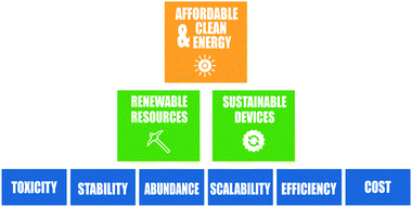
Today, concerns surrounding the causes and consequences of man-made climate changes are central topics in our everyday lives. The global attention to this issue has increased drastically and the demand for a sustainable future is now larger than ever. In order to make such a future our reality, society has to make the transition from fossil-fuel resources to sustainable renewable energy alternatives and cope with the steadily increasing energy demand at the same time. It is predicted that the global energy demand is going to double by 2050 with the main contribution coming from the rise of developing countries.1,2 In particular, Asia is at the forefront due to the economic growth, infrastructure development, population growth and access to electricity for a new segment of the population. In order to achieve a socially just and equitable future, it is imperative that this increase is to be met with a sustainable solution allowing developing countries to increase their living standards.Out of the several renewable energy sources, such as wind, tidal or biomass energy, solar energy is one of the most promising resources due to its abundance and omnipresence. It is estimated that the world's total energy use equals only approximately 0.00015% of the solar energy reaching the earth.3 Furthermore, solar energy can be converted into both electricity and fuels, which makes its storage and transport over long distances easier. In order to fully transit into a carbon free future, the development of solar harvesting is inevitable and needs to reach large-scale deployment, taking the scalability, safety, efficiency and durability into consideration, as illustrated in Fig. 1. Most of the research today focuses mostly on improving the efficiency of devices without taking other selection parameters into consideration. However, the energy demand during production, durability and cost of maintenance of the system can mitigate or compensate extra costs and are therefore important factors to keep in mind during the development of new solar cell and solar fuel devices.
In this perspective, the concept of sustainability is discussed within the field of solar harvesting for solar cells and solar fuel devices with a focus on photocathodes by discussing the current semiconductor materials and their energy costs to identify sustainable electrode candidates considering element abundance, costs and toxicity.
2 Dye sensitised photocathodes for solar cells and solar fuels
Like any other emerging technology in our economy centred society, the success of solar harvesting devices depends mostly on the production costs which are determined by the fabrication process and material costs. While the material costs are mostly driven by the material abundance, it is also important to consider the sustainability and renewability of materials that are used in devices with such a large market and volume in the upcoming years.2.1 Element abundance and life cycle assessment
With a predicted power demand of around 30 TW by 2050,4 solar harvesting devices will have to expand drastically to meet this energy demand. However, terawatt-scale realisation requires a massive amount of natural resources which can prevent reaching this scale due to limited resource supply.5 For current solar cell technologies, Tao et al.5 examined the resource limitations that would arise for the terawatt-scale in order to meet a fraction of our power demand from solar energy harvesting. For example, the terawatt-scale for CIGS or CIS (CuInxGa1−xSe2) solar cells will be hindered by the limited indium reserves, as well as a production bottleneck for gallium, which only exists in very small concentrations in other ores.5 CdTe solar cells will be limited by the availability of tellurium, and the current silicon solar cell technology at such a scale would deplete the silver reserves in only two decades according to Tao (for silver electrodes). This underlines the importance of making the existing technologies more sustainable and exploring new alternatives. For dye-sensitised solar cells, consisting mostly of TiO2 or NiO, which are vastly earth abundant, resource limitations are less critical, especially if an organic dye instead of a ruthenium containing dye is utilised. Most affected by natural resource limitations are materials that use metals that are at supply risk, which often are available largely as byproducts and possess no effective substitutes, as shown in Fig. 2.6 It should be kept in mind that forecasting the availability of materials is not easy and fluctuations can occur, nonetheless, metal availability is a key factor to consider for solar harvesting technologies that are aimed at large-scale production. However, due to the need for the large-scale production of a variety of solar harvesting devices, there is no doubt that some elements that are considered “critical” will be unavoidable and recycling will become more important than ever.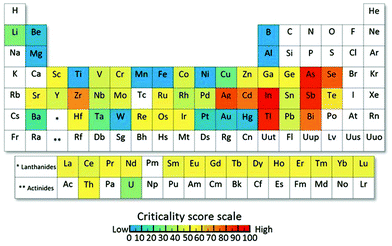 | ||
| Fig. 2 Periodic table of endangered elements showing the global level for supply risk of 62 metals that were investigated. Elements that are shown in blue are vastly abundant or biomass elements, which are naturally recycled (such as Ti, Mn, Fe and Al) and elements in red are elements that are at supply risk in the near future. Reproduced with permission from National Academy of Sciences.6 | ||
Another limitation for crystalline-Si solar cells, which have the highest solar conversion efficiencies, is the large amount of energy required to fabricate these cells due to the energy intensive process of making Si-wafers. However, amorphous-Si (a-Si) solar cells only need a fraction of the production energy of crystalline-Si solar cells.5 Despite this, they require more production energy than other thin-film technologies. However, a multijunction of the two materials (amorphous silicon + crystalline silicon), so-called micromorph solar cells (MCHP), gives the lowest production energy demand.7Fig. 3 shows the Cumulative Energy Demand (CED) for a virtual 3 kWp roof-top integrated installation of various thin-film technologies that is the result of a life-cycle assessment of up-scaled solar applications, which shows that DSSCs are clearly competitive with other thin-film technologies.7 While it is clear that the CED varies significantly for different types of materials, as well as their contribution to the BOS, Balance of System (i.e., module supports, cabling, and power conditioning), it should be noted that the additional energy demand for the steel support is based on a prototype which has the double function of roofing and supporting the dye-sensitised solar cells (DSCs or DSSCs). However, this large contribution demonstrates the importance of integrating solar harvesting systems into already available housing supports or a support with double function to avoid unnecessary additional energy for a module support.
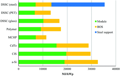 | ||
| Fig. 3 Cumulative energy demand for the production of a virtual 3 kW h solar harvesting rooftop photovoltaic installation for various thin-film technologies. Reproduced with permission from Elsevier.7 | ||
Despite this life-cycle analysis for a roof-top installation to compare these thin-film technologies, it must be kept in mind that the potential application for these thin-film technologies can be quite different and not all are best suited for roofing since their strengths lie elsewhere. Dye-sensitised devices, for example, are one of the few technologies that are transparent and colourful which make them a unique and feasible candidate for integrated photovoltaic architectural elements, such as windows.8 Even in a standard glass dye-sensitised device, FTO glass is the main factor that contributes to the energy production cost and life cycle impact of the DSSCs. Despite the fact that glass can be easily and efficiently recycled, it would be great if the additional costs for support are handled by the support of the window. Ideally, the environmental impact of such devices could be even lower since a large impact of the module comes from the FTO glass substrate (see Fig. 4), which could have double function for the glass of the window, making the whole system ‘greener’. The same is true for dye-sensitised photoelectrochemical cells (DS-PEC) for solar fuel production, which only need one substrate onto which the semiconductor is applied, making them an attractive candidate for solar fuel production. While no life-cycle analysis has been performed for DS-PEC, a more general life cycle assessment for large-scale hydrogen production via photoelectrochemical water splitting has been reported.9 Due to their very similar compounds, an additional perk for dye-sensitised systems is that discoveries made in the area of dye-sensitised solar cells can readily be transferred to DS-PCE for hydrogen production and vice versa. Furthermore, in contrast to most other technologies, dye-sensitised light harvesting systems can work under diffuse and dim-light conditions, since they do not depend as much on the angle of light incidence.10 The latter makes them – together with perovskite solar cells – also ideal for application of portable electronics and the Internet of Things (IOT).11 Despite the rise of perovskite solar cells over the last few years and their impressive increase in performance, the attractiveness of dye-sensitised solar harvesting systems has not faded due to their transparency and wide colour variety, as well as their fabrication from earth abundant materials at relatively low temperatures.
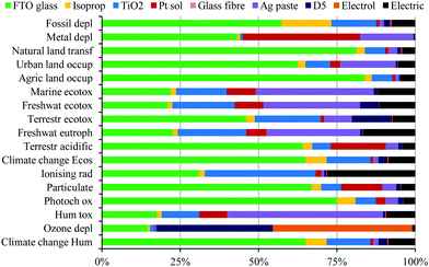 | ||
| Fig. 4 Characterisation diagram of the environmental profile for the different device components in the manufacturing process of a virtual module with the organic D5 dye and I−/I3− liquid electrolyte. Reproduced with permission from Elsevier.7 | ||
2.2 Dye-sensitised solar harvesting devices
In comparison to the previously mentioned solar harvesting devices, the advantage of dye-sensitised systems lies in their versatility and tunability which is harder to achieve with other renewable energy devices. The spectral response and dye energy positions with regard to the chosen semiconductor can be easily adjusted by changing the dye structure, along with the colour of the device. Their variety of substrates as well as their ability to work under varying lighting conditions and shaded, diffuse light make them attractive for low density and indoor applications. In addition to their transparency, this gives dye-sensitised devices unique areas of application and they can be considered a green technology due to their aforementioned low energy manufacturing demand and fabrication from abundant resources.Despite their promising future, dye-sensitised solar harvesting devices are lagging behind due to their relatively low efficiency which has not increased as drastically over the last decade as it has for other technologies. Despite the fact that the most efficient dye-sensitised solar cell is currently an n-type dye-sensitised device based on a liquid electrolyte (14% reported record efficiency12), devices with a solid-state electrolyte have several advantages, such as the prevention of leakage, evaporation or dye desorption, and, maybe most importantly, a much cheaper device fabrication route for large-scale applications, printing, as well as opening the possibility of leakage free flexible devices.13–15 Unfortunately, these advantages usually come with a lower overall performance due to a faster charge recombination.16,17
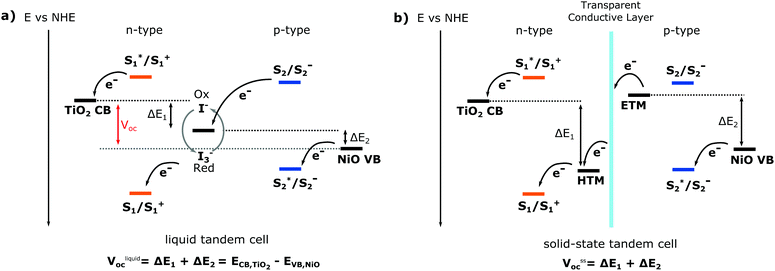
The basic working principle of dye-sensitised solar energy conversion devices is either (i) for n-type: the injection of an electron from the excited dye into the conduction band of the sensitised semiconductor and consecutive oxidation of the electrolyte (or catalyst/water for solar fuel devices) and (ii) for p-type: the injection of a hole from the excited dye into the valence band of the sensitised semiconductor, as illustrated in Fig. 5. For a solar cell, the oxidised or reduced dye regenerated by the redox mediator (electrolyte), which then is regenerated through the counter electrode. Through this process, the electrons and holes move in opposite directions, facilitating charge separation and generating a photocurrent. The magnitude of the photocurrent depends on the number of dye molecules that absorb light and the dye utilisation factor, or more generally, how much absorbed light is converted into a current. The open circuit voltage (Voc) of a single cell is the potential difference between the redox mediator and the Fermi level of the semiconductor (Fig. 5). For a DS-PEC water splitting device, a catalyst is typically co-immobilised on the semiconductor surface that facilitates either oxygen evolution (for n-type) or hydrogen evolution (for p-type).
One way to immensely boost the theoretical efficiency of dye-sensitised solar harvesting devices is to combine the n-type dye sensitised device (based on a n-type semiconductor) with a p-type dye-sensitised device (based on a p-type semiconductor) into a tandem dye-sensitised solar harvesting device. This potential advancement in dye-sensitised solar harvesting devices is the reason why p-type dye-sensitised devices have gained increasingly more attention despite their poor performance. Both DS-PEC and DSSCs would greatly benefit from a tandem system; a tandem DS-PEC would be able to achieve full water splitting without a traditional counter electrode (usually Pt).
For dye-sensitised solar cells, the ultimate goal would be to develop tandem solid state DSC devices (t-ssDSC) by exchanging the liquid electrolyte with a solid state charge transport material. Such a tandem device would no longer share the same redox mediator and electrolyte, instead each photoelectrode would have its own charge-transport material to replace the electrolyte. By connecting the photoelectrodes with a transparent and conductive layer to perform inner charge transfer, such a tandem solid state dye-sensitised solar cell, as illustrated in Fig. 5, would be able to reach a much higher Voc and no longer be limited by the potential difference of the two semiconductors, leading to a proposed efficiency of up to 18% with a potential of 2 V based on complementary light absorption of the dyes on both photoelectrodes.18
Due to the aforementioned potential of tandem devices, developing p-type dye-sensitised solar harvesting devices is crucial to emerge into a new era for dye-sensitised systems, boosting the efficiency considerably while still remaining a low-cost photoconversion device with all the previously discussed advantages. Currently, the fabrication of a tandem device with high efficiency is still hindered by the poor performance of p-type devices since a balanced photoanode and photoelectrode (p-type and n-type half cell) is required for such a device. The smallest photocurrent in the system will determine the overall photocurrent of the cell if connected in series. This means that the device can only be as efficient as the weaker half cell, which is problematic since the reported p-type efficiencies are significantly lower than their n-type counterparts.19,20 Due to this immense application potential of p-type dye-sensitised solar harvesting devices, increasing their efficiency is crucial for the advancement for dye-sensitised solar cells and solar fuel devices in general.
While this perspective focuses on the semiconductor materials, it should be noted that there are multiple ways to improve the efficiency, and focusing on the individual components as well as their interaction is significant to move forward. Advances in the dyes,21–26 electrolytes19,21,27–29 or in general17,21 can be found in the literature.
3 Semiconductor challenges for p-type dye-sensitised photocathodes
While the selection of earth abundant and ‘green’ elements with a low environmental impact is important for the large-scale feasibility, this does not guarantee that the final material or device will be cheap and green. The total impact of the cell is the sum of the various steps that need to be considered for the eco-efficiency of the final system: (i) the processing of raw materials for the chemical composition, (ii) the synthesis process for all components, (iii) the implementation into the system and (iv) the disassembly and recycling of all materials.303.1 Chemical composition
The ideal p-type semiconductor metal oxide for photocathodes used in dye-sensitised solar cells would be transparent to ensure maximal absorption of light by the dye, exhibit large hole mobility and stability, as well as a deep valence band position to increase the possible open circuit voltage (Voc). For photoelectrochemical cells for solar fuel production, the semiconductor can be transparent and work similarly to a traditional dye-sensitised solar cell where all light is absorbed by the dye, and may also be a narrow band gap semiconductor that absorbs visible light. Upon illumination, the semiconductor can then transfer electrons into the co-catalyst on the surface with the dye acting as an additional light harvesting pathway. While not realised yet and unconventional in the traditional definition of dye-sensitised solar cells, narrow band gap semiconductors could also be utilised that inject electrons into the dye or electrolyte/solid-state electron transporting material, or in other words, a p/n-junction with the dye as the additional light harvester.However, regardless of the final utilisation, good p-type metal oxide semiconductors are scarce due to fundamental reasons: for most p-type metal oxide semiconductors, the valence band is dominated by localised oxygen 2p orbitals, which leads to a high probability for the hole to be localised around the oxygen atoms and ultimately to poor hole mobility due to the need to overcome a large energy barrier to migrate.31–33
The search for efficient dye-sensitised photocathodes over the years has led to the exploration of other p-type semiconductor materials besides NiO, which is the most common semiconductor for p-type dye-sensitised photocathodes, both in solar cells and photoelectrochemical cells. Due to its large band gap of 3.6–4.0 eV,38 NiO exhibits good transparency for thin films, despite the underlying brown colour due to Ni3+ ions that are present as a result of Ni2+ vacancies that form during sintering.21 In an investigation of a range of different mesoporous NiO electrodes prepared by different research groups, Gibson et al.39 could show that the performance of NiO depends on not only the crystallite size and film thickness but also on sintering temperature, all of which influence the crystallinity and surface states. Furthermore, Hammarström et al.40 found out that these surface states are involved in hole trapping and act as tunnelling sites on a sub-ps timescale which lead to rapid recombination with the redox mediator. The issues mentioned above hint at the various challenges that are connected to make efficient photocathodes with this earth abundant material. Despite NiO being the most common p-type semiconductor for dye-sensitised photocathodes, NiO exhibits a high density of traps and a low hole mobility, and therefore small diffusion length for holes, leading to fast charge recombination.41
Among those studied are the earth abundant binary copper oxides, CuO and Cu2O. The former has a comparably small optical band gap (see Fig. 6), thus making it less transparent, but has gathered attention due to its ease of fabrication, higher conductivity and good stability. In contrast, Cu2O has a wider band gap but suffers from stability issues.42 Cuprous and cupric oxides as well as their heterojunctions have been used repeatedly for photocatalytic H2 production with a high conversion efficiency,43,44 and n-type dye sensitised CuO/TiO2 cells have been employed for hydrogen generation.45 However no p-type dye-sensitised PEC devices have yet been reported to our knowledge. Nonetheless, Lu et al.46 have managed to prepare Cu2O films for p-type dye-sensitised solar cells with a reasonable voltage of 710 mV and a photon-conversion efficiency (PCE) of 0.42% with a liquid electrolyte. One of the most transparent metal oxides is n-type degenerate tin-doped indium oxide (ITO) that has shown to be able to both accept and donate electrons from and to the photosensitiser if dye-coated.47,48 Unfortunately, indium is one of the critical elements in the periodic table (Fig. 2), otherwise its low sheet resistance and relatively low temperature preparation (see Fig. 7) make this an attractive metal oxide. Huang et al.47 have intensely studied ITO with p-type dyes for p-DSCs and Bach et al.49 were able to fabricate a liquid p-DSC based on ITO films with a PCE of up to 2%, which is close to that of the best reported analogous NiO devices. Additionally, the group of Meyer et al. was able to fabricate a photocathode with ITO with a “donor–dye–catalyst” assembly for water reduction with an increased hydrogen evolution efficiency compared to simple dye–catalyst structures on p-type metal oxides.50
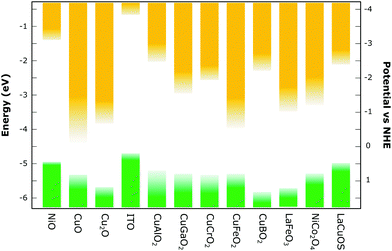 | ||
| Fig. 6 Selection of reported parameters for various p-type metal-oxide semiconductors which have also been utilised in p-type dye-sensitised solar cells. Exact values can differ depending on synthesis methods and testing conditions used. This is indicated by the ‘fading’ of the band positions – a larger fade-out represents a larger difference of the reported band positions. A graph was made with data from the literature.21,34–37 | ||
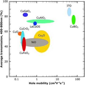 | ||
| Fig. 7 Comparison of the several p-type metal oxides from the literature showing transmission over the visible range and hole mobility. The larger circles indicate a larger variation of the reported values for the materials. The figure was obtained with data from the literature.21,52–56 | ||
Another group of semiconductor materials that have attracted much attention recently are ternary oxides, especially copper oxides (CuMO2 with M = B, Al, Ga, Cr, Fe…). Not only do these delafossite Cu(I) ternary oxides consist of earth abundant elements but also additionally benefit from favourable cation size and the mixing of the d-states of the M(III) ions with the oxygen p orbitals and reduce the hole localisation through orbital hybridisation in contrast to most other metal oxides that suffer from low hole mobility due to localised oxygen 2p orbitals.51 The typical delafossite structure has two polytypes that depend on the stacking of alternating layers of MO6 octahedra and two-dimensional packed Cu+ ions. The polytype with rhombohedral symmetry is referred to as “3R” (space group R3m) and the “2H” polytype with an alternating stacking sequence (space group P63/mmc).
Due to its large band gap and thus high transparency, CuAlO2 has been intensely studied for solar harvesting devices in the past decade. While CuAlO2 has been shown to work for dye-sensitised solar cells, the PCE of the devices is comparably small.57–59 The low performance is largely a result of the synthesis, where for example a large particle size leads to low dye loading and consequently low photocurrent. However, even with smaller CuAlO2 nanoparticles, reaching higher efficiencies is still challenging. More recently, a study by Ursu et al.60 that investigated the effect of polymorphism showed that the presence of the 2H-CuAlO2 polytype in small concentration increased the efficiency compared to the pure 3R polytype. Photocatalytic hydrogen evolution has been achieved over CuAlO2,61,62 but has not yet been realised with the addition of a dye.
Other popular delafossite Cu(I) ternary oxides are CuGaO2 and CuCrO2 due to their large band gap. Comparably, the band gap of the iron (making this material very earth abundant) analogue CuFeO2 is small, resulting in a strongly absorbing semiconductor which decreases the amount of light absorbed by the dye, consequently decreasing the photocurrent (see Fig. 6).73,74 Zhu et al.63 have reported a p-DSC with CuFeO2 that was able to reach a significant photovoltage but only reached a photocurrent of 71 μA cm−2. Despite not reaching record efficiencies, liquid p-DSCs fabricated with CuGaO2,66 as well as CuCrO264,75 have been reported to reach comparable efficiency values to analogue DSCs based on NiO under similar conditions which shows the potential of these materials. Solar hydrogen production has been realised for non-dye sensitised CuGaO276–78 and CuCrO279,80 as well as Ru(II)–Re(I) supramolecular photocatalysts sensitised on the CuGaO2 surface.67 For CuCrO2, Reisner et al.65,81 have successfully prepared photocathodes for water splitting with coimmobilised p-type organic dyes and a phosphonated molecular Ni catalyst. Similar to the other delafossite Cu(I) oxides, the reported dye-photocathodes of CuBO2 for solar cells showed a smaller photocurrent due to a low specific surface area but showed promise with a larger photovoltage than the NiO comparable device;68 however photocathodes for water splitting have not been reported. It should be noted that investigations on charge-transfer processes with different driving forces (that arise with alternative metal oxides) could show that insufficient driving forces could hinder hole injection from the dye into the semiconductor.21 This underlines the importance of tailoring the sensitisers to the individual semiconductor metal oxides and their properties, which could pave the way for more efficient photocathodes.
Unlike most of the aforementioned p-type metal oxide semiconductors, perovskite lanthanum iron oxide (LaFeO3) has not been employed for solar cells but only in dye-sensitised photoelectrochemical cells for H2 generation.69 It has a suitable band gap in the range of 2.1 to 2.6 eV, and absorbs visible light and exhibits high stability under illumination in aqueous solutions, making it interesting for solar hydrogen production.37,82 Sun et al.69 utilised the molecular dye and phosphonated molecular Ni as the hydrogen production catalyst (NiP) and could show that the dye-sensitised photocathode (NiP + dye)@LaFeO3 outperformed the non-sensitised NiP@LaFeO3 photocathode due to light absorption by both the molecular dye and LaFeO3.
An additional type of p-type semiconductor is the group of oxysulfides, which replace oxygen with a chalcogen in order to overcome the hindrance of localised oxygen p-orbitals that decrease charge mobility.83 One representative of this group is LaCuOS, which has a higher conductivity and transparency than NiO and can be successfully synthesised by a low temperature solvothermal method.84 Jobic et al.70 demonstrated the successful implementation of LaOCuS as a photocathode in p-DSSCs, however showed several synthetic challenges and low surface area as well as poor binding affinity for the dye, which is why ternary oxides might currently be considered a more promising approach.
Another material class worth mentioning are the spinel structures, AB2O4 (for example NiCo2O4) falls into this class of p-type semiconductors, which has a reported higher conductivity than NiO.85 The fabrication of a p-DSC with NiCo2O4 nanowire–nanosheet arrays sensitised with a ruthenium dye yielded relevant photo-conversion efficiency (PCE = 0.78%), which shows the potential of spinel semiconductors.71,86 While NiCo2O4 has been utilised for solar hydrogen production,87,88 DS-PEC cells have not been investigated yet. The second spinel that has been tested for dye-sensitised systems is CuFe2O4, which was used by Li et al.72 for photoelectrochemical cells and was able to reach a decent efficiency.
The summarised standard solar cell and solar fuel data for the current metal oxide semiconductor materials beyond NiO in Table 1 show that a lot of materials are still left unexplored for dye-sensitised systems as well as the low photocurrent for all p-type semiconductors. This can be related to the low hole conductivity in the discussed materials as shown in Fig. 7 as well as a low surface area for some of the reported materials. The photocurrent is especially meaningful for the successful development of tandem dye-sensitised solar harvesting devices and finding strategies to improve the photocurrent will be the main challenge in reaching this goal. For materials with a lower charge conductivity, the electrode design and structure will play an important role and are briefly discussed in the following sections.
| Dye | Electr./cat. | V oc (mV) | J (mA cm−2) | η PCE/ηF | ||
|---|---|---|---|---|---|---|
| Cu2O | DSC | C343 | I3−/I− | 710 | 1.30 | 0.4246 |
| PEC | ||||||
| ITO | DSC | Ru-8T | Fe2+/3+ | 712 | 5.65 | 1.9649 |
| PEC | RuP2-DA | NiP | 0.06 | 5350 | ||
| CuAlO2 | DSC | Ru-6T | I3−/I− | 333 | 0.30 | 0.0458 |
| PEC | ||||||
| CuFeO2 | DSC | C343 | I3−/I− | 365 | 0.07 | 0.0163 |
| PEC | ||||||
| CuCrO2 | DSC | PMI-6T-NDI | Co2+/3+ | 734 | 1.23 | 0.4864 |
| PEC | PMI-P | NiP | 0.03 | 4165 | ||
| CuGaO2 | DSC | PMI-NDI | Co2+/3+ | 305 | 0.42 | 0.0566 |
| PEC | RuRe | RuRe | 0.02 | 7267 | ||
| CuBO2 | DSC | DPP-NDI | Co2+/3+ | 453 | 0.02 | 0.00168 |
| PEC | ||||||
| LaFeO3 | DSC | |||||
| PEC | P1* | NiP | 0.02 | 4569 | ||
| LaOCuS | DSC | PMI-NDI | Co2+/3+ | 150 | 0.04 | 0.00270 |
| PEC | ||||||
| NiCo2O4 | DSC | N719 | I3−/I− | 189 | 8.35 | 0.7971 |
| PEC | ||||||
| CuFe2O4 | DSC | |||||
| PEC | MnTPP | — | 0.01 | 5372 |
Other materials worth mentioning due to their elemental abundance and have not been utilised for dye-sensitised devices but have been reported for water splitting are CuNbO389,90 with a band gap of 2 eV that has been reported for hydrogen evolution and other spinel type p-type semiconductors such as CuAl2O491 and CuMn2O4 that have been less common for photocatalysis.92
In addition to p-type semiconductor materials currently under development, it should be noted that computational studies can aid in finding and developing novel conductive p-type metal oxides with desired properties. For example, K. Yim et al.33 conducted a high-throughput screening for binary and ternary oxides to identify promising p-type transparent metal oxides.
Generally, while all of these materials have not yet exceeded NiO based photocathode efficiencies, it is important to keep in mind that NiO has been studied for a much longer time for dye sensitisation and its aspects (e.g. surface states and recombination pathways) are still not fully understood in dye-sensitised systems. Nonetheless, it can be concluded that alternative p-type semiconductor materials beyond NiO are promising but need further optimisation for dye-sensitised photocathode application, as well as further investigation of the underlying charge transport processes is needed.
As previously mentioned, Cu2O is considered an attractive p-type semiconductor for dye-sensitised photocathodes both due to the deeper valence band and higher conductivity than NiO, but its instability limits the conversion efficiency of such devices and makes it unsuitable for water splitting. The idea behind the Cu2O@CuO core–shell structure was to overcome the chemical instability of Cu2O and utilise CuO as a passivating layer which has been proven to be successful.94 This thin outer layer (5 nm thickness) was also shown to facilitate the transfer of holes from CuO to Cu2O to increase the injection efficiency of the excited dye and indicates the potential of such core–shell systems for photocathodes.
For the NiO–dye–TiO2 core–shell structure, our motivation was to design a “well-oriented” structure (see Fig. 8) to facilitate injection efficiencies.95 The donor and acceptor of the designed dye should be close to their respective semiconductors, i.e. the electron donor part of the dye close to p-type NiO and the electron acceptor part close to n-type TiO2 to get fast and efficient hole and electron injection from the dye upon light illumination. This architecture led to efficient and ultrafast hole injection (>98%, ≤200 fs) as well as unprecedentedly fast dye regeneration (70–93%, ≤500 fs) and the recombination in such a core–shell NiO–dye–TiO2 structure was found to be much slower than that of the conventional dye sensitised NiO film. An additional Al2O3 inner barrier layer between NiO and TiO2 was shown to suppress charge recombination and prolong charge lifetime in the dye-sensitised film.96 Further studies by our group97 suggested that the low photocurrent is mainly due to the low utilisation fraction of the dyes of <5%, meaning that most of the dyes do not contribute to photocurrent in this system. The reason for this is that the solid electrolyte, or rather TiO2 in this case, is not electronically well connected and most of the injected electrons are trapped in unconnected electron conductors that do not contribute to the photocurrent. A unity dye utilisation factor for the same devices would improve the photoconversion efficiency significantly (up to 4%), which suggests that improving the dye utilisation is a key challenge for unlocking efficient solid-state p-type DSCs.
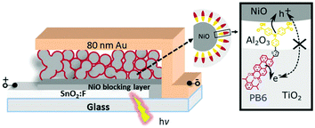 | ||
| Fig. 8 The configuration and working principle of the p-type dye sensitised NiO–dye–TiO2 core–shell solar cell, NiO–PB6–Al2O3–TiO2, with Al2O3 as an inner barrier layer and donor–π–acceptor dye PB6 as a photosensitiser. Taken from ref. 96. | ||
3.2 Synthesis and film deposition
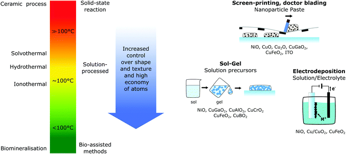
Since the energy demand of the synthesis process can greatly affect the eco-efficiency, as previously discussed for crystalline-Si solar cells, replacing high temperature synthesis methods with low temperature processes is crucial to further decrease the cumulative energy demand for the upcoming solar harvesting devices. Lowering the synthesis temperature of photocathode materials has several benefits, which are illustrated in Fig. 9. Not only do low temperature methods save energy, but shifting from high temperature synthesis routes, which are typical for solid-state reactions, towards solution based methods (hydro-, solvo- and ionothermal) or even lower temperature bio-assisted methods, increases the control of shape, size and purity of the materials.30Currently, most p-type semiconductor materials require relatively high temperature synthesis routes, typically with temperatures between 300 and 900 °C52,99 which underlines the need to develop new low-temperature synthesis methods for this type of material. Along with the temperature, the film deposition technique and growth or metal oxide thin films is the most significant factor that determines the structural, optical and electrical properties.32 Slight variations in the parameters even for the same technique can result in different properties, as shown in the previously mentioned investigation of mesoporous NiO electrodes prepared by different research groups.39
While there is a broad variety of synthesis methods for p-type transparent semiconductors,32,100 electrodes for dye-sensitised solar energy conversion require mesoporous semiconductor thin films with a high surface area (and a minimal number of grain boundaries for solar cells) to accommodate a maximal number of dye molecules (or active surface sites for (photo)catalysis) and thus, there are fewer reported deposition methods. Despite there still being a multitude of methods, the main methods for p-type dye-sensitised photocathode preparation can be narrowed down to screen printing,39,63,101 solution processed routes (which include sol–gel,39,101,102 inkjet printing21,103 and spray pyrolysis37) or electrodepostion.62,104 All of these methods are capable of large scale deposition of uniform thin films compatible with flexible substrates, such as conductive PET.105
One of the two most common deposition methods is based on a paste of premade nanoparticles (typical size 15–60 nm39,101,106) of the desired semiconductor in an ethylcellulose solution, which is transferred onto the substrate through doctor blading or screen-printing, where the paste is pushed through a mesh, before a necessary calcination step (typically 200–500 °C).39,101 Here, the fabrication of the initial nanoparticles, the preparation of the paste and the calcination temperature greatly influence the semiconductor film properties, making it hard to control fully and reproducibility across batches can be hard. However, due to its ease of fabrication and large-scale applicability, screen-printing has been reported for various p-type mesoporous semiconductors for dye-sensitised applications for NiO,39 CuO, Cu2O,107 CuGaO2,66 CuFeO2,63 CuCrO2,75 and ITO. Despite the ease of application and fabrication, this method requires two heating steps, for the nanoparticle synthesis and the calcination step, and is therefore not very energy efficient. The other common deposition method, sol–gel, which is part of the multitude of solution processed fabrication routes, only required one heating step, making this method more energy efficient. Typical precursors used are metal alkoxides in a colloidal solution (sol) that are transformed into a network (gel), most often with the help of polymers. Subsequent annealing at 300–500 °C yields a mesoporous film. This process is particularly common for most ternary oxides68,74,102,108 as well as NiO.39,109–111
Whereas electrodeposition is very common for photoelectrodes for water splitting without a dye for a few of the previously mentioned semiconductors,62,104,112 this method has not been applied to dye-sensitised photocathodes. Only for NiO104,113 and Cu/Cu2O,114 dye-sensitised systems have been reported. While electrodeposition is generally easy to control in terms of film thickness, coverage and porosity can be a challenge for this method and post-treatment is typically required; however Sonavane et al.115 have reported the electrodeposition of NiO films without necessary heat post-treatment.
With very few exceptions, all of the reported fabrication methods need an annealing or post-treatment heating step that is required to achieve crystalline semiconductor particles, and moving towards even lower synthesis routes shown in Fig. 9 due to the aforementioned advantages is desirable. For NiO synthesis, hydrothermal and solvothermal methods have been investigated that use water or alcohols, respectively, as solvent that is heated typically to 180–220 °C.116 Knowles et al.117 recently reported a novel synthesis route for phase-pure colloidal NiO nanocrystals through direct solvothermal synthesis. This also eliminated the need for commonly used postsynthetic modification steps, such as oxidation or calcination and illustrates the importance of investigating novel synthesis approaches to increase synthesis control and save energy.
4 Conclusions
Dye-sensitised solar harvesting devices are largely based on earth abundant materials, which make them a viable candidate for sustainable solar energy conversion. In order to overcome current limitations in device performance, p-type dye-sensitised solar harvesting devices are necessary to make tandem cells. However, achieving a transparent and hole conductive p-type semiconductor film for dye-sensitisation is currently one of the biggest challenges. Nonetheless, a multitude of earth abundant metal oxides have been investigated that show promise but also hurdles of p-type semiconductors that need to be overcome to reach the market stage.In order to reach the goal of synthesising a p-type dye-sensitised system that can keep up with the n-type counterpart, the focus will be mainly on improving the photocurrent, which is greatly lagging behind. This can be reached through a rational electrode design as well as developing organic dyes that are tailored to the individual needs of the chosen p-type semiconductor. Potential breakthroughs are likely to come from the development of new dyes as well as semiconductor materials beyond NiO, which is currently the standard p-type semiconductor but has inherent drawbacks due to its trap states that are promoting charge recombination and insufficient charge mobility. The development of semiconductors as well as finding a suitable synthesis and fabrication method will most likely be a key component in reaching the goal of efficient photocathodes.
Today, concerns regarding the sustainability of solar harvesting devices are steadily increasing due to the necessary large scale of devices that need to be employed over the next decade to address the ever increasing energy demand. While life-cycle assessment of systems already on the market is becoming more popular, newer technologies still in the research state are less investigated. However, even for emerging technologies, the sustainability and fabrication costs are considered equally important as the pure efficiency of the devices. While our society is becoming more aware of the importance of sustainability and undoubtedly large advances have been achieved, the question remains whether solar harvesting devices can emerge from the research stage to large scale and relatively low cost fabrication quick enough to transition fully into CO2-free electricity and fuel production in the next two decades while meeting the increasing energy demand.
Conflicts of interest
There are no conflicts to declare.Acknowledgements
The authors acknowledge Uppsala University and the Swedish Energy Agency (49278-1) for financial support.Notes and references
- N. S. Lewis, MRS Bull., 2007, 808–820 CrossRef.
- IEA, World Energy Outlook 2019, OECD, 2019.
- P. Breeze, Power Generation Technologies, Elsevier, 2019 Search PubMed.
- M. Tao, SpringerBriefs in Applied Sciences and Technology, Springer Verlag, 2014, pp. 9–20 Search PubMed.
- C. S. Tao, J. Jiang and M. Tao, Sol. Energy Mater. Sol. Cells, 2011, 95, 3176–3180 CrossRef CAS.
- T. E. Graedel, E. M. Harper, N. T. Nassar, P. Nuss, B. K. Reck and B. L. Turner, Proc. Natl. Acad. Sci. U. S. A., 2015, 112, 4257–4262 CrossRef CAS.
- M. L. Parisi, S. Maranghi and R. Basosi, Renewable Sustainable Energy Rev., 2014, 39, 124–138 CrossRef CAS.
- J. W. Lee, J. Park and H.-J. Jung, Energy Build., 2014, 81, 38–47 CrossRef.
- R. Sathre, C. D. Scown, W. R. Morrow, J. C. Stevens, I. D. Sharp, J. W. Ager, K. Walczak, F. A. Houle and J. B. Greenblatt, Energy Environ. Sci., 2014, 7, 3264–3278 RSC.
- S. S. Y. Juang, P. Y. Lin, Y. C. Lin, Y. S. Chen, P. S. Shen, Y. L. Guo, Y. C. Wu and P. Chen, Front. Chem., 2019, 7, 209, DOI:10.3389/fchem.2019.00209.
- S. Yun, Y. Qin, A. R. Uhl, N. Vlachopoulos, M. Yin, D. Li, X. Han and A. Hagfeldt, Energy Environ. Sci., 2018, 11, 476–526 RSC.
- K. Kakiage, Y. Aoyama, T. Yano, K. Oya, J.-I. Fujisawa and M. Hanaya, Chem. Commun., 2015, 51, 15894–15897 RSC.
- G. Li, L. Sheng, T. Li, J. Hu, P. Li and K. Wang, Sol. Energy, 2019, 177, 80–98 CrossRef CAS.
- D. Wei, H. E. Unalan, D. Han, Q. Zhang, L. Niu, G. Amaratunga and T. Ryhanen, Nanotechnology, 2008, 19, 424006 CrossRef PubMed.
- Z. Xue, C. Jiang, L. Wang, W. Liu and B. Liu, J. Phys. Chem. C, 2014, 118, 16352–16357 CrossRef CAS.
- J. Zhang, M. Freitag, A. Hagfeldt and G. Boschloo, Springer, Singapore, 2018, pp. 151–185 Search PubMed.
- G. Boschloo, Front. Chem., 2019, 7, 77 CrossRef CAS PubMed.
- H. Tian, Sustainable Energy Fuels, 2019, 3, 888–898 RSC.
- I. R. Perera, T. Daeneke, S. Makuta, Z. Yu, Y. Tachibana, A. Mishra, P. Bäuerle, C. A. Ohlin, U. Bach and L. Spiccia, Angew. Chem., Int. Ed., 2015, 54, 3758–3762 CrossRef CAS PubMed.
- A. Carella, F. Borbone and R. Centore, Front. Chem., 2018, 6, 481 CrossRef CAS PubMed.
- E. Benazzi, J. Mallows, G. H. Summers, F. A. Black and E. A. Gibson, J. Mater. Chem. C, 2019, 7, 10409–10445 RSC.
- T. T. T. Pham, S. K. Saha, D. Provost, Y. Farré, M. Raissi, Y. Pellegrin, E. Blart, S. Vedraine, B. Ratier, D. Aldakov, F. Odobel and J. Bouclé, J. Mater. Chem. C, 2017, 121, 129–139 CAS.
- M. Bonomo, S. Sheehan, D. P. Dowling, L. Gontrani and D. Dini, ChemistrySelect, 2018, 3, 6729–6736 CrossRef CAS.
- K. A. Click, D. R. Beauchamp, B. R. Garrett, Z. Huang, C. M. Hadad and Y. Wu, Phys. Chem. Chem. Phys., 2014, 16, 26103–26111 RSC.
- F. Wu, J. Liu, X. Li, Q. Song, M. Wang, C. Zhong and L. Zhu, Eur. J. Org. Chem., 2015, 6850–6857 CrossRef CAS.
- B. Xu, S. Wrede, A. Curtze, L. Tian, P. B. Pati, L. Kloo, Y. Wu and H. Tian, ChemSusChem, 2019, 12, 3243–3248 CrossRef CAS PubMed.
- V. Nikolaou, A. Charisiadis, G. Charalambidis, A. G. Coutsolelos and F. Odobel, J. Mater. Chem. A, 2017, 5, 21077–21113 RSC.
- E. A. Gibson, A. L. Smeigh, L. Le Pleux, L. Hammarström, F. Odobel, G. Boschloo and A. Hagfeldt, J. Phys. Chem. C, 2011, 115, 9772–9779 CrossRef CAS.
- H. Iftikhar, G. G. Sonai, S. G. Hashmi, A. F. Nogueira and P. D. Lund, Materials, 2019, 12, 1998 CrossRef CAS PubMed.
- D. Larcher and J. M. Tarascon, Nat. Chem., 2015, 7, 19–29 CrossRef CAS PubMed.
- H. Kawazoe, H. Yanagi, K. Ueda and H. Hosono, MRS Bull., 2000, 25, 28–36 CrossRef CAS.
- A. Banerjee and K. Chattopadhyay, Progress in Crystal Growth and Characterization of Materials, 2005, vol. 50, pp. 52–105 Search PubMed.
- K. Yim, Y. Youn, M. Lee, D. Yoo, J. Lee, S. H. Cho and S. Han, npj Comput. Mater., 2018, 4, 17, DOI:10.1038/s41524-018-0073-z.
- K. Rajeshwar, M. K. Hossain, R. T. Macaluso, C. Janáky, A. Varga and P. J. Kulesza, J. Electrochem. Soc., 2018, 165, H3192–H3206 CrossRef CAS.
- E. Schiavo, C. Latouche, V. Barone, O. Crescenzi, A. B. Muñoz-García and M. Pavone, Phys. Chem. Chem. Phys., 2018, 20, 14082–14089 RSC.
- B. A. Williamson, J. Buckeridge, N. P. Chadwick, S. Sathasivam, C. J. Carmalt, I. P. Parkin and D. O. Scanlon, Chem. Mater., 2019, 31, 2577–2589 CrossRef CAS PubMed.
- G. S. Pawar and A. A. Tahir, Sci. Rep., 2018, 8, 1–9 CrossRef CAS PubMed.
- E. L. Miller, J. Electrochem. Soc., 1997, 144, 1995 CrossRef CAS.
- C. J. Wood, G. H. Summers, C. A. Clark, N. Kaeffer, M. Braeutigam, L. R. Carbone, L. D'Amario, K. Fan, Y. Farré, S. Narbey, F. Oswald, L. A. Stevens, C. D. J. Parmenter, M. W. Fay, A. La Torre, C. E. Snape, B. Dietzek, D. Dini, L. Hammarström, Y. Pellegrin, F. Odobel, L. Sun, V. Artero and E. A. Gibson, Phys. Chem. Chem. Phys., 2016, 18, 10727–10738 RSC.
- L. D'Amario, R. Jiang, U. B. Cappel, E. A. Gibson, G. Boschloo, H. Rensmo, L. Sun, L. Hammarström and H. Tian, ACS Appl. Mater. Interfaces, 2017, 9, 33470–33477 CrossRef.
- S. Mori, S. Fukuda, S. Sumikura, Y. Takeda, Y. Tamaki, E. Suzuki and T. Abe, J. Phys. Chem. C, 2008, 112, 16134–16139 CrossRef CAS.
- O. Langmar, C. R. Ganivet, A. Lennert, R. D. Costa, G. De La Torre, T. Torres and D. M. Guldi, Angew. Chem., Int. Ed., 2015, 54, 7688–7692 CrossRef CAS.
- Z. Zhang and P. Wang, J. Mater. Chem., 2012, 22, 2456–2464 RSC.
- D. Barreca, P. Fornasiero, A. Gasparotto, V. Gombac, C. Maccato, T. Montini and E. Tondello, ChemSusChem, 2009, 2, 230–233 CrossRef CAS PubMed.
- Z. Jin, X. Zhang, Y. Li, S. Li and G. Lu, Catal. Commun., 2007, 8, 1267–1273 CrossRef CAS.
- S. Du, P. Cheng, P. Sun, B. Wang, Y. Cai, F. Liu, J. Zheng and G. Lu, Chem. Res. Chin. Univ., 2014, 30, 661–665 CrossRef CAS.
- Z. Huang, M. He, M. Yu, K. Click, D. Beauchamp and Y. Wu, Angew. Chem., Int. Ed., 2015, 54, 6857–6861 CrossRef CAS.
- Y. Furmansky, H. Sasson, P. Liddell, D. Gust, N. Ashkenasy and I. Visoly-Fisher, J. Mater. Chem., 2012, 22, 20334 RSC.
- Z. Yu, I. R. Perera, T. Daeneke, S. Makuta, Y. Tachibana, J. J. Jasieniak, A. Mishra, P. Bäuerle, L. Spiccia and U. Bach, NPG Asia Mater., 2016, 8, e305 CrossRef.
- B. Shan, A. K. Das, S. Marquard, B. H. Farnum, D. Wang, R. M. Bullock and T. J. Meyer, Energy Environ. Sci., 2016, 9, 3693–3697 RSC.
- D. O. Scanlon, K. G. Godinho, B. J. Morgan and G. W. Watson, J. Chem. Phys., 2010, 132, 024707 CrossRef PubMed.
- K. Fleischer, E. Norton, D. Mullarkey, D. Caffrey and I. V. Shvets, Materials, 2017, 10, 1019 CrossRef PubMed.
- S. Zhang, H. Ye, J. Hua and H. Tian, Energy Chem., 2019, 1, 100015 CrossRef.
- M. I. Díez-García and R. Gómez, ChemSusChem, 2017, 10, 2457–2463 CrossRef PubMed.
- A. Liu, G. Liu, H. Zhu, B. Shin, E. Fortunato, R. Martins and F. Shan, Appl. Phys. Lett., 2016, 108, 233506 CrossRef.
- L. Dong, G. Zhu, H. Xu, X. Jiang, X. Zhang, Y. Zhao, D. Yan, L. Yuan and A. Yu, Materials, 2019, 16, 958 CrossRef.
- J. Bandara and J. P. Yasomanee, Semicond. Sci. Technol., 2007, 22, 20–24 CrossRef CAS.
- A. Nattestad, X. Zhang, U. Bach and Y. Cheng, J. Photonics Energy, 2011, 1, 011103 CrossRef.
- J. Ahmed, C. K. Blakely, J. Prakash, S. R. Bruno, M. Yu, Y. Wu and V. V. Poltavets, J. Alloys Compd., 2014, 591, 275–279 CrossRef CAS.
- M. Miclau, N. Miclau, R. Banica and D. Ursu, Mater. Today, 2017, 4, 6975–6981 Search PubMed.
- N. Koriche, A. Bouguelia, A. Aider and M. Trari, Int. J. Hydrogen Energy, 2005, 30, 693–699 CrossRef CAS.
- S. Y. Choi, C. D. Kim, D. S. Han and H. Park, J. Mater. Chem. A, 2017, 5, 10165–10172 RSC.
- T. Zhu, Z. Deng, X. Fang, Z. Huo, S. Wang, W. Dong, J. Shao, R. Tao, C. Song and L. Wang, J. Alloys Compd., 2016, 685, 836–840 CrossRef CAS.
- S. Powar, D. Xiong, T. Daeneke, M. T. Ma, A. Gupta, G. Lee, S. Makuta, Y. Tachibana, W. Chen, L. Spiccia, Y.-B. Cheng, G. Götz, P. Bäuerle and U. Bach, J. Mater. Chem. C, 2014, 118, 16375–16379 CAS.
- C. E. Creissen, J. Warnan, D. Antón-García, Y. Farré, F. Odobel and E. Reisner, ACS Catal., 2019, 9, 9530–9538 CrossRef CAS PubMed.
- A. Renaud, L. Cario, P. Deniard, E. Gautron, X. Rocquefelte, Y. Pellegrin, E. Blart, F. Odobel and S. Jobic, J. Mater. Chem. C, 2014, 118, 54–59 CAS.
- H. Kumagai, G. Sahara, K. Maeda, M. Higashi, R. Abe and O. Ishitani, Chem. Sci., 2017, 8, 4242–4249 RSC.
- T. Jiang, M. Bujoli-Doeuff, Y. Farré, E. Blart, Y. Pellegrin, E. Gautron, M. Boujtita, L. Cario, F. Odobel and S. Jobic, RSC Adv., 2016, 6, 1549–1553 RSC.
- F. Li, R. Xu, C. Nie, X. Wu, P. Zhang, L. Duan and L. Sun, Chem. Commun., 2019, 55, 12940–12943 RSC.
- A. Renaud, L. Cario, Y. Pellegrin, E. Blart, M. Boujtita, F. Odobel and S. Jobic, RSC Adv., 2015, 5, 60148–60151 RSC.
- Z. Shi, H. Lu, Q. Liu, K. Deng, L. Xu, R. Zou, J. Hu, Y. Bando, D. Golberg and L. Li, Energy Technol., 2014, 2, 517–521 CrossRef CAS.
- X. Li, A. Liu, D. Chu, C. Zhang, Y. Du, J. Huang and P. Yang, Catalysts, 2018, 8, 108 CrossRef.
- C. G. Read, Y. Park and K. S. Choi, J. Phys. Chem. Lett., 2012, 3, 1872–1876 CrossRef CAS PubMed.
- M. S. Prévot, N. Guijarro and K. Sivula, ChemSusChem, 2015, 8, 1359–1367 CrossRef PubMed.
- D. Xiong, Z. Xu, X. Zeng, W. Zhang, W. Chen, X. Xu, M. Wang and Y. B. Cheng, J. Mater. Chem., 2012, 22, 24760–24768 RSC.
- M. Lee, D. Kim, Y. T. Yoon and Y. I. Kim, Bull. Korean Chem. Soc., 2014, 35, 3261–3266 CrossRef CAS.
- T. Zhang, K. Zhu, M. Chen, T. Li, P. Li, Y. Cheng, Z. Zou, W. Luo and W. Huang, J. Phys. D: Appl. Phys., 2019, 52, 405501 CrossRef CAS.
- C. D. Windle, H. Kumagai, M. Higashi, R. Brisse, S. Bold, B. Jousselme, M. Chavarot-Kerlidou, K. Maeda, R. Abe, O. Ishitani and V. Artero, J. Am. Chem. Soc., 2019, 141, 9593–9602 CrossRef CAS PubMed.
- A. Varga, G. F. Samu and C. Janáky, Electrochim. Acta, 2018, 272, 22–32 CrossRef CAS.
- S. Saadi, A. Bouguelia and M. Trari, Sol. Energy, 2006, 80, 272–280 CrossRef CAS.
- C. E. Creissen, J. Warnan and E. Reisner, Chem. Sci., 2018, 9, 1439–1447 RSC.
- I. M. Nassar, S. Wu, L. Li and X. Li, ChemistrySelect, 2018, 3, 968–972 CrossRef CAS.
- H. Hiramatsu, K. Ueda, H. Ohta, M. Hirano, T. Kamiya and H. Hosono, Appl. Phys. Lett., 2003, 82, 1048–1050 CrossRef CAS.
- C. Doussier-Brochard, B. Chavillon, L. Cario and S. Jobic, Inorg. Chem., 2010, 49, 3074–3076 CrossRef CAS PubMed.
- I. T. Papadas, A. Ioakeimidis, G. S. Armatas and S. A. Choulis, Adv. Sci., 2018, 5, 1701029 CrossRef PubMed.
- Z. Shi, H. Lu, Q. Liu, F. Cao, J. Guo, K. Deng and L. Li, Nanoscale Res. Lett., 2014, 9, 608 CrossRef PubMed.
- L. An, L. Huang, P. Zhou, J. Yin, H. Liu and P. Xi, Adv. Funct. Mater., 2015, 25, 6814–6822 CrossRef CAS.
- J. Yin, P. Zhou, L. An, L. Huang, C. Shao, J. Wang, H. Liu and P. Xi, Nanoscale, 2016, 8, 1390–1400 RSC.
- U. A. Joshi, A. M. Palasyuk and P. A. Maggard, J. Mater. Chem. C, 2011, 115, 13534–13539 CAS.
- C. T. Crespo, Sol. Energy Mater. Sol. Cells, 2018, 179, 305–311 CrossRef CAS.
- G. Li, C. Gu, W. Zhu, X. Wang, X. Yuan, Z. Cui, H. Wang and Z. Gao, J. Cleaner Prod., 2018, 183, 415–423 CrossRef CAS.
- S. Saadi, A. Bouguelia and M. Trari, Renewable Energy, 2006, 31, 2245–2256 CrossRef CAS.
- M. B. Gawande, A. Goswami, T. Asefa, H. Guo, A. V. Biradar, D. L. Peng, R. Zboril and R. S. Varma, Chem. Soc. Rev., 2015, 44, 7540–7590 RSC.
- T. Jiang, M. Bujoli-Doeuff, E. Gautron, Y. Farré, L. Cario, Y. Pellegrin, M. Boujtita, F. Odobel and S. Jobic, J. Alloys Compd., 2018, 769, 605–610 CrossRef CAS.
- L. Tian, J. Föhlinger, P. B. Pati, Z. Zhang, J. Lin, W. Yang, M. Johansson, T. Kubart, J. Sun, G. Boschloo, L. Hammarström and H. Tian, Phys. Chem. Chem. Phys., 2017, 20, 36–40 RSC.
- L. Tian, J. Föhlinger, Z. Zhang, P. B. Pati, J. Lin, T. Kubart, Y. Hua, J. Sun, L. Kloo, G. Boschloo, L. Hammarström and H. Tian, Chem. Commun., 2018, 54, 3739–3742 RSC.
- L. Tian, T. Törndahl, J. Lin, P. B. Pati, Z. Zhang, T. Kubart, Y. Hao, J. Sun, G. Boschloo and H. Tian, J. Mater. Chem. C, 2019, 123, 26151–26160 CAS.
- K. Yu and J. Chen, Nanoscale Res. Lett., 2009, 4, 1–10 CrossRef CAS.
- Y. J. Jang and J. S. Lee, ChemSusChem, 2019, 12, 1835–1845 CrossRef CAS PubMed.
- A. Stadler, Materials, 2012, 5, 661–683 CrossRef PubMed.
- D. Dini, Y. Halpin, J. G. Vos and E. A. Gibson, Coord. Chem. Rev., 2015, 304-305, 179–201 CrossRef CAS.
- B. Satish and R. Srinivasan, Mater. Today, 2018, 2401–2411 CAS.
- R. Brisse, R. Faddoul, T. Bourgeteau, D. Tondelier, J. Leroy, S. Campidelli, T. Berthelot, B. Geffroy and B. Jousselme, ACS Appl. Mater. Interfaces, 2017, 9, 2369–2377 CrossRef CAS.
- S. Koussi-Daoud and T. Pauporté, Oxide-based Materials and Devices VI, 2015, p. 936425 Search PubMed.
- C. Glynn and C. O'Dwyer, Adv. Mater. Interfaces, 2017, 4, 1600610 CrossRef.
- M. Bonomo, N. Barbero, F. Matteocci, A. D. Carlo, C. Barolo and D. Dini, J. Phys. Chem. C, 2016, 120, 16340–16353 CrossRef CAS.
- D. Ursu, M. Vajda and M. Miclau, J. Alloys Compd., 2019, 802, 86–92 CrossRef CAS.
- A. Alias, M. Sakamoto, T. Kimura and K. Uesugi, Phys. Status Solidi C, 2012, 9, 198–201 CrossRef CAS.
- S. Sumikura, S. Mori, S. Shimizu, H. Usami and E. Suzuki, J. Photochem. Photobiol., A, 2008, 199, 1–7 CrossRef CAS.
- N. N. M. Zorkipli, N. H. M. Kaus and A. A. Mohamad, Procedia Chem., 2016, 19, 626–631 CrossRef CAS.
- M. Jlassi, I. Sta, M. Hajji and H. Ezzaouia, Surf. Interfaces, 2017, 6, 218–222 CrossRef CAS.
- C. G. Read, Y. Park and K. S. Choi, J. Phys. Chem. Lett., 2012, 3, 1872–1876 CrossRef CAS PubMed.
- S. Koussi-Daoud, A. Planchat, A. Renaud, Y. Pellegrin, F. Odobel and T. Pauporté, ChemElectroChem, 2017, 4, 2618–2625 CrossRef CAS.
- F. Shao, J. Sun, L. Gao, J. Luo, Y. Liu and S. Yang, Adv. Funct. Mater., 2012, 22, 3907–3913 CrossRef CAS.
- A. C. Sonavane, A. I. Inamdar, P. S. Shinde, H. P. Deshmukh, R. S. Patil and P. S. Patil, J. Alloys Compd., 2010, 489, 667–673 CrossRef CAS.
- L. Qiao and M. T. Swihart, Adv. Colloid Interface Sci., 2017, 244, 199–266 CrossRef CAS PubMed.
- D. A. Brewster, Y. Bian and K. E. Knowles, Chem. Mater., 2020, 1 Search PubMed.
| This journal is © the Owner Societies 2020 |


