
 Open Access Article
 This Open Access Article is licensed under a Creative Commons Attribution-Non Commercial 3.0 Unported Licence
Nanostructured ZnO thin films for self-cleaning applications
Mohamed Shaban *,
Mohamed Zayed and
Hany Hamdy
*,
Mohamed Zayed and
Hany Hamdy
Nanophotonics and Applications Lab, Department of Physics, Faculty of Science, Beni-Suef University, Beni-Suef 62514, Egypt. E-mail: mssfadel@yahoo.com; mssfadel@aucegypt.edu; Tel: +20 1274493440
First published on 3rd January 2017
Abstract
Controlling the properties of nanostructured zinc oxide (ZnO) is an interesting way to broaden its multifunctionality. ZnO nanostructured films were grown on glass substrates under different conditions by a simple two-step wet chemical method. A low-cost successive ionic layer adsorption and reaction (SILAR) method was used to grow ZnO seed layers at 80 °C. Then, different hierarchical based ZnO nanostructured thin films were deposited onto the ZnO seed layers by chemical bath deposition (CBD). The influence of deposition time (tD) and pH on the surface morphology, wettability behavior, structural and optical properties of the ZnO nanostructured films were systematically investigated. The structural, morphological, optical and wetting properties were studied by X-ray diffraction (XRD), field emission scanning microscopy (FE-SEM), UV-Vis spectrophotometer, and water contact angle (WCA) measurement, respectively. The surface morphology revealed a complex and orientated hierarchical based ZnO nanostructured films with diverse shapes from hexagonal nanorods to hexagonal nanoplates and even much more complex plates/rods and flower-like shapes by changing deposition time and pH of the precursor. XRD results confirm the synthesis of nanostructured ZnO of the hexagonal structure with a preferential orientation along the (002) lattice plane. The average crystallite size, D, is altered between 41.41 to 68.43 nm dependent on the morphology of the ZnO film and pH of the precursor. At pH 6.5, the films are hydrophilic for 10 h ≤ tD ≤ 6 h and hydrophobic for 6 h < tD < 10 h. The wetting properties of the films were enhanced by increasing or decreasing pH around 6.5. Morphology and thickness of the ZnO nanostructure could efficiently control the transmittance, absorbance, optical band gap, and the extinction coefficient of the films. The optical band gap is blue shifted from 2.45 to 3.62 eV@pH 6.5 as the deposition time increased from 2 to 8 h and blue shifted from 2.72 to 3.62 eV@8 h as the pH value increased from 5.5 to 6.5. The existence of stable hydrophobic zinc oxide nanostructured films at room temperature at a large-scale and with band gaps around 3.62 eV supports their use in self-cleaning and gas sensing applications.
1 Introduction
The wetting behavior of a film is a combined effect of its surface topography and microstructure, surface free energy, and the chemical composition.1,2 In general, surfaces with water contact angle Θ ≥ 90° are hydrophobic and those with contact angles Θ < 90° are hydrophilic.3 The development of semiconductor (SC) metal oxide thin films of different morphologies with self-cleaning properties is one of the key technologies for optoelectronic applications. ZnO nanostructures exhibit strong spontaneous piezoelectric polarization because of their wurtzite structure, a hexagonal lattice in which the Zn2+ ions occupy the tetrahedral sites formed by the O2− ions.4 ZnO surfaces display better photocatalytic performance in the degradation of hazard dye molecules in both basic and acidic medium.5 ZnO films have thermal diffusivity in the range of (4.35–5.03) × 10−2 cm2 s−1 and electrical resistivity varying from 10−4 to 1012 Ω cm.6 The free exciton binding energy of ZnO at room temperature (RT) can be increased from 60 meV to >100 meV in superlattices.7 These distinctive physicochemical and optoelectronic properties of the transparent ZnO semiconductor material still stimulate enormous awareness for usage in a variety of industrial and technological applications. ZnO films are suitable for monitoring of some gasses like CO and H2S and CH4.8 ZnO is considered as a next-generation light-emitting diode (LED) and room temperature (RT) polariton lasers.9–12 ZnO film can be used as front contact material for dye-sensitized solar cells12,13 because of its relatively high optical transmittance in the visible region and conductivity. Also, ZnO nanoparticles (NPs) were used in cosmetics and paints because of its ability to block the UV light.14,15ZnO surfaces are generally hydrophilic (water contact angle Θ < 90°).16 The hydrophilic and superhydrophilic surfaces are used for practical applications such as antifogging and self-cleaning.17 However, hydrophobic and superhydrophobic surfaces can be used in many areas as antifouling, anti-icing, self-cleaning, and liquid transportation. Different approaches have been used to turned the ZnO surfaces from hydrophilic to hydrophobic.18 UV illumination and long-term dark storage (or heating) are simple methods for the hydrophilic & hydrophobic transition. Also, doping and co-doping with specific elements is another way that could be used to turned the wettability of ZnO surfaces from hydrophilic to hydrophobic for some particular applications and needs. For this purpose, different elements are used as dopants or co-dopants of ZnO films such as Na, La, Pb, Mg, (Pb–Mg).5,19,20 Also, Thirumalai et al.21 reported that bentonite supported Bi2O3–ZnO possesses a significant hydrophobicity (a contact angle of 126°) which leads to its self-cleaning property. Additionally, many authors tried to control the morphology of undoped ZnO surface to obtain hydrophobic surfaces or coatings. I.e., control of the self-cleaning property depends on the geometrical structure of film surface. Especially, nanorods and nanowires ZnO array-based films almost are hydrophobic and used as self-cleaning coatings on glass.22,23 Various techniques have been utilizing to prepare hydrophobic ZnO nanostructured films for self-cleaning application such as magnetron sputtering, spray pyrolysis, thermal oxidation, reactive evaporation, vapor phase epitaxy, electrodeposition, sol–gel, solid-state reaction and, chemical deposition.23–30 ZnO nanorods3 and nanodiscs25 synthesized by a hydrothermal method as well as ZnO nanowires fabricated using thermal evaporation method,26,27 were reported. ZnO nanowires by long-pulse-width laser ablation (LPLD) was also reported.28 Similar results were reported for ZnO nanorods2 and thin films prepared by radio-frequency (RF) magnetron sputtering.31 However, there is high demand for low cost and massive production of hydrophobic ZnO nanostructured surfaces for many applications such as indoor self-cleaning.
Different techniques have been used to develop ZnO nanostructures such as magnetron sputtering,31 thermal evaporation,32 atomic layer deposition,33 vapor phase epitaxy, solid-state reaction, and hydrothermal method.34–41 But these techniques required ultra-high vacuum, costly equipment, catalysts, high operation temperatures, or the use of toxic gas compounds. Compared with the previous techniques, controlled fabrication of nanostructured ZnO films by chemical bath deposition (CBD) is smarter because of its excellent features. This is ascribed to its ability to control the morphology and orientation of ZnO by tuning the process parameters.42 Also, it is inexpensive, simple, rapid, applicable for large scale production, and working under low temperatures (<100 °C) using a variety of substrates.30 Most of the previous CBD reports mainly focused on the control of the ZnO nanostructures morphology by altering the concentration and temperature of the solution.43,44
Successive ionic layer adsorption and reaction (SILAR) has attracted particular interest for preparing the ZnO nanostructure due to its simplicity and low-cost. This is beside its capability to achieve large area coatings and ability to control the morphology of nanostructure.43,44 Based on the literature survey, there are few reports of nanostructured ZnO thin films prepared by SILAR technique. Also, most of the previously reported ZnO films by this method were hydrophilic. Additionally, chemical bath deposition (CBD) is more interest because of its excellent characteristics. The CBD can control the orientation and morphology of ZnO by tuning the fabrication parameters.45 Also, it is a rapid, simple, inexpensive, applicable for large scale production, and working under low temperatures (<100 °C) using a variety of substrates.46 Most of the previous reports with CBD mainly focused on the control of the ZnO nanomorphology by changing the temperature and concentration of the solution.47,48 In the present work, the different fabrication parameters of CBD technique will be controlled and optimized to produce hydrophobic ZnO nanostructured coatings on glass substrates coated with seed layer by SILAR technique. In addition, the influences of the deposition time and pH value on the morphological, structural, hydrophobic, and optical properties nanostructured ZnO thin films are reported.
Hydrophobic ZnO nanoarrays have been deposited by several techniques such as pulsed laser deposition,49 sintering,50 chemical spray,51 sol–gel,52 chemical bath deposition (CBD),53 a heating reflux,54 simple successive ionic layer absorption and reaction (SILAR),55 hydrothermal,56 and R.F magnetron sputtering.57
2 Experimental details
2.1. Materials
Zinc acetate dihydrate (Zn(CH3COOH)·2H2O, ADWIC, 98.5%), citric acid (Fluka, 99.5%), zinc sulphate (Zn(SO4), Alfa Aesar, 99%), ammonia (NH4OH, Alfa Aesar), sodium hydroxide (NaOH, Alfa Aeasar, 99.6%), hexamethylene tetra-ammine (C6H12N4 (HMT), ADWIC, 99%), and hydrochloric acid (HCl, Alfa Aesar, 98%) were used as received from the supplier.2.2. Deposition of ZnO nano-seeds layer
To grow well-nanostructured ZnO thin films, first, a nanostructured ZnO seed layer film was deposited on glass substrates using SILAR method. This ZnO-coated substrate is then used for growing ZnO NRs by using CBD method. It is a very simple and relatively cost-effective method for preparing films of any preferred composition under controlled conditions.Before use, the glass substrates were washed for 45 min in boiled dilute sulfuric acid (1![[thin space (1/6-em)]](https://www.rsc.org/images/entities/char_2009.gif) :10 v/v) and then thoroughly rinsed in ethanol, acetone, and deionized (DI) water subsequently. Analytical reagents of ZnSO4 were dissolved in diluted ammonia to obtain a zinc ammonium complex solution. This solution was then served as a cationic precursor. Double distilled water (DDW) kept at 80 °C was used as an anionic precursor. The SILAR growth is a four step process involving subsequent immersion of cleaned glass substrate in cationic and anionic solution along with rinsing the substrate in between in DDW kept at room temperature. In the first step, the substrate was immersed in a beaker containing Zn(SO4) and ammonia solution for 40 s, where Zn2+ with ammonia formed zinc ammonia complex ([Zn(NH3)4]2+) which adsorbed onto the glass substrate, eqn (1).
:10 v/v) and then thoroughly rinsed in ethanol, acetone, and deionized (DI) water subsequently. Analytical reagents of ZnSO4 were dissolved in diluted ammonia to obtain a zinc ammonium complex solution. This solution was then served as a cationic precursor. Double distilled water (DDW) kept at 80 °C was used as an anionic precursor. The SILAR growth is a four step process involving subsequent immersion of cleaned glass substrate in cationic and anionic solution along with rinsing the substrate in between in DDW kept at room temperature. In the first step, the substrate was immersed in a beaker containing Zn(SO4) and ammonia solution for 40 s, where Zn2+ with ammonia formed zinc ammonia complex ([Zn(NH3)4]2+) which adsorbed onto the glass substrate, eqn (1).
| ZnSO4 + 4NH3· H2O → [Zn(NH3)4]2+ + H2SO4 | (1) |
In the second step, the zinc ammonia adsorbed substrate was immersed into a beaker containing DDW for 20 s. As a result, the adsorbed zinc ammonia complex was converted into zinc hydroxide (Zn(OH)2); eqn (2).
 | (2) |
As a third step, the Zn(OH)2 coated substrate was imperiled for 60 s to ultrasonic agitation for removing loosely bonded zinc hydroxide (Zn(OH)2) molecules. Finally, the zinc hydroxide coated substrate was immersed in the DDW bath which was kept at 80 °C for 20 s to convert Zn(OH)2 to solid ZnO film, eqn (3).
| Zn(OH)2 → ZnO(s) + H2O | (3) |
The film was dried for 15 s before the repeating of the deposition cycle. The as-prepared ZnO seed layer films were subjected to annealing at 300 °C for 1 h. The ZnO seed layer films were prepared at 20 cycles.
2.3. Growth of hierarchical ZnO nanostructure thin films
The deposition of hierarchical ZnO nanostructured films onto seed layer films were carried out by using simple chemical bath deposition (CBD) method. All the chemicals were purchased from Aldrich Chemical Corporation and used without further purification. The chemical bath was prepared by mixing equimolar (0.05 M) aqueous solution of zinc acetate dihydrate Zn(CH3COOH)·2H2O and hexamethylene tetra-ammine (HMT) were dissolved in 20 ml of DI water. When these two compounds were mixed, no precipitation was observed. Finally, white precipitation was observed after continued stirring for 20 min. The pH of the reaction was controlled at 4, 5, 6, 7, and 8 by adding a 0.1 M sodium hydroxide (NaOH) or 0.1 M hydrochloric acid (HCl) solution. After successful completion of deposition condition, the temperature of the water bath was allowed to cool down to ambient temperature. Finally, the deposited films were removed from the aqueous solution and cleaned carefully with DI water and acetone for several times to remove residual salts and then dried at room temperature for further characterization.2.4. Samples characterization
X-ray diffraction (XRD, High-resolution Philips X'PertPRO MRD) was used to identify the crystallographic properties of the prepared ZnO films using Cu Kα radiation (λ = 1.5418 Å) with a step 0.02. The chemical compositional was analyzed using energy dispersive X-ray (EDX; Oxford Link ISIS 300 EDX). Morphological studies of the fabricated nanostructured films were carried out using field emission-scanning electron microscopy, FE-SEM (model: ZEISS SUPRA 55 VP and ZEISS LEO, Gemini Column). Optical spectra in the spectral range 300–1000 nm were measured using UV/VIS/NIR 3700 double beam Shimadzu spectrophotometer at RT. The surface wettability of ZnO thin films was identified by measuring the water contact angle, WCA(Θ). WCA was measured using the sessile drop method by a CAM 200 Optical Contact Angle Meter (KSV Instruments). A 5 μl droplet of deionized (DI) water was positioned on the surface of the sample by a microsyringe. The image of the droplet was captured to measure the angle that formed at the liquid/solid interface. The WCA was measured three times for each sample and the average value was calculated.3 Results and discussion
3.1. Structural studies
The XRD patterns of ZnO nanostructured films grown at various deposition time, tD, from 2 to 12 h are shown in Fig. 1. All films exhibit polycrystalline structures. All the peaks are for the hexagonal wurtzite ZnO and space group C6V = P63mc (JCPDS-89-0510).58,59 All films show a strong (0 0 2) diffraction peak at 34.40° and grow preferentially perpendicular to the substrate surface along c-axis. There are other weak peaks at 31.72°, and 36.21°, 47.45°, 56.58°, 62.89°, and 67.86° correspond to (1 0 0), (1 0 1), (1 0 2), (1 1 0), (1 0 3) and (1 1 2) orientation planes of ZnO. No additional impurity phases or metallic Zn phases are detected, which indicates the formation of pure crystalline ZnO films at the relatively lower time of 2 h and the precursors were completely transformed into ZnO phase. With the increase of deposition time till 8 h, the (0 0 2) peaks became stronger and sharper that demonstrated the better growth and crystallization of ZnO thin films. With increasing the deposition time tD ≥ 10 h, the intensity along (0 0 2) direction is decreased. | ||
| Fig. 1 (a) XRD spectra of nanostructured ZnO films deposited at different deposition times and (b) the (002) peak shift. | ||
Fig. 1(b) reveals that the (002) peak position of ZnO samples that deposited at 6 and 12 h has been slightly shifted to lower 2θ values. However, the other samples show a shift to higher 2θ values, which revealed that the inter-planar distance between the (002) planes was decreased and better crystallinity was achieved. For 6 and 12 h, the shift in peak position to lower 2θ values refers to the increase of the inter-planar distance between the (002) planes due to the different strain levels in both samples and indicates the expansion of the lattice parameters.60 According to Bragg's law:
|
mλ = 2dsinθ,
| (4) |
The texture of a particular plane is represented by the texture coefficient (TC). If TC > 1, this refers to the preferred growth. TC is given as:19,62
 | (5) |
![[scr O, script letter O]](https://www.rsc.org/images/entities/char_e52e.gif) )
)
| Deposition time/pH | TC (hkl) of ZnO | D (nm) | δ (nm−2) × 10−4 | Lattice parameters | L (Å) | U | × 109 (N m−2) |
|||||
|---|---|---|---|---|---|---|---|---|---|---|---|---|
| (100) | (002) | (101) | a (Å) | c (Å) | V (Å3) | |||||||
| Deposition time effect@pH 6.5 | 2 h | 1.1 | 1.6 | 0.98 | 47.7 | 4.40 | 3.2459 | 5.2078 | 47.5176 | 1.9757 | 0.37936 | −0.20910 |
| 4 h | 0.5 | 3.8 | 0.8 | 49.7 | 4.05 | 3.2327 | 5.2450 | 47.4674 | 1.9747 | 0.3765 | −3.42469 | |
| 6 h | 0.31 | 5.1 | 0.32 | 63.2 | 2.50 | 3.2357 | 5.2653 | 47.7392 | 1.9785 | 0.37576 | −5.17566 | |
| 8 h | 0.17 | 5.6 | 0.2 | 68.43 | 2.14 | 3.2327 | 5.2450 | 47.4674 | 1.9747 | 0.3765 | −3.42469 | |
| 10 h | 0.12 | 5.1 | 0.2 | 63.4 | 2.49 | 3.2327 | 5.2651 | 47.6488 | 1.9772 | 0.37554 | −5.15781 | |
| 12 h | 0.18 | 4.85 | 0.2 | 65.6 | 2.32 | 3.2386 | 5.2488 | 47.6748 | 1.9776 | 0.37678 | −3.74764 | |
| pH effect@8 h | 5.5 | 1.004 | 0.910 | 1.084 | 41.41 | 5.83 | 3.2357 | 5.2281 | 47.4020 | 1.9739 | 0.37755 | −1.96061 |
| 6 | 0.52 | 2.07 | 0.40 | 47.26 | 4.48 | 3.2327 | 5.2826 | 47.8073 | 1.9794 | 0.37471 | −6.6713 | |
| 7 | 0.18 | 3.84 | 0.43 | 68.43 | 2.14 | 3.2342 | 5.2739 | 47.7731 | 1.9789 | 0.37523 | −5.92112 | |
| 8 | 0.6 | 3.25 | 0.58 | 58.87 | 2.89 | 3.2357 | 5.2479 | 47.5820 | 1.9763 | 0.37659 | −3.67693 | |
The crystallite size (D) of the ZnO films was determined from the full width at half maximum intensity (FWHM), β, of the first three peaks; (100), (002) and (101), using the well known Scherer's formula, D = 0.9λ/βcosθ, where λ = 1.54 Å. The obtained values of D for the different deposition times are listed in Table 1. The D value of ZnO films is increased from 47.7 to 68.43 nm for tD ≤ 8 h and decreased to ∼63.4 nm at 10 h. With increasing deposition time, the smaller crystallites in size are aggregated and the highest crystalline quality of ZnO films could be obtained at 8 h.
Using the crystallographic plane indices (h, k, and l), the lattice constants (a and c) of the ZnO films are calculated by using the following equations:19,65
 | (6) |
The volume of the unit cell, internal parameter, and Zn–O bond length (V, u and L) of the hexagonal ZnO are calculated using the following equations:20,66
 | (7) |
 | (8) |
 | (9) |
The in-plane stress for hexagonal ZnO crystallites with a highly c-axis preferred orientation can be determined using the biaxial stress–strain model;63
 | (10) |
indicates that the stress in the films is compressive (tensile) in nature. The time effect could have induced stress in the film and hence the shift in the diffraction peak. The calculated values of a, c, V, u and are listed in Table 1. In addition, the influence of deposition time on the a/c ratio and Zn–O bond length (L) are depicted in Fig. 2. As seen from Table 1, both the u parameter and the ratio of the lattice parameters a/c are affected by deposition time and exhibit a similar behavior, where eqn (5) shows that u is proportional to (a/c)2. The V value of the ZnO film@2 h is 47.5176 Å3. Then, the V value of the ZnO film is increased from 47.4674 to 47.6748 Å3 with increasing the deposition time from 8 to 12 h. The same behavior can be observed for the Zn–O bond length, Fig. 2(b). L is altered between 1.97473 and 1.97847 Å, which estimated for the ZnO film that deposited for 6 h. Also, L increases from 1.9747 to 1.9776 Å with increasing deposition time from 8 to 12 h. Also, the value of the stress is changed from 2.09098 × 10⁸ to 51.7566 × 10⁸ N m−2 as the deposition time increased from 2 to 6 h. The negative sign of the estimated stress values, Table 1, for the deposited films indicate that the crystallites are under a state of compressive stress that are appearing in all films.
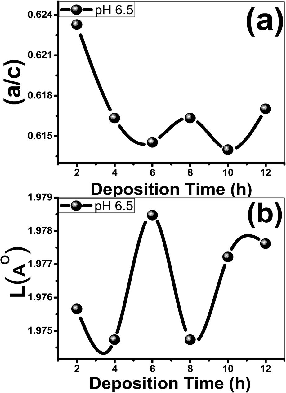 | ||
| Fig. 2 (a) The (a/c) ratio and (b) the bond length, L (Å) of the films as a function of the deposition time. | ||
Fig. 3(a) shows the XRD patterns of ZnO nanostructured films deposited at varies pH values. It is noted that all the films exhibit polycrystalline structures with similar features as XRD patterns of Fig. 1(a).57,58
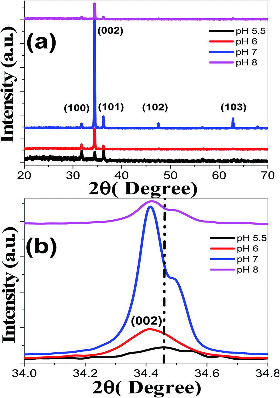 | ||
| Fig. 3 (a) XRD spectra of nanostructured ZnO films deposited at different pH values and (b) the (002) peak shift. | ||
No phases related to metallic Zn or Zn compounds are observed at 5.5 ≤ pH ≤ 8. This means that the change of pH values did not change the hexagonal structure of the ZnO films and the precursors were completely transformed into ZnO phase. At pH 5.5, the pattern shows sharper (100), (002), and (101) peaks with TC values of 1.004, 0.910, and 1.084, respectively. The lower values of texture coefficient reveal that the films have reasonable crystallinity, almost, without preferential orientations. With the increase of pH to 7, the (0 0 2) peaks became stronger and sharper that demonstrated the better growth and crystallization of ZnO thin films. For pH > 7, it was observed that there is a decrease in intensity along (0 0 2) direction. Fig. 3(b) reveals that the (002) peak position of ZnO has been slightly shifted to lower 2θ values by increasing pH value. Consequently, the increase of pH value leads to a shift of the characteristic peaks to lower angles and increase of the interplanar distance according to Bragg's law. Anandan and Muthukumaran67 reported (002) peak shift to lower 2θ values for the sol–gel prepared Y-doped ZnO nanopowder. Our results, therefore, indicate that our fabrication approach is an efficient method to get ZnO films free from impurity phases.
TCs values at different pH values were calculated using eqn (5) for the first three main peaks ((100), (002) and (101)) and presented in Table 1. The entire ZnO films exhibit enhanced intensities corresponding to (002) peak when compared to (100) and (101) peaks, which indicates a preferential orientation along the c-axis for TC (002) > 1 at 5.5 < pH ≤ 8. This is associated with the minimum value of the (002) surface free energy, which leads to increased number of grains along this plane.68 Then, increasing pH to 7 always encourage the growth of ZnO crystallites in the (002) direction, and the highest TC (002) value of 3.84 is achieved at pH 7. Similar results have been reported for Er, La and Yb-doped ZnO nanocrystals.69 This (002) preferred orientation, highly c-axis, is critical for ultrasonic oscillators and transducer devices.64
From Scherer's formula, the crystallite size (D) is increased from 41.41 to 68.43 nm by increasing pH from 5.5 to 7, then it decreases to 58.87 at pH 8, as shown in Table 1. Also, the values of a, c, V, u and are calculated and listed in Table 1. In addition, the influence of pH on the a/c ratio and Zn–O bond length (L) are depicted in Fig. 4.
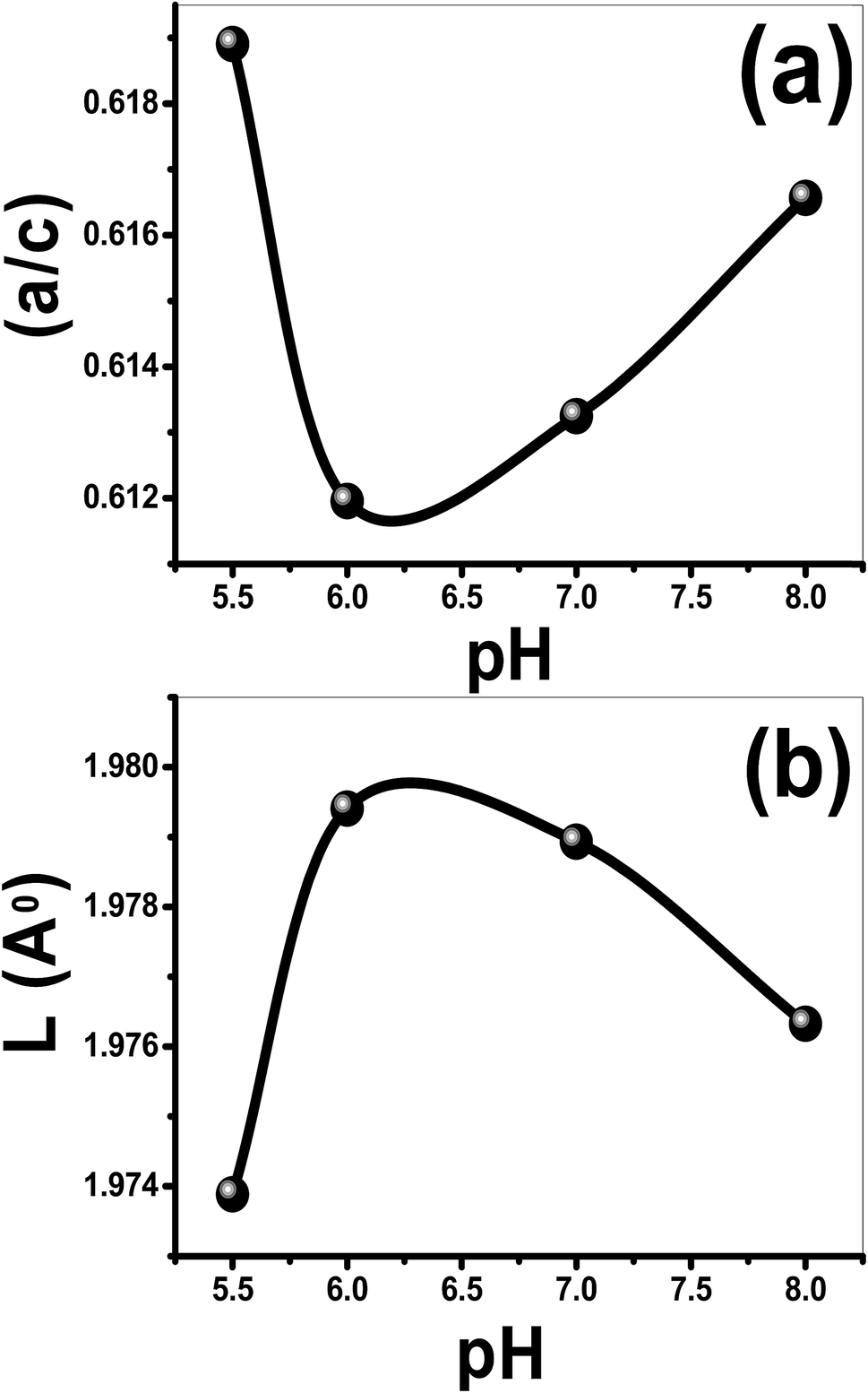 | ||
| Fig. 4 (a) The a/c ratio and (b) the bond length, L (Å), of the films as a function of the pH value. | ||
As seen from Table 1, both u parameter and the ratio a/c of the lattice parameters are affected by pH and exhibit a similar behavior. The V value of the nanostructured ZnO film is 47.4020 Å3@pH 5.5 and increased to 47.8073 Å3 with increasing pH to 6, and then decreased to 47.582 Å3 with the further increase of pH to 8. At pH 6, L increases to 1.9794 Å compared to 1.9739 Å@pH 5.5 and then decreases to 1.9763 Å@pH 8, Fig. 4(b). Also, the value of the stress is increased from 1.9606 × 10⁹@pH 5.5 to 6.6713 × 10⁹ N m−2@pH 6 and then decreased to 3.67693 × 10⁹ N m−2@pH 8. Additionally, the negative sign of the estimated stress values, Table 1, for the films indicates that the crystallites of all films are under a state of compressive stress.
From the previous results, it can be concluded that a proper deposition time and pH can significantly improve the crystalline quality of nanostructured ZnO thin films. This may be interpreted in terms of the decrease in surface energy as the ZnO atoms are trapped at or migrate down the grain boundaries.70
3.2. Chemical composition
SEM/EDX spectroscopy is the best widely-used of the surface analytical techniques since it is inexpensive, relatively rapid, and basically a non-destructive approach to surface analysis. The analysis of the emitted EDX signals from the samples gives the quantitative elemental information. Fig. 5 shows the energy dispersive X-ray (EDX) spectra of ZnO nanostructures deposited at 8 h and (a) pH 6.5 and (b) pH 7. The quantitative analyses of the chemical composition of the fabricated ZnO thin films are shown in the inset tables. The EDX spectra clearly confirm the presence of Zn and O peaks. There are three peaks relevant to Zn at around 1, 8.6, and 9.6 keV. In addition, Si, Ca, and Al signals are detected from the glass substrate in the EDX pattern. This is because EDX has a larger interaction volume than the thickness of the ZnO film. As the pH value is increased from 6.5 to 7, almost all the traces signal from the substrate disappeared. The quantitative analysis of the ZnO at pH 6.5 is 84.7% Zn and 15.3% O, which indicates the high purity of the fabricated ZnO thin film. Also, these ratios are very close to the ideal stoichiometric ratio between Zn and O atoms. By increasing pH to 7, the Zn/O ratio is increased as the pH value increased to 7. Therefore; the chart in Fig. 5(a) shows that the O signal not only comes from the ZnO thin film but also from the glass substrate.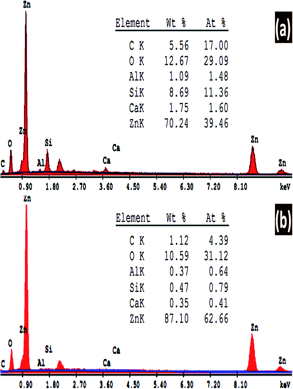 | ||
| Fig. 5 EDX spectra of ZnO nanostructured films deposited at 8 h and pH (a) 6.5 and (b) pH 7. | ||
3.3. Surface morphological analysis
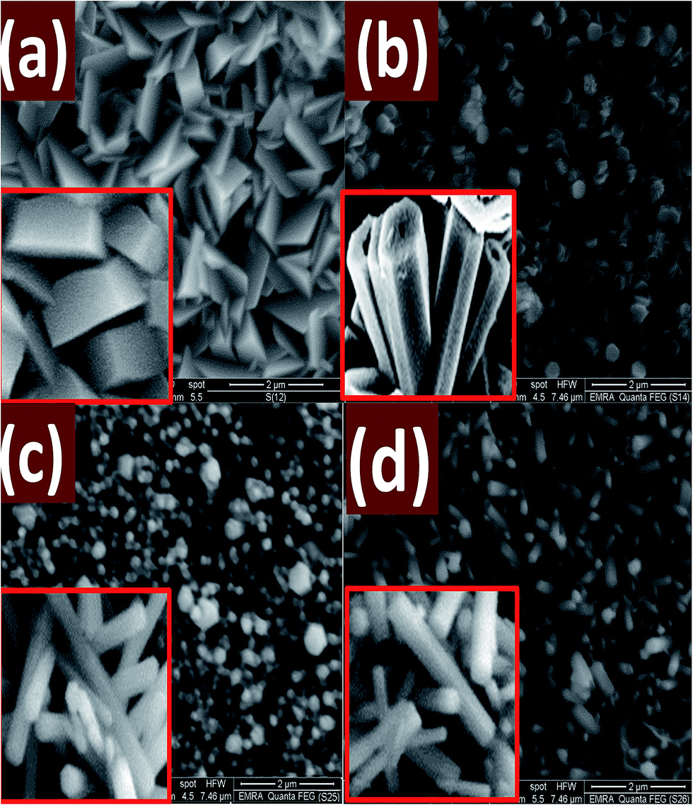
Fig. 6 shows SEM images of ZnO thin films grown on ZnO seed layer by chemical bath deposition technique with different reaction time: (a) 2, (b) 4, (c) 6, (d) 8, (e) 10, and (f) 12 h. As shown, ZnO nanostructures undergo a gradual morphological evolution with reaction time.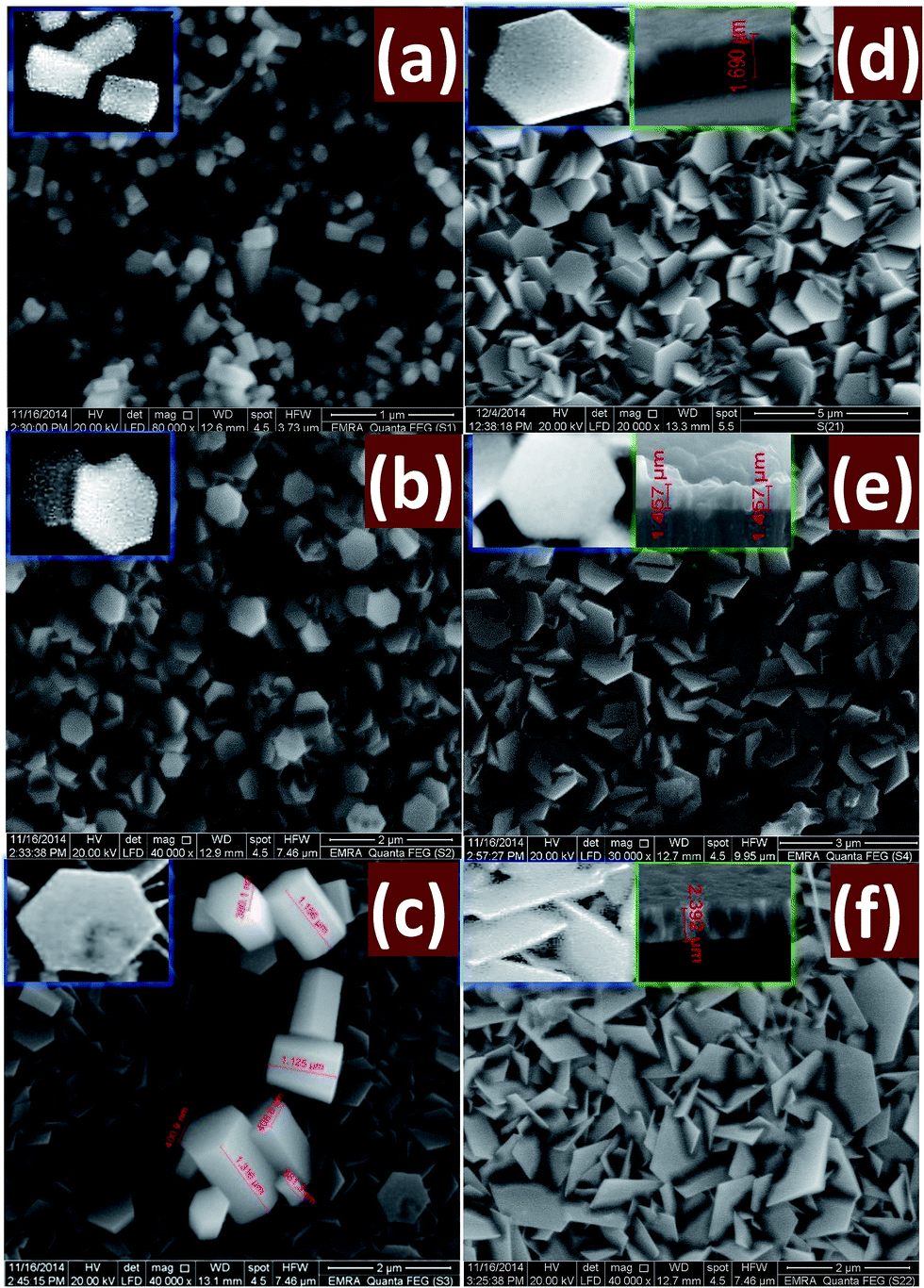 | ||
| Fig. 6 SEM images of nanostructured ZnO thin films deposited at different times (a) 2, (b) 4, (c) 6, (d) 8, (e) 10 and (f) 12 h. The insets showed magnified and cross-sectional SEM images. | ||
When the deposition has been performed for 2 h, Fig. 6(a), nanorods of random distribution was formed. The disordered growth of ZnO nanorods is due to the nature of the polycrystalline glass substrate. All of the ZnO nanorods display a perfect hexagonal shape throughout their lengths as shown in the SEM image and grow preferentially along the c-axis direction. These nanorods displayed average diameter and length of ∼200 and 600 nm, respectively.
Fig. 6(b) displays SEM image of ZnO nanostructured film grown-up for 4 h. A random distribution of hexagonal nanodiscs was formed and accompanied with a few numbers of ZnO nanorods distributed in the ZnO film. The nanorods have average diameter 400 nm and average length 480 nm. The morphology study of the grown ZnO film for 6 h, Fig. 1(c), shows a high density of hexagonal nanodisc formed with a very small number ZnO nanorods spread on the film surface. The ZnO nanodisc takes different and random directions. As the deposition time is prolonged to 8 h, some cracks appear and the number of nanodiscs increase. Then, the simultaneous growth of an enormous number of nanodiscs limits their sizes and leads to strong interfere between these nanodiscs. Also, the nanorods are disappeared at the longer deposition time, Fig. 1(d). The SEM images 1(a–c) clearly refer to the decrease of the ZnO nanorods density and the complete conversion from hexagonal nanorods into hexagonal nanodisc as the growth time increases. I. e., nanorods numbers decrease and numbers of nanodiscs increase as the time of deposition increased. For tD > 8 h, Fig. 1(e and f), the density and surface area of the hexagonal nanodiscs is increased as the deposition time increased. As the deposition time increased, the discs become thin and interfere with each other. Also, the homogeneity of the film is improved due to the uniform agglomeration of the discs which agrees well with the decrease of the stress values as depicts from XRD calculations Table 1. In addition, the increase of surface area of the hexagonal discs as the deposition time increased is consistent with XRD results that revealed the growth of the crystallite size from 63.4 to 65.6 nm with increasing deposition time from 10 to 12 h. One of the important notes is that the measured sizes by FE-SEM appear to be greater than that calculated by XRD. This suggests that FE-SEM gives the rod or disc size that may be consisted of more than one crystallite, while the XRD gives the crystallite size.
Fig. 7 shows the variation of the film thickness in μm with the deposition time. As shown there are three regimes for the increase of the film thickness. The thickness of the samples was increased from 582.8 nm at 2 h to 1.4 μm at 8 h and 2.392 μm at 12 h. Then, the vertical growth rate is decreased from 4.86 nm min−1 at 2 h to ∼3.04 nm min−1 at 8 h, and then increased again to 5.85 nm min−1 as the growth time increased from 8 to 12 h.
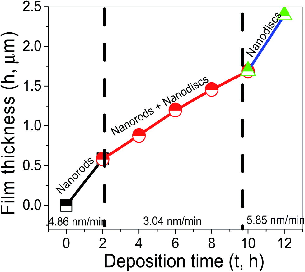 | ||
| Fig. 7 Variation of film thickness with deposition time. | ||
The same result was obtained in a previous study by growing the concentration of OH− in the precursor.65 When the OH− concentration is low, the crystal growth rate along the c axis is faster than the growth rate alongside any other direction. Therefore, the ZnO sample shows the morphology of one-dimensional nanorods. At high OH− concentrations in the precursor, the (001) surfaces of ZnO with tetrahedral zincs, usually, have terminal OH− ligands in solution.71,72 These ligands will prevent the newly produced ZnO clusters from the effective progression on the ZnO crystallites. Therefore, the crystal growth of the ZnO crystallites along the c axis is partially suppressed under this condition. However, they can still grow sideways and finally two-dimensional ZnO nanoplates are formed. In our experiment, ammonia reacts with water to produce ammonium hydroxide, which provides a continuous source of OH− for hydrolysis. Then, the concentration of OH− in the solution is increased as the growth time increased. Hence, the hexagonal nanorods (Fig. 1(a)) are converted into hexagonal nanodisc (Fig. 1(c)). These results revealed that the growth duration plays an important role in the morphology of the ZnO nanostructures. The ZnO nanorod size increases and the nanorods densities decrease when increasing the deposition time due to the Ostwald ripening.73
Fig. 8 shows FE-SEM images of ZnO nanostructured films deposited at pH 5.5, 6, 7, and 8 for 8 h. As it can be seen, the film deposited at pH 5.5 revealed well-defined morphology with stacked hexagonal slices or plate-like structures. Fig. 8(b) shows hexagonal plates with a random distribution of flower-like structure made up of the submicron rod-like structure. At pH 7, the morphology of the deposited ZnO film, Fig. 8(c), is almost hexagonal nanorods of average diameter 170 nm with a few number of nanodiscs. At pH 8, Fig. 8(d), random distribution of hexagonal nanowires of different diameters is observed and vertically grown from the seeds on the glass substrate. Note that; the nanodiscs are completely disappeared. The length of the nanowires at pH 8 is higher than the length of the nanorods that grown at pH 7. For 9 ≤ pH ≤ 5, the seed layer is etched, and no ZnO nanostructures are grown by this technique.
 | ||
| Fig. 8 FE-SEM micrographs for nanostructured ZnO films deposited at different pH values; (a) 5.5, (b) 6, (c) 7, and (d) 8 for 8 h. The insets show corresponding cross-sectional FE-SEM images. | ||
3.4. Optical properties
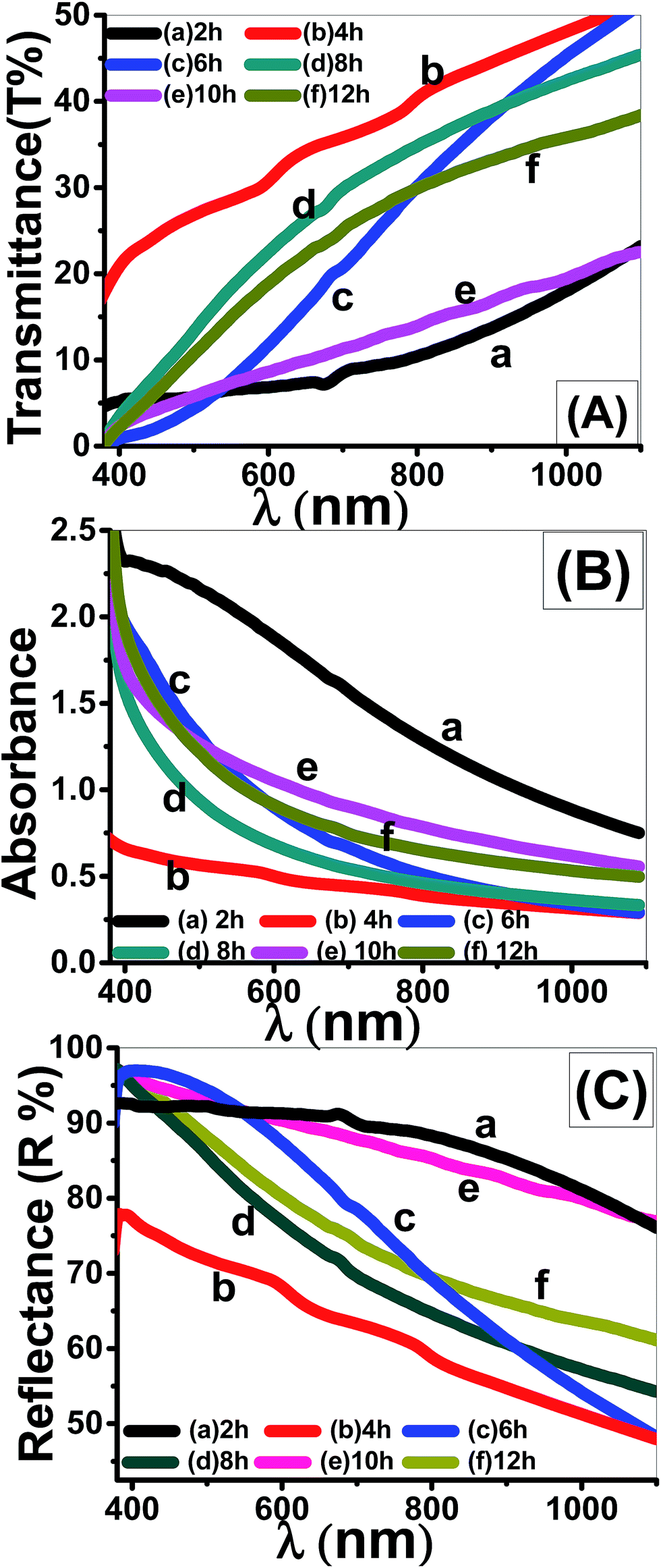 | ||
| Fig. 9 Optical spectra of nanostructured ZnO thin films deposited at different times; (A) transmittance, (B) absorbance, and (C) reflectance spectra. | ||
In most of the visible region of the spectra, T% is increased from 18% to 40% for the four-layered film. However, T% values of 2 layers' film increased from 5% to 10% by increasing the incident wavelength. For wavelength λ > 800 nm, the A% values of all films that deposited at a time greater than 2 h are smaller and close to zero.42 Also, it is observed that the absorption edge shifts to longer wavelengths with increasing the deposition time. This observation represents the first indication of the tuning the optical band gap (Eg) of ZnO films after particular deposition time.
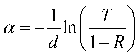
Using the recorded transmission (T) and reflection (R) spectra, the absorption coefficient (α) was calculated using the general expression:74
 | (11) |
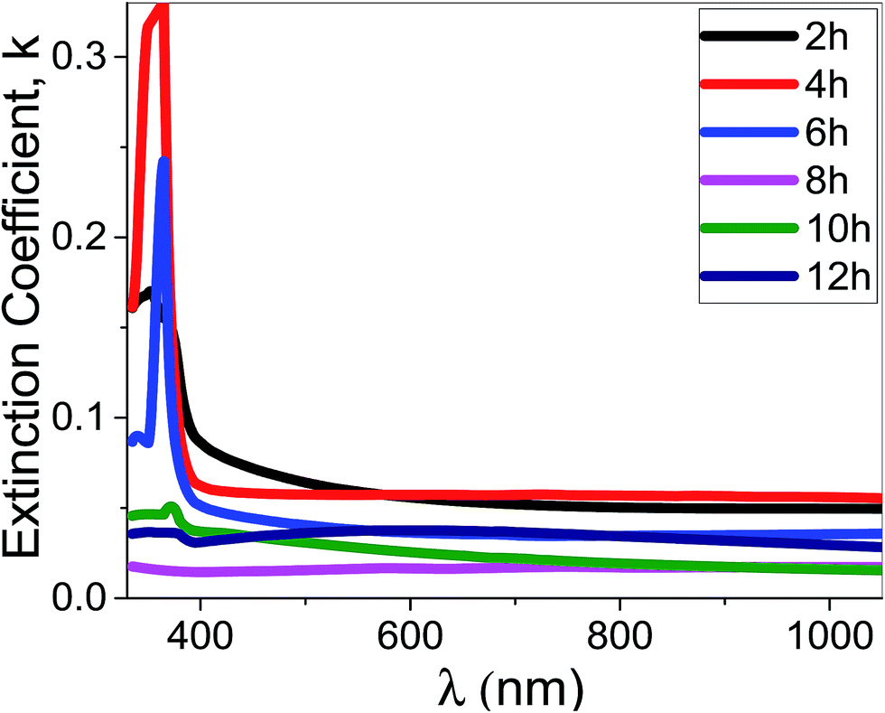 | ||
| Fig. 10 The extinction coefficient for the synthesized films at different deposition time as a function of the wavelength. | ||
The optical band gap energies can be estimated on according to the following equation, assuming direct transitions between the valence and the conduction bands.20,76
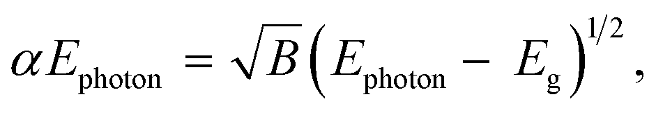 | (12) |
 | (13) |
 | ||
| Fig. 11 The plots of (a) (αhν)2 & hν to determine Eg values and (b) ln(α) & hν to determine to determine the Urbach energy of ZnO films of different morphologies. | ||
| Deposition time/pH | Eg (eV) | EU (meV) | k@λ = 500 nm | WCA(Θ) | |
|---|---|---|---|---|---|
| Deposition time effect@pH 6.5 | 2 h | 2.45 | 797 | 0.06405 | 35 |
| 4 h | 2.71 | 430 | 0.05734 | 40 | |
| 6 h | 2.88 | 728 | 0.04047 | 85 | |
| 8 h | 3.62 | 836 | 0.01543 | 135 | |
| 10 h | 3.09 | 587 | 0.03085 | 68 | |
| 12 h | 2.78 | 108 | 0.03596 | 50 | |
| pH effect@8 h | 5.5 | 2.72 | 258 | 0.04902 | 30 |
| 6 | 2.88 | 828 | 0.02563 | 86 | |
| 7 | 3.02 | 65 | 0.06243 | 45 | |
| 8 | 2.78 | 510 | 0.03484 | 23 | |
Urbach energy (EU) refers to the width of the exponential absorption edge (the tail) and can be calculated by the following relations:19,79
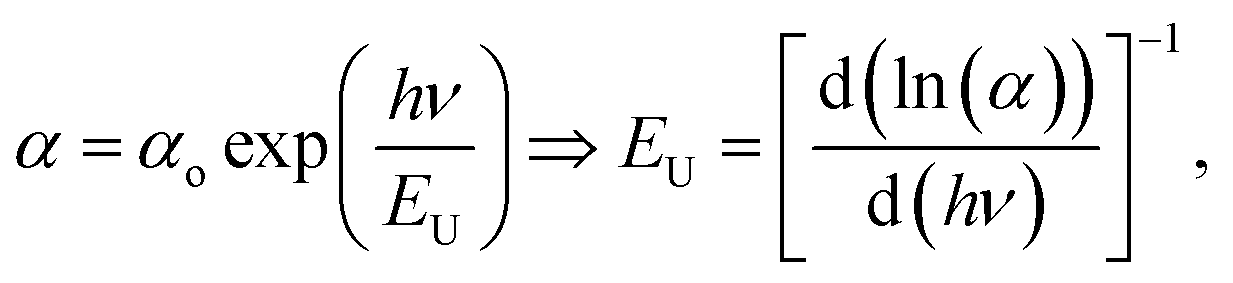 | (14) |
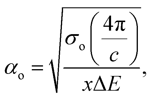 | (15) |
 | ||
| Fig. 12 Optical (A) transmittance, (B) absorbance, and (C) reflectance spectra of nanostructured ZnO thin films fabricated at different pH values. | ||
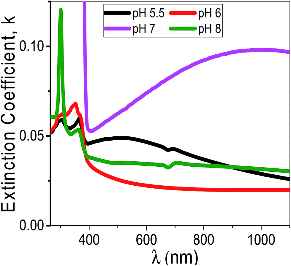
Using eqn (11), the α values were calculated and used to determine the extinction coefficient (k = αλ/4π) of the films at different pH values. Fig. 13 shows the dependence of k values of the films that fabricated at different pH values on the wavelength. At pH 7, a clear absorption edge is observed at 385 nm, whereas the other films are showed two bands centered at 305 and 360 nm. The band at 305 nm is significantly enhanced as the pH value increased. The k values sharply decrease with increasing λ in the UV region. In the visible region, k values are altered between 0.02 and 0.05 except at pH 7 the k values increased exponentially to 0.1.
 | ||
| Fig. 13 The extinction coefficient for the synthesized films at different pH values as a function of the wavelength. | ||
Using eqn (12), the energy intercept of the plots of (αhν)2 vs. hν yields Eg for a direct transition, as shown in Fig. 14(a). The corresponding Eg values at different pH values are listed in Table 2 and plotted in Fig. 14(b) as a function of the pH value. As seen from Fig. 14(b) and Table 2, the Eg of nanostructured ZnO films is blue shifted from 2.72 to 3.62 eV as the pH value increased from 5.5 to 6.5, and then red-shifted to 2.78 eV as the pH value increased to 8. Tuning the Eg values of ZnO films by controlling the pH value and hence the film morphology may, therefore, be used for broadening the optoelectronic and photovoltaic applications of these films.
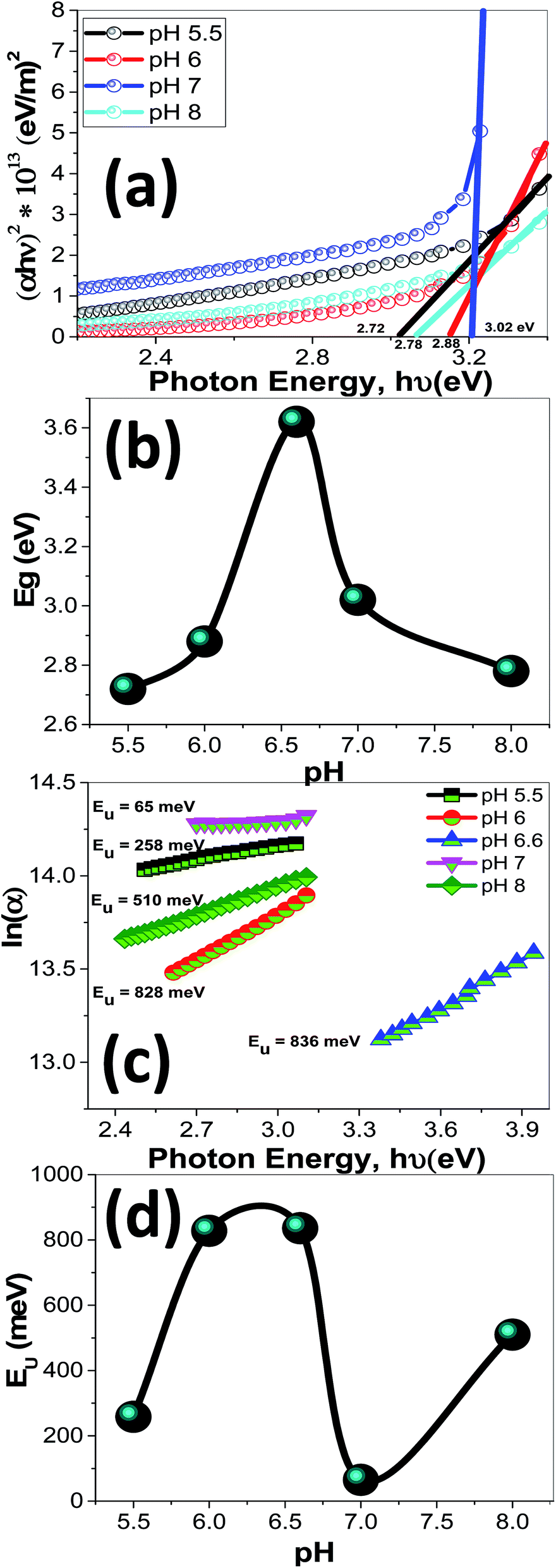 | ||
| Fig. 14 The plots of (a) (αhν)2 & hν to determine Eg values, (b) Eg as a function of pH, (c) ln(α) & hν to determine Urbach energy (EU), and (d) EU as a function of pH for nanostructured ZnO films. | ||
Fig. 14(c) shows the plots of ln(α) vs. hν. The values of the EU were obtained from the slopes of the linear fitting of this figure. The obtained EU values are listed in Table 2 and plotted in Fig. 14(d). The minimum EU, 65 meV is obtained at pH 7 and the maximum value, 836 meV, is obtained at pH 6.5. The EU is attributed to the disorder in the material that leads to the tail in the valence and conduction bands.81 Therefore, this is consistent with the XRD results, where the crystallinity enhancement is related to the decrease in the defects and charge carriers and vice versa.72 Also, this is consistent with the highly ordered nanorods morphology that obtained at pH 7.
3.5. Contact angle measurements
Wettability is a very important property governed by the geometrical structure and chemical composition of solid surfaces.82,83 However, to fully utilize the hydrophobic properties of nanostructured surfaces, it is necessary to study the fundamental relationship between the different nanostructure and the hydrophobic behavior.Two theoretical models (Wenzel model and Cassie–Baxter model) form the basic guidelines for the study of the hydrophobic surface.84,85 For a liquid drop on a solid surface, the contact angle, Θ, is determined by the surface free energies involved:20
|
cosΘ = (γsv − γsl)/γlv
| (16) |
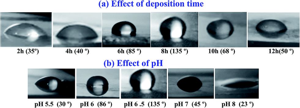 | ||
| Fig. 15 Contact angles photographs for ZnO nanostructured films fabricated at different (a) deposition time and (b) pH value. | ||
These results could be ascribed to the crystallinity and microstructural changes that occur by tuning the deposition time and pH value. A high surface energy material directly formed a hydrophilic surface.82 The three lowest density of the surface free energy is 9.9, 12.3 and 20.9 eV nm−2 for (002), (110) and (100) plans, respectively.87 The preferred orientation along (002) direction seen in ZnO films significantly decreased after 8 h deposition time and pH value 6.5. This means that the crystallinity deterioration leads to increase of the surface free energy of the films at higher pH value and hence reducing Θ values. Moreover, it was reported that the wettability of a surface can be enhanced by increasing the surface roughness within a special size range because the air trapped between the water droplet and the solid surfaces can minimize the contact angle.88 This support our data as there are changes in the surface morphology (as seen in Fig. 6 and 8) due to the change of the deposition time and the pH value. Similar results were reported for ZnO nanorods89 and thin films prepared by radio-frequency (RF) magnetron sputtering.31
4 Conclusion
ZnO nanostructured thin films of different morphologies were successfully grown on glass substrates at different conditions by a simple two-step wet chemical method. A low-cost successive ionic layer adsorption and reaction (SILAR) method was used to grow ZnO seed layers at 80 °C. Then, different hierarchical based ZnO nanostructured thin films were deposited onto the ZnO seed layers by chemical bath deposition (CBD). The influence of deposition time (tD) and pH on the surface morphology, wettability behavior, structural and optical properties of the ZnO nanostructured films were systematically investigated. The structural and morphological properties were studied by X-ray diffraction (XRD) and field emission scanning microscopy (FE-SEM). The optical and wetting properties were investigated by UV-Vis spectrophotometer and water contact angle measurement, respectively. The study of the surface morphology revealed a complex and orientated hierarchical based ZnO nanostructured films with diverse shapes from hexagonal nanorods to hexagonal nanoplates or nanodiscs and even much more complex discs/rods and flower-like shapes by changing deposition time and pH of the precursor. XRD results confirm the synthesis of nanostructured ZnO of the hexagonal structure with a preferential orientation along (002) lattice plane. The average crystallite size, D, is increased from 47.7 to 68.43 nm for tD ≤ 8 h and decreased to ∼63.4 nm at 10 h. Also, D value is increased from 41.41 to 68.43 nm by increasing pH from 5.5 to 7; then it decreases to 58.87 at pH 8. At pH 6.5, the films are hydrophilic for 10 h ≤ tD ≤ 6 h and hydrophobic for 6 h < tD < 10 h. The wetting properties of the films were enhanced by increasing or decreasing pH around 6.5. Morphology and thickness of ZnO nanostructure could efficiently control transmittance, absorbance, optical band gap, and the extinction coefficients of the films. The optical band gap is blue shifted from 2.45 to 3.62 eV, and the contact angle is increased from 35° to 135° ± 2 as the deposition time increased from 2 to 8 h. Also, the Optical band gap is blue shifted from 2.72 to 3.62 eV and contact angle is increased from 30° to 135° ± 2 as the pH value increased from 5.5 to 6.5. The existence of stable hydrophobic zinc oxide nanostructured films at room temperature with large-scale and band gaps around 3.62 eV supports their use in self-cleaning and gas sensing applications.Acknowledgements
This work is partially supported by the Egyptian Academy for Scientific Research & Technology (Grant No. ASRT/2013) through a project under the title “Fabrication of ZnO nanoparticles for self-cleaning applications”.Notes and references
- G. Kenanakis, E. Stratakis, K. Vlachou, D. Vernardou, E. Koudoumas and N. Katsarakis, Appl. Surf. Sci., 2008, 254, 5695–5699 CrossRef CAS.
- J. Lv, J. Zhu, K. Huang, F. Meng, X. Song and Z. Sun, Appl. Surf. Sci., 2011, 257, 7534–7538 CrossRef CAS.
- H. J. Butt, K. Graf and M. Kappl, Physics and chemistry of interfaces, Wiley-VCH; John Wiley, distributor, WeinheimChichester, 2nd rev. and enl. edn., 2006, vol. xii, p. 386 Search PubMed.
- M. A. Pietrzyk, E. Zielony, M. Stachowicz, A. Reszka, E. Płaczek-Popko, A. Wierzbicka, E. Przezdziecka, A. Droba and A. Kozanecki, J. Alloys Compd., 2014, 587, 724–728 CrossRef CAS.
- P. V. Korake, R. S. Dhabbe, A. N. Kadam, Y. B. Gaikwad and K. M. Garadkar, J. Photochem. Photobiol., B, 2014, 130, 11–19 CrossRef CAS PubMed.
- J. W. Lee, K. N. Hui, K. S. Hui, Y. R. Cho and H. Hwan Chun, Appl. Surf. Sci., 2014, 293, 55–61 CrossRef CAS.
- R. Vettumperumal, S. Kalyanaraman and R. Thangavel, J. Lumin., 2015, 158, 493–500 CrossRef CAS.
- M. Hjiri, R. Dhahri, K. Omri, L. El Mir, S. G. Leonardi, N. Donato and G. Neri, Mater. Sci. Semicond. Process., 2014, 27, 319–325 CrossRef CAS.
- E. Isbilir, Z. Serbetci and M. Soylu, Superlattices Microstruct., 2014, 67, 144–155 CrossRef CAS.
- D. Chu, Y. Zeng and D. Jiang, Mater. Lett., 2006, 60, 2783–2785 CrossRef CAS.
- S. Iwan, J. L. Zhao, S. T. Tan, S. Bambang, M. Hikam, H. M. Fan and X. W. Sun, Mater. Sci. Semicond. Process., 2015, 30, 263–266 CrossRef CAS.
- S. Gowrishankar, L. Balakrishnan and N. Gopalakrishnan, Ceram. Int., 2014, 40, 2135–2142 CrossRef CAS.
- Y. C. Lin, C. H. Chang, C. H. Shen, P. W. Wang and Y. C. Lee, Thin Solid Films, 2010, 518, 6055–6060 CrossRef CAS.
- M. Soylu and O. Savas, Mater. Sci. Semicond. Process., 2015, 29, 76–82 CrossRef CAS.
- N. Kiomarsipour and R. S. Razavi, Ceram. Int., 2014, 40, 11261–11268 CrossRef CAS.
- L. Y. Lin, H. J. Kim and D. E. Kim, Appl. Surf. Sci., 2008, 254, 7370–7376 CrossRef CAS.
- V. Kekkonen, A. Hakola, T. Kajava, E. Sahramo, J. Malm, M. Karppinen and R. H. A. Ras, Appl. Phys. Lett., 2010, 97, 044102 CrossRef.
- J. Tam, G. Palumbo and U. Erb, Materials, 2016, 9, 151 CrossRef.
- M. Shaban and A. M. El Sayed, Mater. Sci. Semicond. Process., 2016, 41, 323–334 CrossRef CAS.
- M. Shaban and A. M. El Sayed, Mater. Sci. Semicond. Process., 2015, 39, 136–147 CrossRef CAS.
- K. Thirumalai, E. T. D. Kumar, R. Aravindhan, J. R. Rao and M. Swaminathan, Surfaces and Interfaces, 2016, 5, 30–38 CrossRef.
- O. Akhavan, M. Mehrabian, K. Mirabbaszadeh and R. Azimirad, J. Phys. D: Appl. Phys., 2009, 42, 225305 CrossRef.
- P. S. Kumar, J. Sundaramurthy, D. Mangalaraj, D. Nataraj, D. Rajarathnam and M. P. Srinivasan, J. Colloid Interface Sci., 2011, 363, 51–58 CAS.
- X. W. Sun, J. Z. Huang, J. X. Wang and Z. Xu, Nano Lett., 2008, 8(4), 1219–1223 CrossRef CAS PubMed.
- V. P. Verma, H. Jeon, S. Hwang, M. Jeon and W. Choi, IEEE Trans. Nanotechnol., 2008, 7(6), 782–786 CrossRef.
- Z. Guo, X. Chen, J. Li, J. H. Liu and X. J. Huang, Langmuir, 2011, 27, 6193–6200 CrossRef CAS PubMed.
- J. M. Szarko, J. K. Song, C. W. Blackledge, I. Swart, S. R. Leone, S. Li and Y. Zhao, Chem. Phys. Lett., 2005, 404, 171–176 CrossRef CAS.
- J. B. Baxter, A. M. Walker, K. vam Ommering and E. S. Aydil, Nanotechnology, 2006, 17, 304–312 CrossRef.
- L. Zhang, L. Yin, C. Wang, N. Lun and Y. Qi, ACS Appl. Mater. Interfaces, 2010, 2, 1769–1773 CAS.
- P. Sangpour, M. Roozbehi, O. Akhavan and A. Z. Moshfegh, Curr. Nanosci., 2009, 5, 479–484 CrossRef CAS.
- P. W. Chi, C. W. Su, B. H. Jhuo and D. H. Wei, Int. J. Photoenergy, 2014, 1–10, 765209, DOI:10.1155/2014/765209.
- M. Reza Khanlary, V. Vahedi and A. Reyhani, Molecules, 2012, 17, 5021–5029 CrossRef PubMed.
- J. Lim and C. Lee, Thin Solid Films, 2007, 515, 3335–3338 CrossRef CAS.
- L. Armelao, M. Fabrizio, S. Gialanella and F. Zordan, Thin Solid Films, 2001, 394, 89–95 CrossRef.
- C. Hock Ong, J. Hui Wang, H. Gong and H. S. O. Chan, Int. J. Mod. Phys. B, 2002, 16, 314–321 CrossRef.
- T. Sisianu, O. Lupan, S. Sisianu, S. Railean and V. Besliu, Proceedings of the Third International Conference on Microelectronics and Computer Science, 1, ICMCS-2002, 2002, pp. 292–296 Search PubMed.
- I. Stambolova, K. Konstantinov, S. Vassilev, P. Peshev and T. Tsacheva, Mater. Chem. Phys., 2000, 63(2), 104–108 Search PubMed.
- D. J. Qiu, H. Z. Wu, A. M. Feng, Y. F. Lao, N. B. Chen and T. N. Xu, Appl. Surf. Sci., 2004, 222, 263–268 CrossRef CAS.
- M. Purica, E. Budianu, E. Rusu, M. Danila and R. Gavrila, Thin Solid Films, 2002, 403–404, 485–488 CrossRef CAS.
- T. P. Niesen and M. R. De Guire, Solid State Ionics, 2002, 151, 61–68 CrossRef CAS.
- Y. F. Nicolau, Appl. Surf. Sci., 1985, 22–23, 1061–1074 CrossRef CAS.
- K. Govender, D. S. Boyle, P. B. Kenway and P. O'Brien, J. Mater. Chem., 2004, 14, 2575–2591 RSC.
- P. K. Giri, S. Dhara and R. Chakraborty, Mater. Chem. Phys., 2010, 122, 18–22 CrossRef CAS.
- H. Zhu, H. Jia, D. Liu, Y. Feng, L. Zhang, B. Lai, T. He, Y. Ma, Y. Wang, J. Yin, Y. Huang and Y. Mai, Appl. Surf. Sci., 2012, 258, 6018–6023 CrossRef CAS.
- K. Govender, D. S. Boyle, P. B. Kenway and P. O'Brien, J. Mater. Chem., 2004, 14, 2575–2591 RSC.
- Y. Liu, X. Chen and J. H. Xin, Nanotechnology, 2006, 17, 3259–3263 CrossRef CAS.
- W. Zhang, P. Wang, X. Fei, Y. Xiu and G. Jia, Int. J. Electrochem. Sci., 2015, 10, 4688–4695 CAS.
- F. P. Albores, F. P. Delgado, W. A. Flores, P. A. Madrid, E. R. Valdovinos and M. Yoshida, J. Nanomater., 2011, 643126, 11 Search PubMed.
- E. L. Papadopouloua, V. Zorbab, A. Pagkozidisa, M. Barberogloua, E. Stratakisa and C. Fotakisa, Thin Solid Films, 2009, 518, 1267–2127 CrossRef.
- T. Wanga, L. Changa, S. Yanga, Y. Jiaa and C. Wongb, Ceram. Int., 2013, 397, 8165–8172 CrossRef.
- R. Mimounia, N. Mahdhib, K. Boubakera, A. Madouric and M. Amlouka, Superlattices Microstruct., 2016, 91, 345–357 CrossRef.
- S. Patra, S. Sarkar, S. K. Bera, R. Ghosh and G. K. Paul, J. Phys. D: Appl. Phys., 2009, 42, 075301 CrossRef.
- V. R. Shindea, C. D. Lokhandea, R. S. Maneb and S. H. Hanb, Appl. Surf. Sci., 2005, 245, 407–413 CrossRef.
- Z. Lia, K. Zhua, Q. Zhaob and A. Mengb, Appl. Surf. Sci., 2016, 377, 23–29 CrossRef.
- P. Suresh Kumara, A. Dhayal Raja, D. Mangalarajb and D. Nataraja, Thin Solid Films, 2010, 518, 183–186 CrossRef.
- Y. You Wanga, G. Qiang Zhoua, J. Guoa and T. Qing Liua, Ceram. Int., 2016, 42, 12467–12474 CrossRef.
- V. Şenaya, S. Patb, Ş. Korkmazb, T. Aydoğmuşb, S. Elmasb, S. Özenb, N. Ekemb and M. Zafer Balbağc, Appl. Surf. Sci., 2014, 318, 2–5 CrossRef.
- R. Mariappan, V. Ponnuswamy, P. Suresh, R. Suresh and M. Ragavendar, Superlattices Microstruct., 2013, 59, 47–59 CrossRef CAS.
- M. Soylu and O. Savas, Mater. Sci. Semicond. Process., 2015, 29, 76–82 CrossRef CAS.
- C. Suryanarayan and M. Grant Norton, X-Ray Diffraction: A Practical Approach, Plenum Press, New York, 1998 Search PubMed.
- M. Ashokkumar and S. Muthukumaran, JOL, 2014, 145, 167–174 CAS.
- D. Li, J. Feng Huang, L. Yun Cao, J. Yin Li, H. Boou Yang and C. Yan Yao, Ceram. Int., 2014, 40, 2647–2653 CrossRef CAS.
- L. W. Wang, F. Wu, D. X. Tian, W. J. Li, L. Fang, C. Y. Kong and M. Zhou, J. Alloys Compd., 2015, 623, 367–373 CrossRef CAS.
- A. Taabouche, A. Bouabellou, F. Kermiche, F. Hanini, Y. Bouachiba, A. Grid and T. Kerdjac, Mater. Sci. Semicond. Process., 2014, 28, 54–58 CrossRef CAS.
- M. Shaban, M. Mustafa and A. M. El Sayed, Mater. Sci. Semicond. Process., 2016, 56, 329–343 CrossRef CAS.
- J. A. Mary, J. J. Vijaya, J. H. Dai, M. Bououdina, L. J. Kennedy and Y. Song, Mater. Sci. Semicond. Process., 2015, 34, 27–38 CrossRef.
- S. Anandan and S. Muthukumaran, Opt. Mater., 2013, 35, 2241–2249 CrossRef CAS.
- L. W. Wang, F. Wu, D. X. Tian, W. J. Li, L. Fang, C. Y. Kong and M. Zhou, J. Alloys Compd., 2015, 623, 367–373 CrossRef CAS.
- R. Zamiri, A. F. Lemos, A. Reblo, H. A. Ahangar and J. M. F. Ferreira, Ceram. Int., 2014, 40, 523–529 CrossRef CAS.
- R. Mimouni, K. Boubaker and M. Amlouk, J. Alloys Compd., 2015, 624, 189–194 CrossRef CAS.
- J. Slunec ko, M. Kosec, J. Holc and G. Drazic, J. Am. Ceram. Soc., 1998, 81, 1121–1124 CrossRef CAS.
- P. K. Dutta, P. K. Gallagher and J. Twu, Chem. Mater., 1992, 4, 847–851 CrossRef CAS.
- O. Krichershy and J. Stavan, Phys. Rev. Lett., 1993, 70, 1473–1477 CrossRef PubMed.
- Y. Dongliang, G. Chuannan and D. Youwei, J. Semicond., 2009, 30, 072003 CrossRef.
- A. M. El Sayeda and M. Shaban, Spectrochim. Acta, Part A, 2015, 149, 638–646 CrossRef PubMed.
- M. Moustafaa, A. Paulheima, M. Mohameda, C. Janowitza and R. Manzkea, Appl. Surf. Sci., 2016, 366, 397–403 CrossRef.
- M. S. Jiang, Q. Mei Sui, Z. Wei Jin, F. Y. Zhang and L. Jia, Optik, 2014, 125, 3295–3298 CrossRef CAS.
- L. Aïnouchea, L. Hamadoua, A. Kadria, N. Benbrahima and D. Bradaib, Sol. Energy Mater. Sol. Cells, 2016, 151, 179–190 CrossRef.
- R. Mimouni, K. Boubaker and M. Amlouk, J. Alloys Compd., 2015, 624, 189–194 CrossRef CAS.
- S. Sharma, S. Vyas, C. Periasamy and P. Chakrabarti, Superlattices Microstruct., 2014, 75, 378–389 CrossRef CAS.
- A. M. El Sayed and A. Ibrahim, Mater. Sci. Semicond. Process., 2014, 26, 320–328 CrossRef CAS.
- J. Lv, J. Zhu, K. Huang, F. Meng, X. Song and Z. Sun, Appl. Surf. Sci., 2011, 257, 7534–7538 CrossRef CAS.
- J. Hu, Y. Sun, W. Zhang, F. Gao, P. Li, D. Jiang and Y. Chen, Appl. Surf. Sci., 2014, 317, 545–551 CrossRef CAS.
- R. N. Wenzel, Ind. Eng. Chem. Res., 1936, 28, 988 CrossRef CAS.
- A. B. D. Cassie and S. Baxter, J. Chem. Soc., Faraday Trans., 1944, 40, 546 RSC.
- P. S. Kumar, J. Sundaramurthy, X. Zhang, D. Mangalaraj, V. Thavasi and S. Ramakrishna, J. Alloys Compd., 2013, 553, 375–382 CrossRef CAS.
- L. W. Wang, F. Wu, D. X. Tian, W. J. Li, L. Fang, C. Y. Kong and M. Zhou, J. Alloys Compd., 2015, 623, 367–373 CrossRef CAS.
- H. Luo, J. Ma, P. Wang, J. Bai and G. Jing, Appl. Surf. Sci., 2015, 347, 868–874 CrossRef CAS.
- A. Yumak, G. Turgut, O. Kamoun, H. Ozisik, E. Deligoz, P. Petkova, R. Mimouni, K. Boubaker, M. Amlouk and S. G. Said, Mater. Sci. Semicond. Process., 2015, 39, 103–111 CrossRef CAS.
| This journal is © The Royal Society of Chemistry 2017 |