
Growth and humidity-dependent electrical properties of bulk-like MoS2 thin films on Si
Y. J. Liua,
L. Z. Hao*a,
W. Gaoa,
Y. M. Liua,
G. X. Lia,
Q. Z. Xue*a,
W. Y. Guoa,
L. Q. Yua,
Z. P. Wub,
X. H. Liub,
H. Z. Zengb and
J. Zhub
aCollege of Science, China University of Petroleum, Qingdao, Shandong 266580, People's Republic of China. E-mail: haolanzhong@upc.edu.cn; xueqz@upc.edu.cn
bState Key Laboratory of Electronic Thin Films and Integrated Devices, University of Electronic Science and Technology of China, Chengdu 610054, People's Republic of China
First published on 26th August 2015
Abstract
Bulk-like molybdenum disulfide (MoS2) thin films were deposited on Si substrates using a dc magnetron sputtering technique and n-MoS2/p-Si junctions were fabricated at room temperature (RT) and 400 °C, respectively. The typical oscillating modes of E12g and A1g were shown in the Raman spectra of the as-grown MoS2 films. Atomic force microscopy illustrated that the surfaces of the films were composed of dense nanoscale grains and scanning electron microscopy revealed the existence of large quantities of pores in the surface. The current–voltage curves of the junctions showed obvious rectifying characteristics due to the energy-band bending near the interface of MoS2/Si. The fabricated junctions exhibited humidity-dependent electrical properties. Compared with the one with the MoS2 film deposited at RT, the junction fabricated at 400 °C showed much more obvious sensing properties to humid gas. In particular, the sensitivity of the device could be tuned by external electrical fields. In the forward voltage range, the currents increased significantly after the junction was exposed to humid conditions. The response increased with increasing voltage and reached a saturated value after V = 1.9 V. The sensing performance featured high sensitivity, fast response and recovery. The junction current in the reverse voltage range decreased under the humid condition. This was contrary to that in the forward voltage range. We also studied the dependence of the sensing response on humidity levels. An almost linear correlation was obtained in the measured range of humidity levels. The sensing mechanisms of the MoS2/Si heterojunction were proposed.
I Introduction
Due to its good electrical, mechanical and optical properties, molybdenum disulfide (MoS2) has been studied widely in recent years.1 MoS2 has become an excellent candidate to develop high-performance and multifunctional electronic devices, such as transistors, sensors, and solar cells.2–4 As one kind of focused electronic material, the dependence of its electrical properties on the surrounding conditions has drawn considerable attention. Recently, many researchers have focused on the effect of atmospheric humidity on the electrical characteristics of nano materials such as MoS2 nanoflakes, graphene, carbon films, and polymers.5–8 The studied results show that humidity gas can increase or decrease the electrical resistance of nanoscale materials monotonically. MoS2-based nanoscale materials are a kind of versatile materials applied in various fields. Thus, it is important to understand the humidity dependence of their electrical properties, not only due to its potential applications in developing new-type humidity sensors, but also due to the fact that large parts of the applications of the electronic device have to face the atmosphere circumstance where humidity influence has to be taken into account. The previous studies about MoS2-based systems are mostly focused on top- or bottom-gated field-effect transistor devices.9 In this kind of MoS2-based sensor device, the electrical properties are dominated by the in-plane conduction mechanisms and the sensing characteristics originate mainly from the single MoS2 materials. However, few p–n junction devices composed of MoS2 and conventional semiconductors (such as Si) have been reported.10 As a basic element in various kinds of electronic devices semiconductor p–n junctions have been widely used. Compared with single MoS2 material, MoS2/Si p–n junctions have two advantages. Firstly, the excellent properties of MoS2, such as gas sensing and photoelectrical properties, could be integrated onto Si semiconductors and the fabrication of multifunctional devices would be realized.11 Secondly, novel electrical characteristics can be caused by the incorporation of the junction area near the interface.12Based on the above analysis, MoS2 thin films were grown on p-type Si substrates using magnetron sputtering technique and the n-MoS2/p-Si heterojunctions were fabricated in this study. The electrical characteristics of the fabricated junctions were investigated. We found that the currents changed largely when the MoS2/Si junctions were exposed to humidity gas at room temperature (RT) and obvious sensing properties to humidity gas were observed. Especially, the sensing behaviours could be tuned by external electrical fields.
II Experimental section
MoS2 thin films were deposited on (100)-oriented Si substrates using dc magnetron sputtering technique. The MoS2 powder (purity, 99.9%) were cold-pressed into the sputtered target. The substrates used in this work were p-type Si (1.2–1.8 Ω cm). Before the deposition, the substrates were ultrasonically cleaned in sequence by using alcohol, acetone, and de-ionized water. Then, the substrates were dipped into HF solution (∼4.0%) for 3 min to remove the amorphous SiO2 layer from the silicon surface. Subsequently, the Si substrates were immediately moved into the vacuum chamber. Then, the MoS2 thin films were deposited at RT and 400.0 °C, respectively. During the deposition, the working pressure of argon gas was kept at 1.0 Pa and the sputtering power was about 120.0 W. The film thickness of the as-prepared MoS2 thin film was about 88.1 nm. After the deposition, indium (In) ohmic electrodes were pressed on MoS2 thin films and Si, respectively. The schematic illustration of the heterojunction is shown in Fig. 1(a). The MoS2 films were also grown on insulating Si substrates and the in-plane I–V curves were measured to show the humidity sensing properties of single MoS2 films, the schematic illustration of the device based on a single MoS2 film is shown in Fig. 1(b). | ||
| Fig. 1 Schematic illustration of the electrical measurement of (a) MoS2/Si heterojunction and (b) the device based on a single MoS2 film. | ||
Samples were characterized using Raman spectroscopy (Renishaw, 514 nm laser). The surface was characterized by atomic forced microscope (AFM, SPM-300HV, SEIKO) and scanning electron microscope (SEM, JSM-7001F, JEOL). The capacitance–voltage (C–V) curves were measured using HP4284 source meter. The current–voltage (I–V) curves were measured using Keithley2400 source meter at RT. Sensing properties were measured in a chamber by exposing the MoS2/Si heterojunction to different humidity levels at RT (∼300 K).
III Results and discussion
Fig. 2(a) shows the Raman spectra of the MoS2 films on Si substrates deposited at RT and 400 °C, respectively. From the figure, we can see that both the films exhibit two characteristic MoS2 Raman peaks, the E12g mode at ∼377 cm−1 and the A1g mode at ∼403 cm−1. The separation between Raman peaks of the film, Δλ = 26 cm−1, is much larger than those for the reported monolayer and several-layer MoS2.13 Compared to the film deposited at RT, the MoS2 film deposited 400 °C shows stronger intensity of the Raman peak. This can be attributed to the improved crystallization quality of the film deposited at a higher temperature. The position of Raman peaks of the films is accord with that of the MoS2 target used in this work, as shown in Fig. 2(b). This means that the as-deposited films is bulk-like. The E12g mode corresponds to the S and Mo atoms oscillating in antiphase parallel to the crystal plane and the A1g mode corresponds to the S atoms oscillating in antiphase out-of-plane, as shown in the insets. These results are consistent with other reported results.14 | ||
| Fig. 2 (a) Raman spectra of the MoS2 films deposited on Si substrates at RT and 400 °C, respectively. (b) Raman spectrum of the MoS2 target used in this work. The insets shows the schematic illustration the oscillating mode of E12g and A1g. | ||
Fig. 3(a) shows AFM topographic image of the MoS2 thin film on Si deposited at RT. From the figure, we can see that the surface of the film is composed of some cone-like grains. The root-mean-square roughness (RMS) of the film is about 1.2 nm, and the average size of grains is about 67.9 nm in diameter. When the deposition temperature increases to 400 °C, the size of the surface grains increases obviously, as shown in Fig. 3(b). According to the measurements, the average size of grains increases 95.9 nm in diameter and the covering ratio of the grains reaches about 89.7%. The dense nano-level grains could increase the surface-to-volume ratio of the MoS2 films and this could cause the adsorption of ambient gas molecules on the surface.
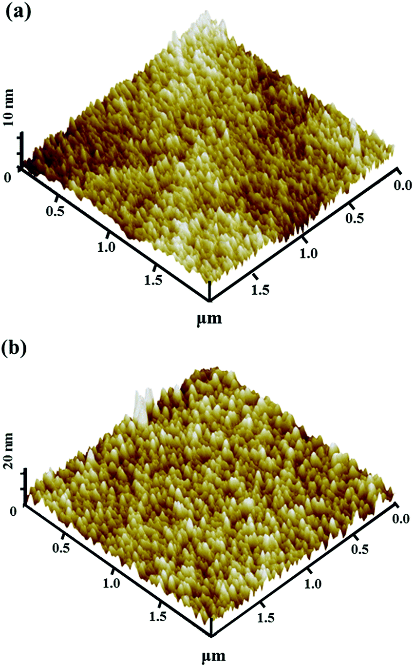 | ||
| Fig. 3 AFM surface morphology of the MoS2 thin film deposited on Si at (a) RT and (b) 400 °C, respectively. | ||
Fig. 4(a) shows the SEM micrographs of the surface of the as-grown MoS2 film deposited at RT. From the figure, large quantities of grain boundaries can be seen obviously and a porous surface is formed. Fig. 4(b) shows the SEM micrographs of the surface of the MoS2 film deposited at 400 °C. From the figures, we can see that the pore size increase largely when the deposition temperature increases from RT to 400 °C. These grain boundaries could supply effective routes for the absorbed gas molecules to diffuse into the film and even reach the interface area of MoS2/Si.
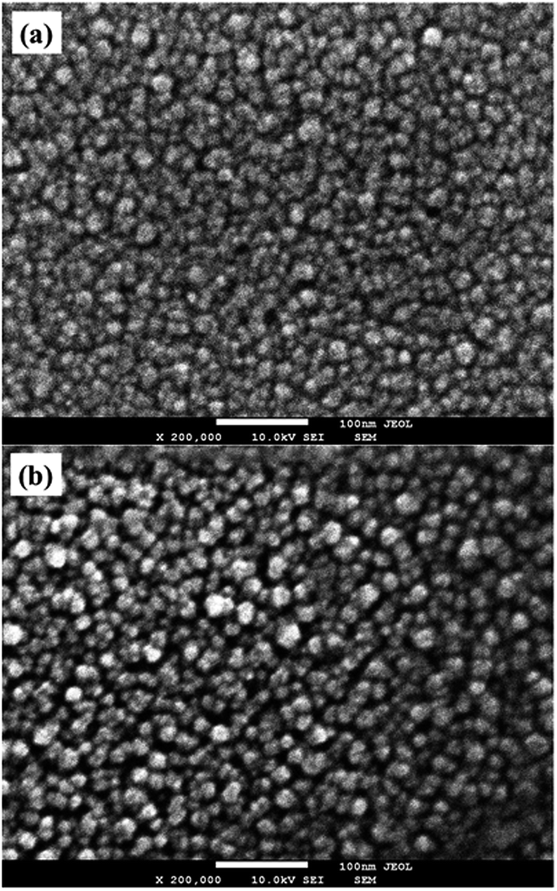 | ||
| Fig. 4 SEM micrographs of the surface morphology of the MoS2 films deposited on Si substrates at (a) RT and (b) 400 °C. | ||
Fig. 5(a) shows the I–V curve of the In/MoS2/Si/In junction at RT. The MoS2 film was deposited at 400 °C. From the figure, obvious rectifying behaviour can be seen. The rectifying ratio (I+/I−) measured at ±5.0 V is about 3.2. The inset shows the I–V curves of the In/Si and In/MoS2 contacts, respectively. From the figure, almost linear characteristics can be seen. This demonstrates that both the In/MoS2 and In/Si interfaces belong ohmic contacts. Therefore, the rectifying I–V characteristic in the device structure is mainly attributed to the MoS2/Si junction. The curve of C−3 versus reverse voltages obtained from C–V curve of the junction is shown in Fig. 5(b). The linear relationship implies that the fabricated heterojunction is graded.15 According to the intercept on voltage axis, the built-in electrical field (Vbi) can be obtained, about 0.42 V.
 | ||
| Fig. 5 (a) I–V curves of the MoS2/Si heterojunction fabricated at 400 °C. The inset shows the I–V curves of In/MoS2 and In/Si. (b) Characteristics of C−3 vs. reverse voltages obtained from C–V curve of the fabricated junction. | ||
Fig. 6(a) shows the energy band diagram of isolated MoS2 and p-Si. According to our previous studies, the MoS2 thin films deposited at 400 °C are n-type semiconductors and the energy-band gap (Eg1) is about 1.4 eV.16 For the p-Si used in our experiments, the Fermi energy level [EF2 = 5.0 eV] and energy band gap [Eg2 = 1.12 eV] are taken to construct the band structure and the difference (EF2 − EV2) between the Fermi energy level and the top of the valence band is about 0.2 eV.17 According to eVbi = EF2 − EF1,18 the Fermi energy level of the MoS2 film can be determined, EF1 = 4.58 eV. This value is in accord with the reported results.19 When n-MoS2 films are deposited on the surface of p-Si, the electrons will flow from MoS2 into Si at the interface due to the higher Fermi energy level of the MoS2. The flowing process stops when Fermi levels are equal and the n-MoS2/p-Si junction is fabricated, as shown in Fig. 6(b). The built-in electrical field Vbi near the interface points from the film to substrate. Due to the formation of the built-in electrical field near the interface, asymmetric characteristics and obvious rectifying effect can be observed from the I–V curve in Fig. 5(a).
 | ||
| Fig. 6 Schematic illustration of the energy-band structure of MoS2/Si heterojunctions (a) before and (b) after contact. E0 is vacuum-energy level, W is work function, Eg is energy band gap, EF is Fermi-energy level, EC is the bottom of conduction band, and EV is the top of valence band, respectively. | ||
Fig. 7(a) shows the I–V curves of the n-MoS2/p-Si junction in the dry air and humidity conditions of 90% RH, respectively. The MoS2 film was deposited at 400 °C. The measurements of I–V curves were performed 30 min later after the junction were put into the above conditions, respectively. From the figure, we can see that obvious changes of the I–V curves of the sample happen when the dry air conditions are changed into 90% RH humidity. As shown in the figure, the forward current increases largely, while the reverse current decreases. This demonstrates that the electrical properties of the junction are dependent on humidity and obvious humidity sensing characteristics are shown. Here, the sensitivity to humidity (S) is defined as
| S = (Ih/Id − 1) × 100% | (1) |
 | ||
| Fig. 7 (a) I–V curves of the n-MoS2/p-Si heterojunction fabricated at 400 °C in dry air and 90% RH, respectively. The insets show the I–V curves of the junction fabricated at RT (left) and single MoS2 films grown on insulating Si at 400 °C (right) in dry air and 90% RH, respectively. (b) Dependence of the sensitivity of the junction to humidity on voltages. | ||
Fig. 7(b) shows the dependence of the sensitivity of the n-MoS2/p-Si junction on voltages under the humidity level of 90% RH. From the figure, obvious dependence of the sensitivity on voltages can be seen. This is very different with the sensitivity of single MoS2 to gas. In the reported single MoS2-based sensor devices,20 the sensitivity is independent on external voltage. According our measurements, S = 23.5% at +0.5 V. With increasing the forward voltage, S increases quickly, as shown in the figure. When the voltage increases to +1.9 V, S reaches 180.1%. After that, the sensitivity increases slowly and tend to be saturated, as shown in the figure. The dependence of S on the reverse voltages is similar with that in the forward voltage range. These sensing characteristics demonstrates that new-type sensor devices with tunable sensing properties can be developed with the n-MoS2/p-Si junctions, which is impossible for the single MoS2-based sensor devices. According to the above analysis, different characteristics of the response to humidity gas in different voltage range must be induced by different sensing mechanisms of the n-MoS2/p-Si junction.
Fig. 8(a) shows the dynamic response of the n-MoS2/p-Si junction upon different humidity levels at +4.0 V, 30% RH, 50% RH and 90% RH, respectively. The inset shows the enlarged image of the response to 30% RH. From the figure, we can see that the junction shows significant response at each humidity level, even at 30% RH. When the conditions are changed alternately between dry air and humidity gas, two distinct current states for the junction are shown, the “low” current state in dry air and the “high” current state in humidity gas, respectively. Both the “high” and “low” states are stable and well reversible. The variation between two states is fast. Here, the response time (tres) is defined as the time to rise from 10% to 90% of the total change and the recovery time (trec) is defined as the time to decay from 90% to 10% of the total change. According to the measured results, tres and trec under the humidity level of 90% RH are about 36.3 s and 57.6 s, respectively. With decreasing the humidity levels, both tres and trec increase continuously. Under 30% RH, tres and trec are about 50.6 s and 63.8 s, respectively. As shown in the figure, the background current exhibits a positive slope over the total duration of the exposure due to the charge accumulation. From the figure, strong dependence of the response on humidity levels can be seen. Fig. 8(b) shows the dependence of the sensing response of the junction on humidity levels. As can be seen, an almost linear correlation is obtained in the measured range of humidity levels. When the junction is exposed to the humidity of 30% RH, S is about 33.7%. With increasing the humidity level, S increases gradually. When 90% RH, S reaches 243.7%.
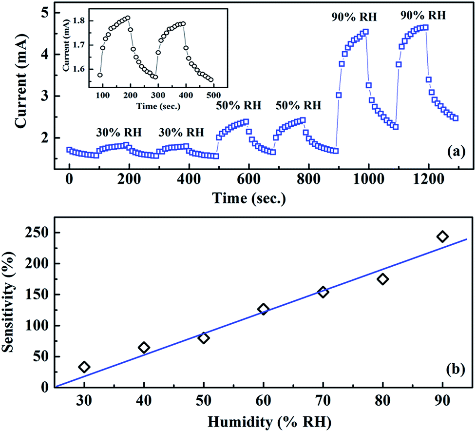 | ||
| Fig. 8 (a) Dynamic responses of the n-MoS2/p-Si junction upon consequent humidity at +4.0 V. The inset shows the enlarged image of the response to 30% RH. (b) Dependence of the sensing response of the junction on humidity levels. | ||
According to theoretical calculations, H2O molecules can be adsorbed on the surface of MoS2 due to the charge transfer between them.21 The interaction between the adsorbed gas molecules and underlying MoS2 is physisorption because of the small adsorption energy and large separation distance.22 Thus, fast response to humidity and recovery for MoS2-based materials could be realized. As shown in Fig. 3, the surface of the as-grown MoS2 film on Si is composed of cone-like grains. Large quantities of nanoscale grains could increase greatly the contact area of MoS2 to H2O molecules. Fig. 9(a) shows the schematic of the n-MoS2/p-Si junction under ambient humidity conditions. When the n-MoS2/p-Si junction is exposed to humidity gas, large numbers of H2O molecules can be adsorbed on the surface of MoS2 film. Subsequently, some of the adsorbed molecules could be capable of diffusing into the whole layer of the MoS2 film through the pores caused by grain boundaries at the surface (shown in Fig. 4), and even reach the interface area of the junction. As H2O is an electron donor,23 n-doping characteristics can be exhibited when H2O molecules are adsorbed on the MoS2 film. The Fermi level of the MoS2 film is shifted towards the conduction band. Because of the n-type nature of the as-grown MoS2 film, the carrier density of the film can be enhanced by the adsorbed H2O molecules. On the other hand, the energy barrier (eVbi) at MoS2/Si interface increases due to the movement of the Fermi level of the film. Thus, the electrical transporting properties of the MoS2/Si junction could be changed dramatically after H2O adsorption. According to the equivalent circuit model of the heterojunction for current measurements in Fig. 9. The current through the sample is determined mainly by the resistance of the MoS2 film (RMoS2), the barrier resistance (RBarrier) caused by the energy barrier at the interface and the resistance of the Si substrate (RSi), I = V/(RMoS2 + RBarrier + RSi). During our experiments, RSi is a constant and has not any change after the exposure to humidity condition. Thus, the response of the fabricated junction mainly originates from the effect of H2O adsorption on RMoS2 and RBarrier. Obviously, the adsorption has different effects on RMoS2 and RBarrier. After adsorption, RBarrier increases due to the increase of the interfacial barrier height, while RMoS2 decreases due to the increase of the electron concentration in the film. When a forward voltage is applied on the sample, the junction is biased positively and the conduction of the sample is dominated by the film. Thus, the response of the heterojunction with the increase of the forward current can be seen from Fig. 7(a). With increasing the forward voltage, the interfacial barrier height decreases gradually. This weakens the effect of RBarrier on the conduction of the p–n junction. Thus, the sensitivity increases with increasing the forward voltage, as shown in Fig. 7(b). After a threshold voltage (+1.9 V), the interfacial barrier vanishes and the conduction of the p–n junction is controlled completely by the MoS2 film. At this condition, the sensitivity becomes saturated and almost no change with further increasing the voltage, which is similar with that for the single MoS2 sensor devices.20 When a reverse voltage is applied, the junction is biased negatively and the interfacial barrier height increases. The charges near the interface are depleted and one depletion layer at the MoS2/Si interface can be formed. At this condition, the external voltage almost drops on the depletion layer and the conduction is controlled by RBarrier. Thus, the reverse current decreases when the dry-air conditions are changed into humidity conditions, as shown in Fig. 7. This is contrary to the current change in forward voltage range in the humidity condition. As shown in Fig. 4, the MoS2 film deposited at RT has much smaller pore size than the film deposited at 400 °C. Comparatively, it is more difficult for H2O molecules on the surface of the film deposited at RT to inject into the body. Thus, weak response to humidity gas can be seen in the junction with the MoS2 film deposited at RT, while strong response can be exhibited in the junction with the film deposited at 400 °C.
 | ||
| Fig. 9 Schematic of the n-MoS2/p-Si junction under humidity condition and the equivalent circuit model of the heterojunction for current measurements. | ||
When humidity conditions are changed into dry-air conditions, the adsorbed H2O molecules are desorbed easily from the MoS2 film due to their physisorption nature and small adsorption energies. As a result, the original electron concentration of MoS2 films is recovered and so is the junction current. Thus, the n-MoS2/p-Si junction exhibits humidity gas sensing properties, as shown in Fig. 8.
IV Conclusions
Bulk-like MoS2 thin films were grown on p-type Si substrates by dc magnetron sputtering technique and n-MoS2/p-Si junctions were fabricated. The fabricated junction exhibited obvious sensing properties to different humidity levels. In the forward voltage range, the currents increased significantly after the junction were exposed to humidity gas and the sensitivity increased with increasing voltage. The reverse current decreases under humidity conditions. An almost linear correlation was obtained in the measured range of humidity levels. This work demonstrates that n-MoS2/p-Si junctions have a large potential application in the area of humidity sensing.Acknowledgements
The authors would like to acknowledge the financial support by the Fundamental Research Funds for the Central Universities (14CX05038A, 15CX08009A and 15CX08010A) and the National Science Foundation of China (Grant No. 51502348, 51102284, 51372030 and 21476262).References
- B. Radisavljevic, A. Radenovi, J. Brivio, V. Giacometti and A. Kis, Nat. Nanotechnol., 2011, 6, 147 CrossRef CAS PubMed; C. Ataca, H. Sahin, E. Aktuörk and S. Ciraci, J. Phys. Chem. C, 2011, 115, 3934 Search PubMed; M. Bernardi, M. Palummo and J. C. Grossman, Nano Lett., 2013, 13, 3664 CrossRef PubMed.
- Y. Yoon, K. Ganapathi and S. Salahuddin, Nano Lett., 2011, 11, 3768 CrossRef CAS PubMed; R. Ganatra and Q. Zhang, ACS Nano, 2014, 8, 4074 CrossRef PubMed.
- K. Lee, R. Gatensby, N. McEvoy, T. Hallam and G. S. Duesberg, Adv. Mater., 2013, 25, 6699 CrossRef CAS PubMed; Y. Yao, L. Tolentino, Z. Yang, X. Song, W. Zhang, Y. Chen and C. Wong, Adv. Funct. Mater., 2013, 23, 3577 CrossRef PubMed.
- L. Hao, Y. Liu, W. Gao, Z. Han, Q. Xue, H. Zeng, Z. Wu, J. Zhu and W. Zhang, J. Appl. Phys., 2015, 117, 114502 CrossRef CAS PubMed; S. Wi, H. Kim, M. Chen, H. Nam, L. J. Guo, E. Meyhofer and X. Liang, ACS Nano, 2014, 8, 5270 CrossRef PubMed; K. Jiao, C. Duan, X. Wu, J. Chen, Y. Wang and Y. Chen, Phys. Chem. Chem. Phys., 2015, 17, 8182 RSC.
- S. L. Zhang, H. H. Choi, H. Y. Yue and W. C. Yang, Curr. Appl. Phys., 2014, 14, 264 CrossRef PubMed.
- X. Y. Feng, W. F. Chen and L. F. Yan, Sens. Actuators, B, 2015, 215, 316 CrossRef CAS PubMed.
- X. Gao, X. Zhang, C. Wan, X. Zhang, L. Wu and X. Tan, Appl. Phys. Lett., 2010, 97, 212101 CrossRef PubMed.
- K. Jiang, T. Fei and T. Zhang, RSC Adv., 2014, 4, 28451 RSC.
- H. Li, Z. Yin, Q. He, H. Li, X. Huang, G. Lu, D. Fam, A. Tok, Q. Zhang and H. Zhang, Small, 2012, 8, 63 CrossRef CAS PubMed; D. Sarkar, W. Liu, X. Xie, A. C. Anselmo, S. Mitragotri and K. Banerjee, ACS Nano, 2014, 8, 3992 CrossRef PubMed; F. K. Perkins, A. L. Friedman, E. Cobas, P. M. Campbell, G. G. Jernigan and B. T. Jonker, Nano Lett., 2013, 13, 668 CrossRef PubMed.
- L. Wang, J. Jie, Z. Shao, Q. Zhang, X. Zhang, Y. Wang, Z. Sun and S. T. Lee, Adv. Funct. Mater., 2015, 25, 2910 CrossRef CAS PubMed; M. R. Esmaeili-Rad and S. Salahuddin, Sci. Rep., 2013, 3, 2345 Search PubMed.
- Y. Liu, L. Hao, W. Gao, Z. Wu, Y. Lin, G. Li, W. Guo, L. Yu, H. Zeng, J. Zhu and W. Zhang, Sens. Actuators, B, 2015, 211, 537 CrossRef CAS PubMed; Y. Liu, L. Hao, W. Gao, Q. Xue, W. Guo, Z. Wu, Y. Lin, H. Zeng, J. Zhu and W. Zhang, J. Alloys Compd., 2015, 631, 105 CrossRef PubMed.
- D. R. Miller, S. A. Akbar and P. A. Morris, Sens. Actuators, B, 2014, 204, 250 CrossRef CAS PubMed; S. Bai, D. Li, D. Han, R. Luo, A. Chena and C. L. Chung, Sens. Actuators, B, 2010, 150, 749 CrossRef PubMed; M. Ivanovskaya, D. Kotsikau, G. Faglia and P. Nelli, Sens. Actuators, B, 2003, 96, 498 CrossRef.
- R. Ganatra and Q. Zhang, ACS Nano, 2014, 8, 4074 CrossRef CAS PubMed; Y. H. Lee, X. Q. Zhang, W. Zhang, M. T. Chang, C. T. Lin, K. D. Chang, Y. C. Yu, J. T. W. Wang, C. S. Chang, L. J. Li and T. W. Lin, Adv. Mater., 2012, 24, 2320 CrossRef PubMed.
- D. J. Late, P. A. Shaikh, R. Khare, R. V. Kashid, M. Chaudhary, M. A. More and S. B. Ogale, ACS Appl. Mater. Interfaces, 2014, 6, 15881 CAS.
- H. Huang, G. Fang, X. Mo, L. Yuan, H. Zhou, M. Wang, H. Xiao and X. Zhao, Appl. Phys. Lett., 2009, 94, 063512 CrossRef PubMed.
- L. Z. Hao, W. Gao, Y. J. Liu, Z. D. Han, Q. Z. Xue, W. Y. Guo, J. Zhu and Y. R. Li, Nanoscale, 2015, 7, 8304 RSC.
- S. M. Sze and K. K. Ng, Physics of Semiconductor Devices, 3rd edn, Wiley, New York, 2007 Search PubMed.
- D. A. Neamen, Semiconductor Physics and Devices: Basic Principles, McGraw-Hill, New York, 2003 Search PubMed.
- M. Fontana, T. Deppe, A. K. Boyd, M. Rinzan, A. Y. Liu, M. Paranjape and P. Barbara, Sci. Rep., 2013, 3, 1634 Search PubMed.
- X. Wang, S. Yang, Q. Yue, F. Wu and J. Li, J. Alloys Compd., 2014, 615, 989 CrossRef CAS PubMed.
- Q. Yue, Z. Shao, S. Chang and J. Li, Nanoscale Res. Lett., 2013, 8, 425 CrossRef PubMed.
- B. Cho, M. G. Hahm, M. Choi, J. Yoon, A. R. Kim, Y. J. Lee, S. G. Park, J. D. Kwon, C. S. Kim, M. Song, Y. Jeong, K. S. Nam, S. Lee, T. J. Yoo, C. G. Kang, B. H. Lee, H. C. Ko, P. M. Ajayan and D. H. Kim, Sci. Rep., 2015, 5, 8052 CrossRef CAS PubMed.
- D. J. Late, Y. K. Huang, B. Liu, J. Acharya, S. N. Shirodkar, J. Luo, A. Yan, D. Charles, U. V. Waghmare, V. P. Dravid and C. N. R. Rao, ACS Nano, 2013, 7, 4879 CrossRef CAS PubMed.
| This journal is © The Royal Society of Chemistry 2015 |