
Stable, highly conductive and orthogonal silver nanowire networks via zwitterionic treatment†
Hui
Li
a,
Qiaomei
Chen
*a,
Guangcong
Zhang
a,
Zhou
Zhang
a,
Jie
Fang
b,
Chaowei
Zhao
 b and
Weiwei
Li
*a
b and
Weiwei
Li
*a
aBeijing Advanced Innovation Center for Soft Matter Science and Engineering, State Key Laboratory of Organic–Inorganic Composites, Beijing University of Chemical Technology, Beijing 100029, P. R. China. E-mail: chenqm@mail.buct.edu.cn; liweiwei@iccas.ac.cn
bInstitute of Applied Chemistry, Jiangxi Academy of Sciences, Nanchang 330096, P. R. China
First published on 29th November 2022
Abstract
Silver nanowires (AgNWs) are the most important transparent electrodes for flexible optoelectronics. Their high aspect ratio and metallic nature make them tend to aggregate and yield inhomogeneous conducting films, which is detrimental to device performance. Here, a zwitterionic molecule was introduced into AgNW suspensions to tackle these drawbacks. The anionic part of the zwitterionic molecule absorbs on the surface of AgNWs, while the cations help the homogeneous dispersion of AgNWs in suspensions. More importantly, the cations generate electrostatic repulsion, which forces the AgNWs to form orthogonal networks with cut-off angles approaching 90°. These perfect AgNW networks showed superior photoelectric performance (with a sheet resistance of ∼11.8 Ω cm−2 and transmittance at 550 nm of ∼94.4%) and excellent storage stability. As a demonstration of their application, a flexible transparent electrode was fabricated via semi-embedding the AgNW networks in a polyimide substrate and applied to flexible organic solar cells, which exhibit superior mechanical stability (maintaining > 92% of the initial efficiency after 30![[thin space (1/6-em)]](https://www.rsc.org/images/entities/char_2009.gif) 000 bending cycles at a small radius of 1 mm). Therefore, stable, highly conductive and orthogonal AgNW networks can be obtained via zwitterionic treatment and show potential in flexible optoelectronics.
000 bending cycles at a small radius of 1 mm). Therefore, stable, highly conductive and orthogonal AgNW networks can be obtained via zwitterionic treatment and show potential in flexible optoelectronics.
1. Introduction
Flexible optoelectronic devices, such as organic field-effect transistors, photodetectors, and organic solar cells (OSCs), have attracted much attention in recent years due to their advantages of flexibility, light weight, compatibility with curved surfaces, low-cost roll-to-roll processing, etc.1–9 Flexible transparent electrodes (FTEs, including electrodes and flexible substrates) are the key components in these devices, which are responsible for transporting charges and maintaining mechanical stability under bending/twisting deformation. Silver nanowires (AgNWs) that can be dispersed into aqueous or alcoholic solution have been widely used as transparent electrodes in flexible optoelectronics due to their low resistance, high light transmission, flexibility and solution-processing.10 However, AgNWs also suffer from many drawbacks, such as high roughness, inferior interfacial adhesion, and poor storage stability. Besides, since AgNWs always have a high aspect ratio with a length of 5–100 μm and diameter of 10–200 nm, they tend to aggregate in both suspensions and film electrodes, degrading their overall photoelectric performance.11,12 These issues hamper the application of AgNWs in flexible optoelectronic devices.Researchers have been devoted to addressing the above issues of AgNW electrodes in these years. It has been proved that semi-embedding AgNWs into polymer substrates is an effective strategy to reduce the surface roughness, enhance interfacial adhesion and stability of AgNW electrodes.13–23 As with the photoelectric performance, researchers have mainly been involved in post-treatment of AgNW electrodes to reduce the contact resistance and improve the conductivity, which usually has little effect on enhancing the optical transmittance.11,12,23–28 According to the percolation theory,29,30 an orthogonal alignment of AgNWs (i.e., with cut-off angles approaching 90°) is the most effective strategy to balance the trade-off between the conductivity and optical transmittance, but this is very challenging to realize in solution-processed AgNW electrodes. Though the alignment of AgNWs has been realized through various techniques, such as the Langmuir–Blodgett technique,31 shear-induced alignment,32,33 capillary force-induced alignment,34 agitation-assisted assembly,35,36 and conical fiber array-guided alignment,37 these techniques still suffer from drawbacks such as complicated and time-consuming processes (substrate prepatterning, post-transfer, and pregrowing nanowires) and poor control at the microscopic scale, which will hinder their large-scale applications. In addition to the above techniques, introducing electrostatic repulsive force among AgNWs is another effective strategy to improve the dispersibility of nanowires both in the suspensions and during the film formation process. For example, Chen et al.38 proposed an ionic electrostatic repulsion strategy to reduce the aggregation of AgNWs via adding a polyelectrolyte into the AgNW suspension, realizing a grid-like AgNW FTE with excellent photoelectric performance and a smooth surface (with a roughness of ∼8.2 nm). Though great progress has been achieved by using this polyelectrolyte treatment, it is still necessary to further reduce the surface roughness, enhance the interfacial adhesion and stability of AgNW electrodes for practical applications. Considering the superiority of the semi-embedding strategy in terms of surface roughness (usually below 1 nm) and interfacial robustness, it is necessary to combine the semi-embedding and electrostatic repulsion strategies to obtain high-performance AgNW FTEs.
In this work, we develop a strategy to treat AgNWs in suspensions with a zwitterionic molecule, resulting in orthogonal AgNW networks with excellent photoelectric performance. Zwitterionic molecules consist of an equal number of oppositely charged cationic and anionic groups, where the cationic and anionic groups are separated by a short molecular chain.39,40 The zwitterionic molecule can absorb on the surface of AgNWs via electrostatic attraction between the anionic groups and Ag+. Thus, AgNW suspensions with a stable, homogeneous dispersion can be obtained owing to the strong hydration effects of zwitterions and electrostatic repulsion of cations, which also forces the AgNWs to form orthogonal networks with angles approaching 90° during the film formation process. The related AgNW electrode exhibits encouraging photoelectric properties (with a sheet resistance (Rsh) of ∼11.8 Ω cm−2 and transmittance at 550 nm (T550) of ∼94.4%) and superior storage stability. Utilizing the strategy of semi-embedding AgNWs in a polyimide (PI) substrate that we previously reported,20 an FTE with excellent photoelectric performance, smooth surfaces (a roughness of ∼0.56 nm) and high mechanical bending stability was fabricated. To demonstrate the feasibility of the FTE for flexible optoelectronic devices, a flexible organic solar cell (FOSC) was fabricated, which shows outstanding mechanical stability (maintaining above 92% of the initial efficiency after 30000 bending cycles at a small bending radius of 1 mm).
2. Results and discussion
2.1. Preparation and characterization of the zwitterionic molecule treated AgNW electrode
Our protocol to fabricate a zwitterionic molecule treated AgNW electrode is illustrated in Fig. 1a, where the zwitterionic molecule used was 3-(N,N-dimethylmyristylammonio)propanesulfonate (SB3-14) and the related electrode is denoted as SB3-14@AgNWs thereinafter (the preparation details and optimization of treatment conditions can be found in the Materials and methods section and ESI†). In short, firstly, the zwitterionic compound 3-(N,N-dimethylmyristylammonio)propanesulfonate (SB3-14) was added into the AgNW suspension, followed by stirring at room temperature to allow the reaction between SB3-14 and AgNWs to proceed. Secondly, the excess SB3-14 in the suspension was removed by repeated centrifugation washing. Next, SB3-14@AgNWs were redispersed in the dispersion liquid (deionized water and isopropanol, 4/1 in volume ratio) to the required concentration (2.5 mg mL−1). Finally, the SB3-14@AgNW electrode was fabricated from the obtained suspensions via spin-coating. It can be seen that SB3-14 carries separated local anionic and cationic charges simultaneously. It has been proved previously that active Ag+ exists on the surface of AgNWs.24,38,41 Therefore, when added into the AgNW suspensions, SB3-14 can absorb on the surface of AgNWs via electrostatic attraction between the anionic groups (–SO3−) and Ag+, resulting in stable, homogeneous AgNW suspensions and AgNW electrodes with orthogonal patterns owing to the strong hydration effects of zwitterions and cationic electrostatic repulsion among the AgNWs during the film formation process. The zeta potentials of the untreated AgNWs and SB3-14@AgNWs in solution show little difference with zeta potentials of −7.8 mV and −6.4 mV (Fig. S1†), respectively, which further indicates that the bulk AgNWs are positively charged with Ag+. It is easy to explain the nearly unchanged zeta potential after the SB3-14 treatment, since zwitterions carry a net charge of zero at neutral pH. In order to further understand the electronic influence of SB3-14 treatment on AgNWs, 2D mapping of the surface potentials of the untreated AgNWs and SB3-14@AgNW surface (1 μm × 1 μm) was performed via kelvin probe force microscopy (KPFM) referenced to a Pt/Ir-coated Si tip. As shown in Fig. S2,† the potential difference between the surface and the probe was 157 mV for the untreated AgNWs and 238 mV for SB3-14@AgNWs, indicating that the surface potential was enhanced via SB3-14 treatment, which should be closely related to the introduced quaternary amine cations and justifies the above-stated mechanism of cationic electrostatic repulsion. | ||
| Fig. 1 (a) Schematic illustration for the preparation of the SB3-14@AgNW electrode. (b) Raman spectra of SB3-14@AgNWs and untreated AgNWs. Core-level XPS spectra of Ag 3d (c), S 2p (d), N 1s (e), and O 1s (f). | ||
Since the treatment conditions, such as the SB3-14 concentration and time, would affect the performance of the SB3-14@AgNW electrode, we investigated the effect of the molar ratio of SB3-14:Ag and treatment time on the Rsh of the related electrodes by the variable-controlling approach, where the treatment time (4 h) and molar ratio (4:1) were two constants, respectively. As shown in Fig. S3a,† as the molar ratio increases, the Rsh decreases gradually (with an average Rsh of 17.2 ± 3.1 Ω cm−2 for the untreated AgNW electrode), but it reached a plateau when the molar ratio is above 4:1, meaning that adding more SB3-14 makes no significant contribution. The treatment time has a similar trend of influence on the Rsh of electrodes, which approaches a plateau at treatment times above 1 h (Fig. S3b†). Based on the above investigations, SB3-14@AgNW electrodes in the following were prepared via treating for 4 h (to ensure sufficient modification) with a molar ratio of 4:1 and the Rsh value of the SB3-14@AgNW electrode on a glass substrate is 11.8 ± 0.97 Ω cm−2. The reason for the decreased Rsh after SB3-14 treatment will be discussed further below.
To confirm the successful modification of SB3-14 on the surface of AgNWs, Raman spectroscopy was conducted first. As shown in the Raman spectra (Fig. 1b), new bands at ∼1132 cm−1 and ∼1184 cm−1 ascribed to the bending vibration and asymmetric stretching of –SO3− appear in the SB3-14@AgNW Raman spectrum, which preliminarily confirms the successful absorption of SB3-14 on the surfaces of AgNWs.42,43 Besides, the band at ∼1765 cm−1 arising from carbonyl groups of polyvinyl pyrrolidone (PVP) on the surface of the untreated AgNWs can also be found in SB3-14@AgNWs, revealing that PVP still exists after SB3-14 treatment. Furthermore, X-ray photoelectron spectroscopy (XPS) deconvolution analysis was further carried out to study the molecular interactions between SB3-14 and Ag+ by analyzing shifts of the binding energy (BE) in the XPS spectra, where all of the BE values were calibrated by using a C 1s photoelectron BE value of 284.8 eV. The Ag 3d XPS core-level spectra in Fig. 1c show that when treated with SB3-14, the binding energy (BE) values of Ag 3d in SB3-14@AgNWs shift to lower values (by ∼0.5 eV), indicating the electrostatic attraction and charge transfer between the anionic groups (–SO3−) of SB3-14 and Ag+.44 Additionally, the S 2p (Fig. 1d), N 1s (Fig. 1e) and O 1s (Fig. 1f) core-level XPS deconvolution analysis confirmed the existence of SB3-14 on the surface of SB3-14@AgNWs. It can also be seen in the N 1s and O 1s core-level spectra that PVP still exists after SB3-14 treatment. Moreover, the BE values of N 1s and O 1s peaks arose from PVP and remained unchanged before and after SB3-14 treatment, indicating that there is no electrostatic attraction between PVP and SB3-14. Thus, if SB3-14 was simply attached to the surface of PVP, it will be easily washed off during the repeated centrifugation/redispersion treatment process. All above discussions indicated that SB3-14 interacts with AgNWs via electrostatic attraction between the anionic groups and Ag+, instead of being simply attached to the surface of PVP. The existence of PVP after SB3-14 treatment was further confirmed by the transmission electron microscopy (TEM) analysis. As shown in Fig. S4,† a thin layer coating of PVP (∼2–4 nm thickness) with a lighter contrast can be clearly seen on the edge of both SB3-14@AgNWs and untreated AgNWs with no noticeable difference. Therefore, we speculate that the modification mechanism is that SB3-14 absorbs at the position uncovered with PVP, resulting in a denser protective layer on the surface of SB3-14@AgNWs over the untreated AgNWs.
To get a deeper insight into the significantly reduced Rsh of the SB3-14@AgNW electrode by SB3-14 treatment, a scanning electron microscope (SEM) was first adopted to investigate the surface morphology of the SB3-14@AgNW and untreated AgNW electrodes, which were processed under the totally same conditions to ensure a parallel comparison. According to the percolation theory,29,30 an ideal trade-off between Rsh and optical transmittance can be achieved when AgNWs are orthogonally aligned (the crossed nanowires tend to be perpendicular to each other, i.e. the cut-off angle θ = 90°), which also requires a uniform distribution of AgNWs without aggregation. As shown in the SEM images (Fig. 2a), the SB3-14@AgNW electrode (I, II and III) shows a surface morphology with an uniform distribution in a grid-like pattern, while obvious aggregation (as the red circle marked in Fig. 2a, IV) can be observed in the untreated AgNW electrode (IV, V and VI) and the electrode shows a quite inhomogeneous distribution of AgNWs (the nanowires are closely packed at one position and loosely packed at another position). Further statistical analysis of AgNW coverages, hole areas (i.e., uncovered areas) and cut-off angles θ of the corresponding film electrodes was obtained from the SEM images (calculated using the ImageJ software). As summarized in Fig. S5,† the SB3-14@AgNW electrode shows a higher coverage (average of all the corresponding SEM images in Fig. 2a) of 33.6% than the untreated AgNW electrode (22.4%). Besides, compared with the SB3-14@AgNW electrode (with an average hole area of 0.028 ± 0.025 μm2, calculated from Fig. 2a, II), larger and inhomogeneous hole areas exist in the untreated AgNW electrode, with an average hole area of 0.063 ± 0.069 μm2 (calculated from Fig. 2a, V). Considering the same processing conditions of the two types of electrodes, the lower coverage and inhomogeneous hole areas may be ascribed to the aggregation of nanowires in the untreated AgNW electrode. Moreover, the average θ value is 74.3 ± 13.6° (calculated from Fig. 2a, II) for the SB3-14@AgNW electrode, compared with 56.4 ± 19.0° (calculated from Fig. 2a, V) for the untreated AgNW electrode. It should be pointed out that though the θ value of ∼74.3° is lower than the ideal value of 90° discussed above, it has been proved previously that the percolation threshold does not change substantially when the cut-off angle is in the range of 70–90°.38 The homogeneous distribution of SB3-14@AgNWs without aggregation and larger θ values synergistically lead to a relatively low Rsh value (11.8 ± 0.97 Ω cm−2).
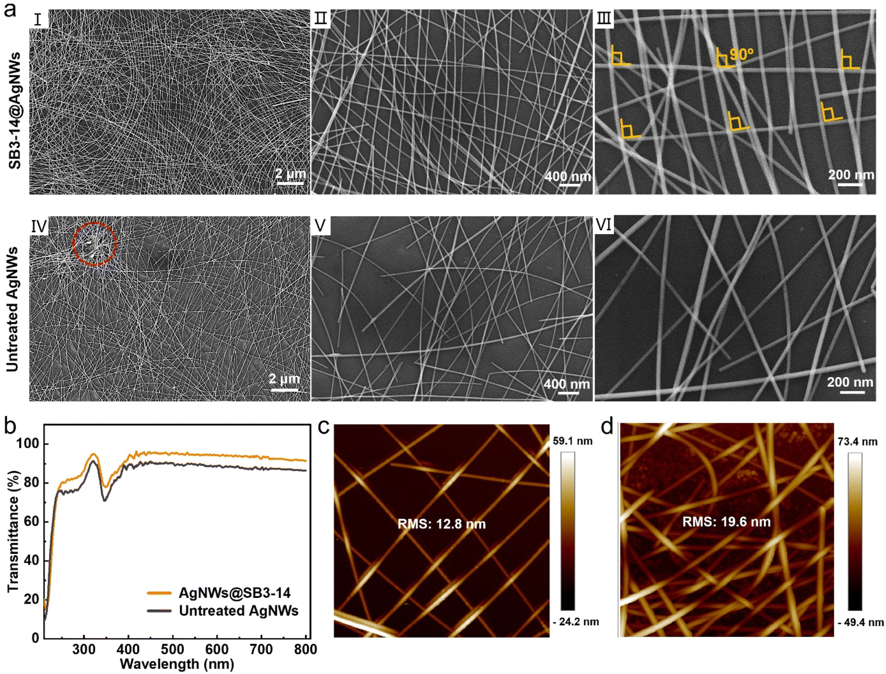 | ||
| Fig. 2 Characterization of the corresponding two types of electrodes. (a) SEM images of the SB3-14@AgNW electrode (I, II and III) and the untreated AgNW electrode (IV, V and VI), where the red circle in image IV shows obvious aggregation of nanowires. (b) Optical transmittance curves. AFM height images of the SB3-14@AgNW electrode (c) and untreated AgNW electrode (d). | ||
Next, the optical transmittance was investigated via the UV-vis transmittance tests. As shown in Fig. 2b, the untreated AgNW electrode exhibits an inferior T550 of about 89.7% than the SB3-14@AgNW electrode (∼94.4%), the reason for which may be ascribed to the aggregation of the untreated AgNWs as described above. To make this speculation more convincing, the atomic force microscopy (AFM) analysis was carried out. As shown in Fig. 2c and d, the SB3-14@AgNW electrode displays an orthogonal alignment and homogeneous distribution of nanowires while the untreated AgNW electrode shows a tanglesome distribution, in accordance with the SEM results in Fig. 2a. The root-mean-square roughness (RMS) of SB3-14@AgNWs and untreated AgNW electrodes are 12.8 nm and 19.6 nm, respectively, which further justifies the more homogeneous distribution of nanowires in the SB3-14@AgNW electrode. Additionally, SEM was conducted on the larger characterization area (100 × 60 μm2) of the two types of electrodes and three different positions of the same electrode were investigated to prove the generality of the nanowire distribution. It can be seen from the results that all three positions of the SB3-14@AgNW electrode (Fig. S6†) show a homogeneous distribution of nanowires while obvious and large aggregations are exhibited in all three positions of the untreated AgNW electrode (Fig. S7†). Thus the figure of merit (FoM, a critical parameter often used to quantitatively evaluate the trade-off between the Rsh and transmittance of transparent electrodes) of the SB3-14@AgNW and untreated AgNW electrodes (excluding the substrate) can be calculated to be 546 and 196, respectively,24,38 indicating the superior photoelectric performance of the SB3-14@AgNW electrode to the untreated AgNW electrode. The FoM was calculated from the ratio of direct-current conductivity (σDC) to optical conductivity (σOP(λ)) in eqn (1),
 | (1) |
2.2. Long-term stability of the SB3-14@AgNW electrode
In addition to the photoelectric performance, the long-term stability of AgNW electrodes is another critical issue for practical applications because AgNWs are susceptible to degradation in ambient environments.45,46 As stated earlier, the absorption of SB3-14 could form a more dense protective layer on the surface of AgNWs over the untreated ones, which could prevent AgNWs from corrosion. On the other hand, by saturating the surface of AgNWs with –SO3− groups, the formation of extra Ag2O/Ag2S could be avoided as every surface atom of silver would already be bonded. Therefore, the SB3-14@AgNW electrode is expected to be more stable than the untreated AgNW electrode. To verify the above speculation, the SB3-14@AgNW electrode was stored under the ambient atmosphere of the laboratory (average relative humidity, ∼50%; average temperature, ∼22 °C, in the dark) for 2 months, with the untreated AgNW electrode as a comparison. Fig. 3a and b show the Rsh change and ratio of conductive points for the two types of electrodes (statistical analysis of 15 different points from 3 individual electrodes) within 2 months. It can be found that the Rsh for both the SB3-14@AgNW electrode and untreated AgNW electrode increased slightly within 1 month of explosion and all the points remain conductive. After 2 months, the Rsh of the untreated AgNW electrode increased to 1.95 times (33.5 Ω cm−2) of its original value and some points became non-conducting (∼33%), while the SB3-14@AgNW electrode still shows a relatively low Rsh of 14.3 Ω cm−2 (increased only by ∼21%) and all the measured points reserve conductivity. Besides, SEM analysis (Fig. 3c) shows that many tiny nanoparticles and visible breaks form on the surface of the untreated AgNW electrode, which can explain the degradation and heterogeneity of its conducting properties. In contrast, the morphology of the SB3-14@AgNW electrode was unchanged. Furthermore, XPS deconvolution analysis was conducted to investigate the components of the tiny nanoparticles (Fig. 3d). Compared with the Ag 3d XPS core-level spectrum of the freshly untreated AgNW electrode, a silver oxide signature appears after storage for 2 months, while no sign of oxidation can be detected in the SB3-14@AgNW electrode after storage for the same period. All the results indicate the superior storage stability of the SB3-14@AgNW electrode over the untreated AgNW electrode. | ||
| Fig. 3 Long-term stability of the SB3-14@AgNW and untreated AgNW electrodes. (a) Sheet resistance (b) and the ratio of conductive point variation for the two types of electrodes stored for 2 months. (c) SEM images of the untreated AgNW and SB3-14@AgNW electrodes after being stored for 2 months. (d) XPS deconvolution analysis on the fresh and stored electrodes. | ||
2.3. Fabrication and performance of the FTE and FOSC
Based on the SB3-14@AgNW electrode, an FTE (thickness of ∼20 μm, denoted as Em-AgNW FTE) was constructed using the strategy of semi-embedding AgNWs in a polyimide (PI) substrate that we reported previously20 (the preparation details of the FTE can be found in the Materials and methods section). The UV-vis curves (Fig. S8†) show that the FTE possesses a high T550 value of about 88.3% (decreased slightly from 90.4% of the PI substrate), which is higher than that of similar FTEs in our previous studies.19–22 To justify the effectiveness of the semi-embedding strategy on reducing the surface roughness of AgNW electrodes, the AFM analysis was carried out. Fig. S9† shows the planar AFM image and height values obtained from the dashed line. The RMS of the investigated area is about 0.56 nm, which reveals that AgNWs have been well embedded in the PI substrate since the RMS value is much lower than the average diameter of AgNWs (∼25 nm). Moreover, since mechanical robustness of the FTE plays a significant role in operational stability of flexible optoelectronic devices, the mechanical stability of the Em-AgNW FTE was investigated via repeated bending tests at different radii (from 5 mm to 0 mm, as illustrated in the inset of Fig. 4a), which indicated that nearly no change for the Rsh could be observed after 1000 bending cycles at different radii, even when it was folded (i.e., at a bending radius of 0 mm). AFM analysis was conducted on the Em-AgNW FTE before and after bending at a radius of 0 mm for 1000 cycles. It can be seen from Fig. S10† that the surface morphology and RMS values show no obvious change. All results above indicate the great potential of the FTE for high-performance flexible optoelectronic devices. | ||
| Fig. 4 Performance of the Em-AgNW FTE and related FOSC. (a) The normalized Rsh of the Em-AgNW FTE after 1000 bending tests at different radii. (b) Structure illustration of the FOSC and chemical structures of PM6 and L8-BO. (c) J–V characteristic curves of the flexible and rigid devices. The normalized PCE values of the FOSC after 1000 bending cycles at different bending radii (d) and for cycles up to 30000 times at a radius of 1 mm (e). | ||
With the above attractive features, the FTE was applied to a FOSC device with the configuration of Em-AgNW FTE/ZnO/PM6:L8-BO/MoO3/Ag (Fig. 4b, the fabrication details can be found in the Materials and methods section) to prove its potential applications in flexible optoelectronic devices. Fig. 4c shows the current density–voltage (J–V) characteristic curves of the optimal FOSC and its rigid counterpart device based on ITO/glass (the corresponding photovoltaic parameters are summarized in Table S1†). The FOSC shows an optimal PCE of 15.41% with an open-circuit voltage (Voc) of 0.834 V, a short-circuit current density (Jsc) of 24.26 mA cm−2 and a fill factor (FF) of 76.34%. The rigid OSC provided a relatively higher PCE of 16.58%, particularly with a higher Voc of 0.879 V and Jsc of 25.34 mA cm−2. To investigate the Jsc deviation, the external quantum efficiency (EQE) spectral analysis was conducted on both the flexible and rigid OSC devices. As shown in Fig. S11 and Table S1,† the integrated Jsc values of the flexible and rigid OSC devices are 23.23 mA cm−2 and 24.17 mA cm−2, respectively, agreeing well with the Jsc values from the J–V characteristics with a deviation less than 5%. The J–V characteristics in the dark (shown in Fig. 4c) were also obtained to understand the device physics and the loss mechanisms, from which, the shunt resistance (Rsh) and series resistance (Rs) were obtained using the previously reported method (Fig. S12†).47,48 It can be seen that the FOSC shows a higher Rs than the rigid OSC, which may be ascribed to the relatively low conductivity of the Em-AgNW FTE (Rsh of the FTE and ITO are about 11.8 Ω sq−1 and 6.6 Ω sq−1, respectively) and the not ideal wettability of the ZnO ETLs upon the Em-AgNW FTE. Meanwhile, the lower Rsh of the FOSC than the rigid OSC may have arisen from the relatively larger leakage current density in the FOSC device.
Then mechanical stability of the FOSC was further investigated, which is another essential requirement for FOSCs because mechanical strain is unavoidable in practical applications. The mechanical robustness of the FOSC was first investigated via repeatedly bending the devices at various radii for 1000 times as illustrated in the inset of Fig. 4d. It can be seen from Fig. 4d that the average PCE (from 3 individual devices) of the FOSC maintains constant at radii from 5 mm to 1 mm and only declines by less than 2% when folding the devices (i.e., at a radius of 0 mm). We further conducted the bending tests at a fixed radius of 1 mm up to 30000 cycles. As shown in Fig. 4e, the PCE decreases gradually but still reserves >92% of the initial value. All the results above underline the superior mechanical robustness of the FOSC devices.
3. Conclusion
In conclusion, an AgNW electrode with superior photoelectric performance has been successfully fabricated via treating AgNWs in suspensions using a zwitterionic molecule SB3-14. The anions and cations function separately to absorb on the surface of AgNWs via electrostatic attraction between the –SO3− anionic groups and Ag+ and enhance electrostatic repulsion among AgNWs via quaternary amine groups, respectively. Thus, homogeneous AgNW suspensions and AgNW electrode with orthogonal patterns with encouraging photoelectric properties (Rsh of ∼11.8 Ω cm−2 and T550 of ∼94.4%) and excellent storage stability were obtained. An FTE with excellent photoelectric performance, smooth surfaces and high mechanical robustness was fabricated via semi-embedding AgNWs in a PI substrate. Based on this FTE, an FOSC device with a PCE of 15.41% and outstanding mechanical stability (reserving >92% of the initial PCE after 30000 bending cycles at a small bending radius of 1 mm) was constructed. This work offers an effective and universal platform to fabricate high-performance FTEs for flexible optoelectronic devices.
4. Materials and methods
4.1. Materials
3-(N,N-Dimethylmyristylammonio)propanesulfonate (SB3-14, 98%), 2-mercaptoethanesulfonate (98%), 6-mercapto-1-hexanol (97%), 11-mercaptoundecanoic acid (95%), zinc acetate dihydrate and ethanolamine were purchased from Acros and directly used without any purification. Isopropyl alcohol (IPA, AR), N,N-dimethylacetamide (DMAc, AR) and 2-methoxyethanol (AR) were purchased from Damao Chemical Reagent Factory, Tian Jing, China. The original AgNW dispersions in water (10 mg mL−1, with an average length of 10–30 μm and diameter of 20–30 nm) were purchased from Zhejiang Kechaung Advanced Materials Co., Ltd. PM6 was provided by Solarmer Materials Inc. L8-BO was purchased from Organtec Ltd. 1,3-Dibromo-5-chlorobenzene (DBCL, 98%) was purchased from TCI. PFNDI-Br was purchased from eFlexPV Limited. Silver slug (99.999%) and molybdenum oxide (99.9%) for evaporation were offered by Alfa Aesar. Glass/ITO and glass were purchased from South Chain Science & Technology Company Limited.4.2. General measurements
Raman spectra were recorded using a LabRAM HR Evolution spectrometer (HORIBA Jobin Yvon). X-ray photoelectron spectroscopy (XPS) was conducted on a Thermo Scientific K-Alpha photoelectron spectroscopy, where all of the BE values were calibrated by using a C 1s photoelectron BE value of 284.8 eV. The surface morphologies were investigated using a Zeiss Gemini 300 field-emission scanning electron microscope (SEM). Transmission electron microscopy (TEM) was performed on a FEI Talos F200S spectrometer. The roughness of the embedded AgNW FTE was measured using an atomic force microscope (AFM, Bruker Dimension Icon). The surface potential measurements were conducted in air via kelvin probe force microscopy (KPFM) with a Bruker Dimension Icon AFM equipped with a MAC III controller (providing three lock-in amplifiers) using a Pt/Ir-coated Si tip (PPP-EFM-10, nanosensors). The zeta potential measurements were performed using an NS-90Z zeta potential analyzer. Optical transmittance spectra were recorded using a UV-vis-NIR spectrophotometer (UV-3900H) in the wavelength range from 200 nm to 800 nm. The sheet resistance of the electrodes (average value of 15 different points from 3 individual electrodes) was measured using an ST-300 multifunction digital four-probe tester. The current density–voltage (J–V) curves of OSC devices were recorded inside a N2-filled glove box under AM1.5G (100 mW cm−2) illumination from a solar simulator (Enlitech model SS-F5-3A) with a standard silicon solar cell equipped with a KG5 filter (certificated by the National Institute of Metrology) and a Keithley 2400 source-measure unit. The active area of the cells was defined to be 0.0289 cm2 using a shadow mask. The external quantum efficiency (EQE) spectra were measured with a QE-R Solar Cell Spectral Response Measurement System (Enlitech).4.3. Preparation of the SB3-14@AgNW suspensions
The SB3-14@AgNW suspensions in this work were prepared according to the following procedure. SB3-14 (2 mol) was completely dissolved in deionized water (1 mL). The original AgNW suspensions (10 mg mL−1) were diluted with deionized water and IPA (4/1, v/v) to 5 mg mL−1. Then, the SB3-14 solution was added to the diluted AgNW dispersions under stirring (1000 rpm), where the molar ratio of SB3-14/Ag was 4/1. The solution mixture was left to react for another 4 h under mild stirring (400 rpm), followed by washing twice by centrifugation (5000 rpm, 8 min) and redispersed in the same volume of water and IPA (4/1, v/v). The accurate concentration of the resulting SB3-14@AgNW suspensions was confirmed by evaporating the solvent with heat. Finally, the suspensions were diluted to 2.5 mg mL−1 for use.4.4. Fabrication of the SB3-14@AgNW electrode, untreated AgNW electrode and Em-AgNW FTE
First, the glass substrates were cleaned by sequential ultrasonic treatments with detergent, deionized water, acetone, and IPA for 10 min, followed by Ar plasma treatment for 2 min. Next, the above SB3-14@AgNW suspension (2.5 mg mL−1) was spin-coated (1200 rpm for 40 s) on the cleaned glass substrates and annealed at 100 °C for 10 min, which was repeated one more time, obtaining the SB3-14@AgNW electrode. The untreated AgNW electrode was prepared via the same way as the SB3-14@AgNW electrode, where the only difference was that the untreated AgNW suspension was utilized. The above SB3-14@AgNW films were patterned by solvent wiping to certain shapes. Then the polyimide (PI) solid particles, synthesized according to our previous work,20 were dissolved in DMAc with a solid content of 5 wt% and stirred at room temperature to obtain a homogeneous viscous solution. Next, the solution was transferred to the patterned SB3-14@AgNW electrodes via droplet coating and step-wise annealed from 30 to 180 °C with an increase of 30 °C and holding for 30 min at each step. At last, the Em-AgNW FTE was obtained by peeling off from the glass substrate with the aid of water.4.5. Fabrication of the flexible and rigid OSC devices
The following gives fabrication details of the flexible organic solar cell (FOSC) devices. Firstly, the polydimethylsiloxane (PDMS) films were prepared by spin-coating the mixture of the polymeric base and curing agent (20/1, v/v, SYLGARD 184, Dow Corning Inc.) on the cleaned glass substrates at 3000 rpm for 30 s, followed by curing at 100 °C for 5 min. The Em-AgNW FTEs were attached to the cleaned glass substrates by using PDMS as the adhesive film and treated with Ar plasma for 2 min to improve the surface wettability. Then, the ZnO sol–gel precursor solution was spin-coated on the Em-AgNW FTEs (3000 rpm, 40 s) and annealed at 150 °C for 15 min to form the electron transporting layer (ETL), where the precursor solution was prepared by dissolving 0.1 g zinc acetate dihydrate and 28.9 μL ethanolamine in 0.935 mL 2-methoxyethanol and stirring overnight. Thirdly, the Em-AgNW FTEs with ZnO layers were transferred into a N2-filled glove box. The PM6:L8-BO (weight ratio of 1:1.2, 16 mg mL−1 in chloroform with 12 mg mL−1 DBCL as the additive) blend was then spin-coated at a speed of 3200 rpm for 40 s to form a ∼100 nm photoactive layer. Finally, molybdenum oxide (MoO3, 10 nm) and silver slug (Ag, 80 nm) were thermally deposited onto the photoactive layer to form the hole transporting layer (HTL) and top electrode.
The rigid OSC devices were constructed in a similar way to the FOSC by replacing the Em-AgNW FTEs with clean ITO/glass.
Conflicts of interest
There are no conflicts to declare.Acknowledgements
This study was jointly supported by the National Natural Science Foundation of China (No. 21905158, 52073016 and 92163128) and Beijing Natural Science Foundation (No. 2212045 and JQ21006). This work was further supported by the Fundamental Research Funds for the Central Universities (No. buctrc202111, buctrc201828 and XK1802-2), the Opening Foundation of State Key Laboratory of Organic–Inorganic Composites of Beijing University of Chemical Technology (No. oic-202201006) and Jiangxi Provincial Department of Science and Technology (No. 20202ACBL213004, 20212BCJ23035, and jxsq2019102004).References
- S. Huang, Y. Liu, Y. Zhao, Z. Ren and C. F. Guo, Adv. Funct. Mater., 2018, 29, 1805924 CrossRef.
- T. Someya and M. Amagai, Nat. Biotechnol., 2019, 37, 382–388 CrossRef CAS PubMed.
- K. Fukuda, K. Yu and T. Someya, Adv. Energy Mater., 2020, 2000765 CrossRef CAS.
- K. Schlingman, Y. Chen, R. S. Carmichael and T. B. Carmichael, Adv. Mater., 2021, e2006863 CrossRef PubMed.
- K. Fukuda, K. Yu and T. Someya, Adv. Energy Mater., 2020, 10, 2000765 CrossRef CAS.
- J. Qin, L. Lan, S. Chen, F. Huang, H. Shi, W. Chen, H. Xia, K. Sun and C. Yang, Adv. Funct. Mater., 2020, 30, 2002529 CrossRef CAS.
- C. Liu, C. Xiao, C. Xie and W. Li, Nano Energy, 2021, 89, 106399 CrossRef CAS.
- J. Xu, T. Peng, X. Qin, Q. Zhang, T. Liu, W. Dai, B. Chen, H. Yu and S. Shi, J. Mater. Chem. A, 2021, 9, 14147–14171 RSC.
- W. Li, H. Zhang, S. Shi, J. Xu, X. Qin, Q. He, K. Yang, W. Dai, G. Liu, Q. Zhou, H. Yu, S. R. P. Silva and M. Fahlman, J. Mater. Chem. C, 2020, 8, 4636–4674 RSC.
- M. R. Azani, A. Hassanpour and T. Torres, Adv. Energy Mater., 2020, 10, 2002536 CrossRef CAS.
- G. Xu and Y. Li, Nano Sel., 2020, 1, 169–182 CrossRef.
- V. H. Nguyen, D. T. Papanastasiou, J. Resende, L. Bardet, T. Sannicolo, C. Jimenez, D. Munoz-Rojas, N. D. Nguyen and D. Bellet, Small, 2022, 18, e2106006 CrossRef PubMed.
- D. Chen, J. Liang, C. Liu, G. Saldanha, F. Zhao, K. Tong, J. Liu and Q. Pei, Adv. Funct. Mater., 2015, 25, 7512–7520 CrossRef.
- J. A. Spechler, T.-W. Koh, J. T. Herb, B. P. Rand and C. B. Arnold, Adv. Funct. Mater., 2015, 25, 7428–7434 CrossRef.
- X. Dong, P. Shi, L. Sun, J. Li, F. Qin, S. Xiong, T. Liu, X. Jiang and Y. Zhou, J. Mater. Chem. A, 2019, 7, 1989–1995 RSC.
- D. T. Nguyen and H. Youn, ACS Appl. Mater. Interfaces, 2019, 11, 42469–42478 CrossRef CAS PubMed.
- L. Sun, W. Zeng, C. Xie, L. Hu, X. Dong, F. Qin, W. Wang, T. Liu, X. Jiang, Y. Jiang and Y. Zhou, Adv. Mater., 2020, 32, e1907840 CrossRef PubMed.
- X. Yin, J. Wang, A. Liu, W. Cai, L. Ying, X. He, Z. Tang and L. Hou, Flexible Printed Electron., 2020, 5, 014003 CrossRef CAS.
- Y. Wang, Q. Chen, Y. Wang, G. Zhang, Z. Zhang, J. Fang, C. Zhao and W. Li, Macromol. Rapid Commun., 2022, e2200432 CrossRef PubMed.
- Y. Wang, Q. Chen, G. Zhang, C. Xiao, Y. Wei and W. Li, ACS Appl. Mater. Interfaces, 2022, 14, 5699–5708 CrossRef CAS PubMed.
- G. Zhang, Q. Chen, C. Xie, Y. Wang, C. Zhao, C. Xiao, Y. Wei and W. Li, npj Flexible Electron., 2022, 6, 37 CrossRef CAS.
- Y. Wang, Q. Chen, G. Zhang, Y. Wang, Z. Zhang, J. Fang, C. Zhao and W. Li, Chem. Eng. J., 2023, 451, 138612 CrossRef CAS.
- J. Kim, D. Ouyang, H. Lu, F. Ye, Y. Guo, N. Zhao and W. C. H. Choy, Adv. Energy Mater., 2020, 10, 1903919 CrossRef CAS.
- G. Zeng, W. Chen, X. Chen, Y. Hu, Y. Chen, B. Zhang, H. Chen, W. Sun, Y. Shen, Y. Li, F. Yan and Y. Li, J. Am. Chem. Soc., 2022, 144, 8658–8668 CrossRef CAS PubMed.
- X. Chu, K. Wang, J. Tao, S. Li, S. Ji and C. Ye, Nanomaterials, 2019, 9, 533 CrossRef PubMed.
- A. Madeira, M. Plissonneau, L. Servant, I. A. Goldthorpe and M. Treguer-Delapierre, Nanomaterials, 2019, 9, 899 CrossRef CAS PubMed.
- Y. Ge, X. Duan, M. Zhang, L. Mei, J. Hu, W. Hu and X. Duan, J. Am. Chem. Soc., 2018, 140, 193–199 CrossRef CAS PubMed.
- G. S. Liu, Y. Xu, Y. Kong, L. Wang, J. Wang, X. Xie, Y. Luo and B. R. Yang, ACS Appl. Mater. Interfaces, 2018, 10, 37699–37708 CrossRef CAS PubMed.
- S. De and J. N. Coleman, MRS Bull., 2011, 36, 774–781 CrossRef CAS.
- I. Balberg and N. Binenbaum, Phys. Rev. B: Condens. Matter Mater. Phys., 1983, 28, 3799–3812 CrossRef.
- J. L. Wang, Y. R. Lu, H. H. Li, J. W. Liu and S. H. Yu, J. Am. Chem. Soc., 2017, 139, 9921–9926 CrossRef CAS PubMed.
- S. Cho, S. Kang, A. Pandya, R. Shanker, Z. Khan, Y. Lee, J. Park, S. L. Craig and H. Ko, ACS Nano, 2017, 11, 4346–4357 CrossRef CAS PubMed.
- Y. Ko, S. K. Song, N. H. Kim and S. T. Chang, Langmuir, 2016, 32, 366–373 CrossRef CAS PubMed.
- S. Kang, T. Kim, S. Cho, Y. Lee, A. Choe, B. Walker, S. J. Ko, J. Y. Kim and H. Ko, Nano Lett., 2015, 15, 7933–7942 CrossRef CAS PubMed.
- H. Hu, S. Wang, S. Wang, G. Liu, T. Cao and Y. Long, Adv. Funct. Mater., 2019, 29, 1902922 CrossRef.
- H. Hu, S. Wang, Y. Meng, G. Liu, M. Li, T. D. Vu and Y. Long, Adv. Mater. Technol., 2022, 7, 2100824 CrossRef CAS.
- L. Meng, M. Zhang, H. Deng, B. Xu, H. Wang, Y. Wang, L. Jiang and H. Liu, CCS Chem., 2021, 3, 2194–2202 CrossRef CAS.
- Y. Sun, M. Chang, L. Meng, X. Wan, H. Gao, Y. Zhang, K. Zhao, Z. Sun, C. Li, S. Liu, H. Wang, J. Liang and Y. Chen, Nat. Electron., 2019, 2, 513–520 CrossRef CAS.
- A. Erfani, J. Seaberg, C. P. Aichele and J. D. Ramsey, Biomacromolecules, 2020, 21, 2557–2573 CrossRef CAS PubMed.
- L. D. Blackman, P. A. Gunatillake, P. Cass and K. E. S. Locock, Chem. Soc. Rev., 2019, 48, 757–770 RSC.
- Y. Zhao, X. Wang, S. Yang, E. Kuttner, A. A. Taylor, R. Salemmilani, X. Liu, M. Moskovits, B. Wu, A. Dehestani, J. F. Li, M. F. Chisholm, Z. Q. Tian, F. R. Fan, J. Jiang and G. D. Stucky, J. Am. Chem. Soc., 2019, 141, 13977–13986 CrossRef CAS PubMed.
- C. Y. Panicker, H. T. Varghese, D. Philip and H. I. Nogueira, Spectrochim. Acta, Part A, 2006, 64, 744–747 CrossRef PubMed.
- C.-W. Chu, Y. Higaki, C.-H. Cheng, M.-H. Cheng, C.-W. Chang, J.-T. Chen and A. Takahara, Polym. Chem., 2017, 8, 2309–2316 RSC.
- H. I. Cho, S. Yi, J.-S. Hwang, J.-H. Seo and J.-S. Lee, J. Ind. Eng. Chem., 2020, 89, 166–174 CrossRef CAS.
- C. Mayousse, C. Celle, A. Fraczkiewicz and J. P. Simonato, Nanoscale, 2015, 7, 2107–2115 RSC.
- P. Guan, R. Zhu, Y. Zhu, F. Chen, T. Wan, Z. Xu, R. Joshi, Z. Han, L. Hu, T. Wu, Y. Lu and D. Chu, Crit. Rev. Solid State Mater. Sci., 2021, 1–25, DOI:10.1080/10408436.2021.1941753.
- V. V. Brus, C. M. Proctor, N. A. Ran and T.-Q. Nguyen, Adv. Energy Mater., 2016, 6, 1502250 CrossRef.
- J. Vollbrecht, V. V. Brus, S.-J. Ko, J. Lee, A. Karki, D. X. Cao, K. Cho, G. C. Bazan and T.-Q. Nguyen, Adv. Energy Mater., 2019, 9, 1901438 CrossRef.
Footnote |
| † Electronic supplementary information (ESI) available. See DOI: https://doi.org/10.1039/d2ta07406k |
| This journal is © The Royal Society of Chemistry 2023 |