
 Open Access Article
 This Open Access Article is licensed under a Creative Commons Attribution-Non Commercial 3.0 Unported Licence
Interfacial engineering to modulate surface dipoles, work functions and dielectric confinement of halide perovskites†
Pooja
Basera
 ab,
Boubacar
Traoré
a,
Jacky
Even
*b and
Claudine
Katan
*a
ab,
Boubacar
Traoré
a,
Jacky
Even
*b and
Claudine
Katan
*a
aUniv Rennes, ENSCR, CNRS, ISCR – UMR 6226, F-35000 Rennes, France. E-mail: claudine.katan@univ-rennes1.fr
bUniv Rennes, INSA Rennes, CNRS, Institut FOTON – UMR 6082, F-35000 Rennes, France. E-mail: Jacky.Even@insa-rennes.fr
First published on 27th June 2023
Abstract
The interfacial properties between perovskite photoactive and charge transport layers are critical for device performance and operational stability. Therefore, an accurate theoretical description of the link between surface dipoles and work functions is of scientific and practical interest. We show that for a CsPbBr3 perovskite surface functionalized by dipolar ligand molecules, the interplay between surface dipoles, charge transfers, and local strain effects leads to upward or downward shifts of the valence level. We further demonstrate that the contribution of individual molecular entities to the surface dipoles and electric susceptibilities are essentially additive. Finally, we compare our results to those predicted from conventional classical approaches based on a capacitor model that links the induced vacuum level shift and the molecular dipole moment. Our findings identify recipes to fine-tune materials work functions that provide valuable insights into the interfacial engineering of this family of semiconductors.
Introduction
Metal halide perovskites have received remarkable attention in the scientific community because they represent a promising class of semiconductors for optoelectronics, with simple, easy and cheap fabrication processes.1 Attractive properties, such as tunable band gap,2 long carrier diffusion length,3 ambipolar charge transport,4 high defect tolerance5 have led to various and promising applications in the field of optoelectronic devices, such as solar cells,6 photodetectors,7 light emitting diodes8 and lasers.9 It is now common knowledge that “interfaces” are central to the performances of all these devices.10 The interface materials having an energetically favorable alignment between the photoactive layer and the charge transport layers provide efficient operation.11 For instance, suitable alignments with hole transport layer and the electron transport layer aid to enhance the performance of solar cells by effectively transporting the charge carriers towards the electrode layers. On the other hand, proper alignment is also required to facilitate carrier injection towards the photoactive layer for LEDs. Therefore, it is of great interest in the field of surface and interface engineering to develop methods that can effectively tailor the energy levels of the materials. Nowadays, surface functionalization has already proved successful in fine tuning the energy level alignments between the various materials composing the device. Surface functionalization directly affects the surface dipoles that subsequently influence the work function or the energy levels of the material at the interface.11,12 In this regard, the widely used method to achieve a desired interface energetics is to tune the energy levels by introducing specific molecules having significant dipole moment with the correct orientation.13–16Assessment of the impact of interface functionalization on band alignment requires detailed knowledge about its nature and composition. But, a proper characterization of interfaces is challenging in thin-films because of the presence of harsh surfaces and the difficulty to control their morphologies during the fabrication process. In addition, implementation of classical characterization techniques such as Ultraviolet Photoelectron Spectroscopy (UPS) may be difficult because molecules may tend to detach in an ultra-high vacuum region.13 Therefore, to ascertain meaningful conclusions, various experimental techniques need to be combined, such as Kelvin probe (KP), Kelvin probe force microscopy (KPFM), Ambient Pressure Photoemission Spectroscopy (APS) and cyclic voltammetry (CV).13,17,18 Theoretical investigations taking into account the atomistic description of surfaces and interfaces may thus provide interesting guidance for experimental work and future developments.
Regarding the theoretical approaches, some empirical models have been developed in the past, targeting mainly monolayers and metal-oxides. For example, Demchak and Fort,19 developed an empirical model to inspect monolayers at water–air interfaces, which was later on applied to explore ultrathin layers consisting of dipolar molecules and a capacitor model. More recently, Leung et al.20 demonstrated the relationship between surface dipole density and work function, and its strong dependence on the substrate's orientation, along with adsorbate-induced charge transfer. Zheng et al.21 used a similar approach to tune the work function of γ-CsSnI3 as a function of surface dipoles and ligand layer coverage. Recently, some of us further extended the scope of such approaches with a theoretical framework that allows bridging results from atomistic ab initio calculations and classical simulation approaches for multilayered thin film devices.22
Surface functionalization and/or passivation has already been well explored experimentally for metal halide perovskites. For instance, molecules such as mercaptobenzimidazole with –NO2 and –OCH3 groups are employed to modify the perovskite (CH3NH3PbI3−xClx)/electron transport layer interface, leading to enhanced power conversion efficiency (PCE) and stability.23 Recently, J. Duan et al. regulated the side group of an aniline molecule based on the same functional groups on CsPbBr3 perovskite solar cells.24 In addition, recent theoretical studies proposed phenylethylammonium (PEA+) and its halogen derivatives (XPEA+) to passivate the surface of γ-CsSnI3,21 and DMSO and (2,4,6-trimethylphenyl) phosphonic acid (TMPPA) molecules to passivate the surfaces of both CsPbI3 and MAPbI3 slabs.22 Notably, the aforementioned studies mainly focused on only one kind of molecules or side group regulated dipolar passivating molecules. Hence, there are not many reports that bring a comparative discussion on the effect of various ligands and their surface coverage to fine tune the work function of the perovskites.
In this work, we further exploit the semi-classical approach recently developed by some of us to tailor the surface dipole and work function of CsPbBr3.22 This perovskite material has recently shown great promises not only for light emitting devices, such as deep blue25 and single photon emitters,26 but also radiation-detectors27,28 and can be synthesized in various forms, namely single crystals,28–30 thin films,31 nanoplatelets,25,32 colloidal quantum dots33 and superlattices.34,35 Ligands under consideration are phosphonate, oleate, DMSO, anilinium, anilinium –NO2, anilinium –OCH3, and three different alkylammonium ligands [primary dodecylammonium (DA), secondary didodecylammonium (DDA), and quaternary dimethyldidodecylammonium (DMDDA)]. This specific set of ligands has been chosen based on their use in the synthesis of perovskite materials and nanocrystals, either as capping ligands and/or as passivation agents.36–40 Aniline derivatives were added given the available data on work function shifts,24 which motivated us to further explore their charge state and orientation. We thoroughly investigate the influence of each specific ligand on the work function and discuss the microscopic origin of the induced changes in terms of surface and interface dipoles. The impact of surface coverage is inspected. Additivity of surface and interface dipoles as well as electric susceptibilities are also discussed. Finally, we compare our results to those predicted using the conventional empirical approach based on a capacitor model and emphasize its validity in the context of halide perovskites.
Results and discussion
Interplay between surface dipole density and work function
In this section, we briefly summarize the methodology that will be used to investigate the relationship between surface/interface dipoles and work functions.20,41 The method is based on a semi classical approach (classical physics combined with density functional theory (DFT) calculations) that has been introduced in more details in a previous work.22 Fig. S3† provides information about the various conventions used in this work.| D = ε0E + P | (1) |
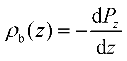
By considering Gauss’ law, the polarization density is related to the bound charge density (ρb):
| −∇·P = ρb. | (2) |
The surface is modeled with a perovskite slab oriented perpendicular to the z-axis with the layer of molecular dipoles deposited at the surface (see ESI, Fig. S3†). The interaction between surface and molecules leads to the additivity of two dipoles: (i) the intrinsic dipole of the ligands or molecules (vide infra) and (ii) the dipole ascribed to the interaction between the molecules and surface. The net interaction eventually leads to a shift in perovskite surface energetics. The slab structure is built in such a way that the dipole density is vanishing in the middle bulk like region of the slab (z = z0 = 0, considered as the origin) while it is also vanishing in the middle of the vacuum region (at  ).
).
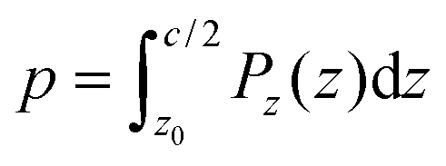
We consider the planar averaged charge density along z (ρb(z)) concomitant with the density profile of the polarization density along the z axis (Pz)
 | (3) |
The weighted integral of the charge density between z0 and  can be computed from a DFT simulation of the slab
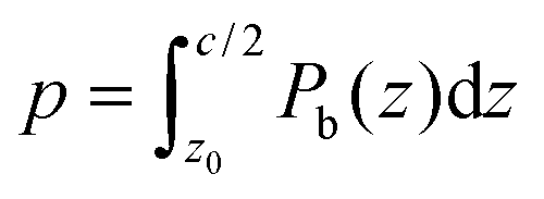 | (4) |
 | (5) |
In order to get some insight into the various contributions close to the surface, a polarization density profile can be extracted by a partial integration of the weighted charge density 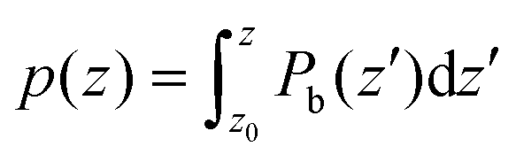 (see Leung et al.20) or Pb(z) can be represented directly as in the work of Traoré et al.22
 | (6) |
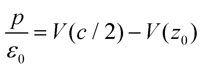
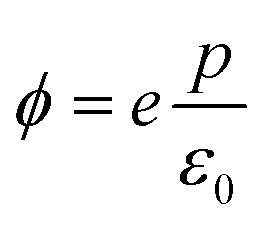
The work function ϕ is given by eV(c/2) − eV(z0) (Fig. S3†), leading to
 | (7) |
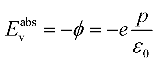
It is possible in the case of DFT calculations performed on semiconductors at T = 0 K (ref. 22) to directly relate the work function to the energy at the top of the valence band (Eabsv, Fig. S3†). Therefore eqn (7) can be written as
 | (8) |
 | (9) |
Investigated ligands
Fig. 1 shows various ligands or molecules that have been considered in this work. The names of the following are 5-carbon chain phosphonic acid (pentylphosphonic acid (C5H13O3P)), 5-carbon chain oleic acid (pentanoic acid), commonly known as valeric acid (C5H10O2), dimethyl sulfoxide (DMSO) ((CH3)2SO), aniline (C6H5NH2) and its derivatives such as p-nitroaniline (aniline –NO2 (C6H6N2O2)), p-methoxyaniline or p-anisidine (C5H9NO) (aniline –OCH3).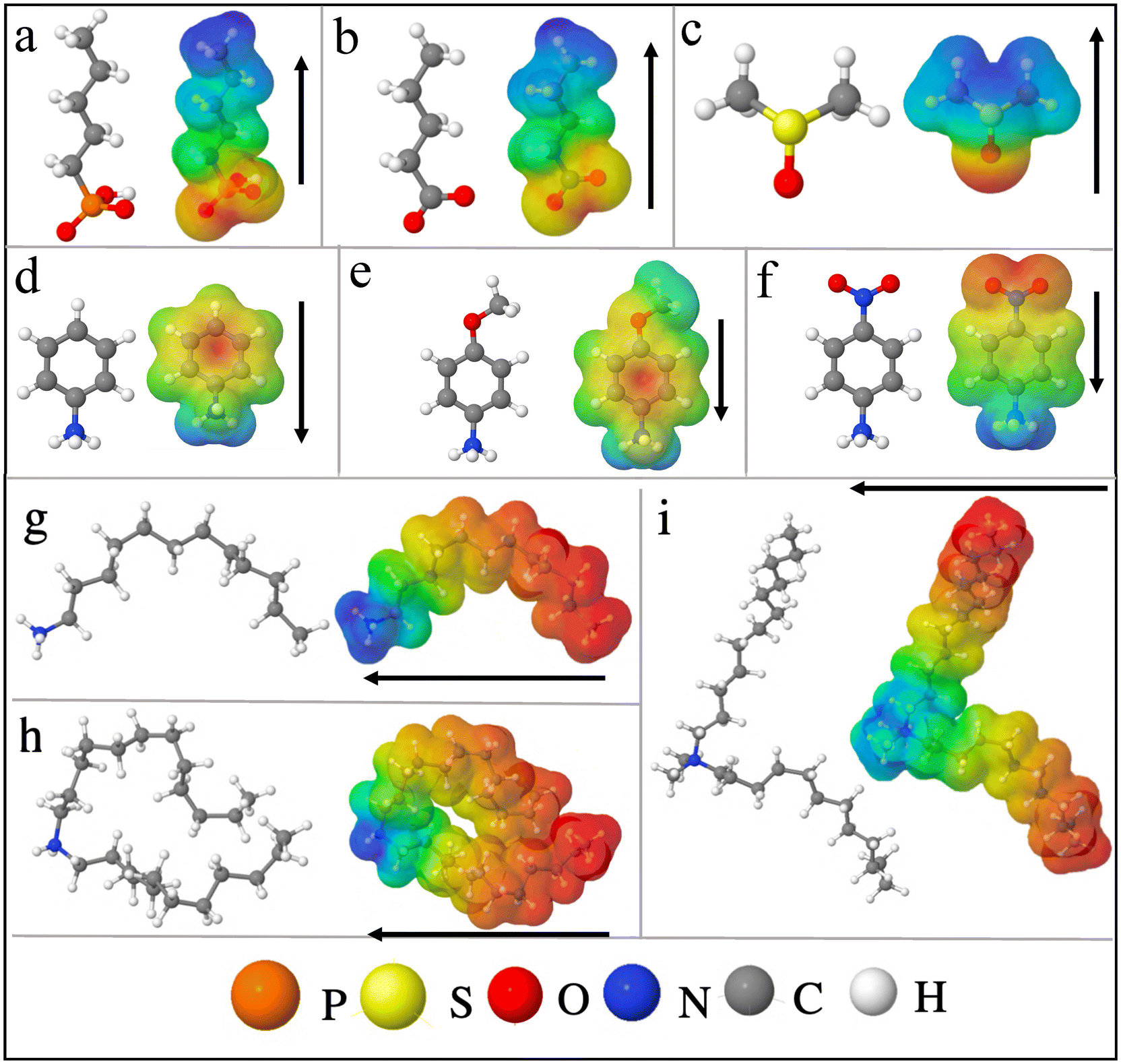 | ||
| Fig. 1 Molecules and their Hirshfeld charge analysis to show the direction of the dipole moment (a) phosphonate (b) oleate (c) DMSO (d) anilinium (e) anilinium –OCH3 (f) anilinium –NO2. Alkylammonium ligands are taken from classical MD simulation snapshots of ref. 42: (g) primary dodecylammonium (DA) (h) secondary didodecylammonium (DDA), and (i) quaternary dimethyldidodecylammonium (DMDDA). The Red (blue) region corresponds to excess electronic charge (electron deficiency). Black arrows show the direction of the dipole moments (see Fig. S3† for sign convention). | ||
Note that for Pentanoic acid and Pentylphosphonic acid, we consider their conjugate base i.e. Pentanoate (C5H9O2−) and Hydrogen phosphonate (C5H12O3P−). For aniline, nitroaniline, and methoxyaniline (see ESI, Fig. S4†), the corresponding conjugate acids are anilinium (C6H5NH3+), methoxyanilinium (C5H10NO+) and nitroanilinium (C6H7N2O2+). For the sake of simplicity, we refer to the considered molecules as phosphonate, oleate, DMSO, anilinium, anilinium –OCH3 and anilinium –NO2.
In addition, we consider three different alkylammonium ligands i.e. primary dodecylammonium (DA), secondary didodecylammonium (DDA), and quaternary dimethyldidodecylammonium (DMDDA). Note that, these ligands are taken from equilibrated snapshots of classical molecular dynamics (MD) simulations, so that dynamic effects are reflected in the alkyl chain of the molecules.42
As a first step, the distribution of charges in the molecules is shown via Hirshfeld charge analysis. The red (blue) region corresponds to a more negative charge (more positive charge) (see Fig. 1). Convention used for the dipole moment direction is from negative to positive charge (Fig. S3(a)†). We calculate the dipole moments of the optimized molecular structures. See Table 1 for a comparison with available experimental or theoretical data from the literature.
Molecules such as phosphonate, oleate, and DMSO act as Lewis bases (electron donating), while anilinium and its derivatives act as Lewis acids with a tendency to withdraw electrons. It is worth noting that there is a relation between the electron-withdrawing/donating nature of molecules and the shift in valence levels. Lewis acid/base interactions with the surface involve charge transfer, i.e. directly associated with the surface dipole density, which can be quantified using eqn (3)–(5). The surface dipole density, in turn, has an impact on the valence energy, as described by eqn (8) and (9).
Among all molecules, aniline –NO2 presents the strongest dipole. The dipole moment of the charged molecules such as DA, DDA and DMDDA, with respect to their center of mass as the origin, are calculated as 25.45 D, 19.84 D and 16.84 D, respectively. These values are consistent with the trend obtained for amines in the literature.47 Notably, values of charged molecules are origin dependent.
Surface–ligand interaction to tune surface dipole density and work function
Firstly, we test the robustness of our methodology by inspecting slabs of CsPbBr3 without functionalization of the surfaces. We construct a CsPbBr3 slab from its pseudo-cubic structure27 so as to avoid issues related to symmetry breaking (see ESI for detailed discussion, Fig. S1c†). We consider the CsBr terminated surface, which appears to be more stable as compared to PbBr2 terminated one.48 We confirm this by comparing the surface energies of the CsBr and PbBr2 terminated surfaces (see ESI, section V†).Thus, we mainly proceed with the CsBr terminated surface of CsPbBr3, considering a slab having 8 octahedra layers (for convergence see ESI, section I†) to study the effect of surface functionalization. To compare various approaches for the work function shifts, charge density, polarization density profiles, surface dipole densities and Hartree potential alignments are computed.
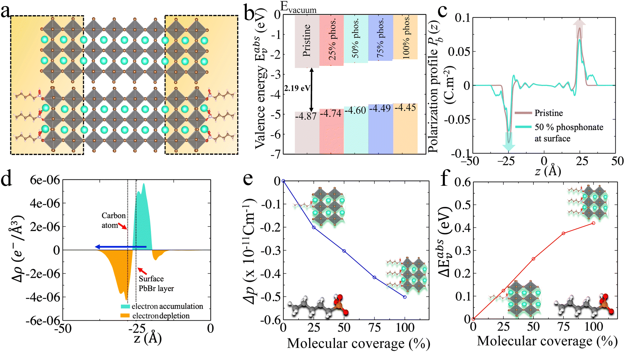 | ||
| Fig. 2 (a) CsPbBr3 CsBr terminated slabs without (top) and with (bottom) phosphonate ligands attached to the surface. The later is illustrated for 50% molecular coverage. (b) Valence energies for 0% to 100% surface coverage. (c) Polarization density profiles for 0% and 50% molecular coverage (for other concentrations see ESI, Fig. S7†). The integration of these polarization profiles result in the surface dipole densities (Table 2). (d) Variation of the electronic charge density upon functionalization with phosphonate for 50% molecular coverage. For clarity, only one side of the symmetric slab is shown. Orange and turquoise color represent electronic depletion and accumulation region, respectively, and the arrow indicates the net dipole direction. (e) Relation between the change in surface dipole density and the molecular coverage. (f) Relation between the change in the valence energies and the molecular coverage. The valence energy values are computed from the Hartree potential profiles. | ||
| E absv (eV) | ΔEabsv [HP] (eV) | p × 10−11 (C m−1) | Δp × 10−11 (C m−1) | ΔEabsv (eV) [eqn (9)] | |
|---|---|---|---|---|---|
| CsPbBr 3 slab with phosphonate concentration | |||||
| Pristine | −4.87 | — | +3.50 | — | — |
| 25% phosphonate | −4.73 | +0.14 | +3.30 | −0.20 | +0.23 |
| 50% phosphonate | −4.60 | +0.27 | +3.20 | −0.30 | +0.34 |
| 75% phosphonate | −4.49 | +0.38 | +3.08 | −0.42 | +0.47 |
| 100% phosphonate | −4.45 | +0.42 | +3.00 | −0.50 | +0.56 |
| CsPbBr 3 slab with oleate concentration | |||||
| Pristine | −4.87 | — | +3.50 | — | — |
| 25% oleate | −4.63 | +0.24 | +3.20 | −0.30 | +0.34 |
| 50% oleate | −4.37 | +0.50 | +2.96 | −0.54 | +0.61 |
| 75% oleate | −4.20 | +0.67 | +2.83 | −0.67 | +0.76 |
| 100% oleate | −4.16 | +0.71 | +2.77 | −0.73 | +0.83 |
| CsPbBr 3 slab with DMSO concentration | |||||
| Pristine | −4.87 | — | +3.50 | — | — |
| 25% DMSO | −4.52 | +0.35 | +3.14 | −0.36 | +0.41 |
| 50% DMSO | −4.14 | +0.73 | +2.80 | −0.70 | +0.79 |
| 75% DMSO | −3.82 | +1.05 | +2.53 | −0.97 | +1.10 |
| 100% DMSO | −3.31 | +1.56 | +2.07 | −1.43 | +1.62 |
To understand the microscopic origin of these shifts, we compute their polarization density profiles (Pb(z)) shown in Fig. 2(c) and analyze the surface and interface dipoles. There are few worthy points that can be highlighted from these polarization profiles (Pb(z)): (i) the surface dipoles counteract each other on both sides of the structure as expected from the symmetry of the slab, (ii) the dipole vanishes in the middle of the slab, (iii) by integrating the area under the peaks of the profiles (Pb(z)) from the center of the slab to the middle of the vacuum (eqn (5)), the surface dipole density (p) can be determined. The computed values of surface dipole densities and the change in surface dipole densities (Δp) for different concentrations (0–100%) are given in Table 2. From Fig. 2, we attribute the increase of Eabsv for phosphonate to the decrease in surface dipole density induced by surface functionalization. The decrease in surface dipole density can be further explained as a result of electron transfer from the phosphonate to the outer perovskite layer, yielding a dipole direction away from the surface (see Fig. 2(d)). We examine this in more depth by looking into the interplay of octahedral tilting in the surface layer and contraction or expansion of PbBr bond lengths at the surface (see ESI, section VII†). We observe from Table S5† that when we compare 25% concentration to other concentrations (50%, 75% and 100%), the surface layers are more distorted with smaller in-plane Pb–Br–Pb angles and much larger out of plane delta (δ (ref. 55)) octahedra tilt angles. It is well known that octahedral tilting significantly influence the electronic properties.56,57 Larger deviations from 180° in Pb–Br–Pb bond angle result in deeper valence levels. This indicates that surface relaxation addtionally impacts the dipole density at the surface, which in turn influence the valence energy. Our conclusion from the aforesaid discussion is that by varying the surface coverage with phosphonate, the work function can be tuned by several meVs with a valence level shifted upwards with increasing coverage.
Next, we extend our discussion to the oleic acid and DMSO molecules, generally used as a surfactant to fabricate colloidal quantum dots.58–60 The details regarding how these molecules are attached on the surface50 are given in ESI (section VIII†). The calculated Eabsv and surface dipole density values for various concentrations are given in Table 2. The increase in Eabsv or upward shift in valence level for oleate anions and DMSO are induced by the reduction of surface dipole density as a result of charge transfer from the molecule to the outer perovskite layer (see ESI, section VIII†). Between 75% and 100% concentration of phosphonate and oleate anions, there is only a minor change in the Eabsv values (∼0.04 eV). It is due to the steric hindrance of bulky molecules (phosphonate and oleate) that impedes the relaxation of the surface (ESI, section VII†), which is not observed with DMSO. For lower surface coverages, the changes in surface dipole density (Δp) and the shift in the valence energies (ΔEabsv) as a function of molecular coverage for phosphonate anions are linear (see Fig. 2(e) and (f)). The linearity relationship also holds for oleate anions and DMSO (ESI, Fig. S12†). Noteworthy, the ΔEabsv obtained from Hartree potential alignment are in agreement with ΔEabsv computed using eqn (9) (see Table 2).
To sum up the aforementioned results, all the studied cases show an upwards shift of the valence level with an increase in the concentration of molecules on the surface. The observed trend is DMSO > oleate > phosphonate in effectively tuning the Eabsv energies. These molecules may also act as potential passivating agents as they do not present any molecular states in between their perovskite-based band edges (ESI, Fig. S13†).
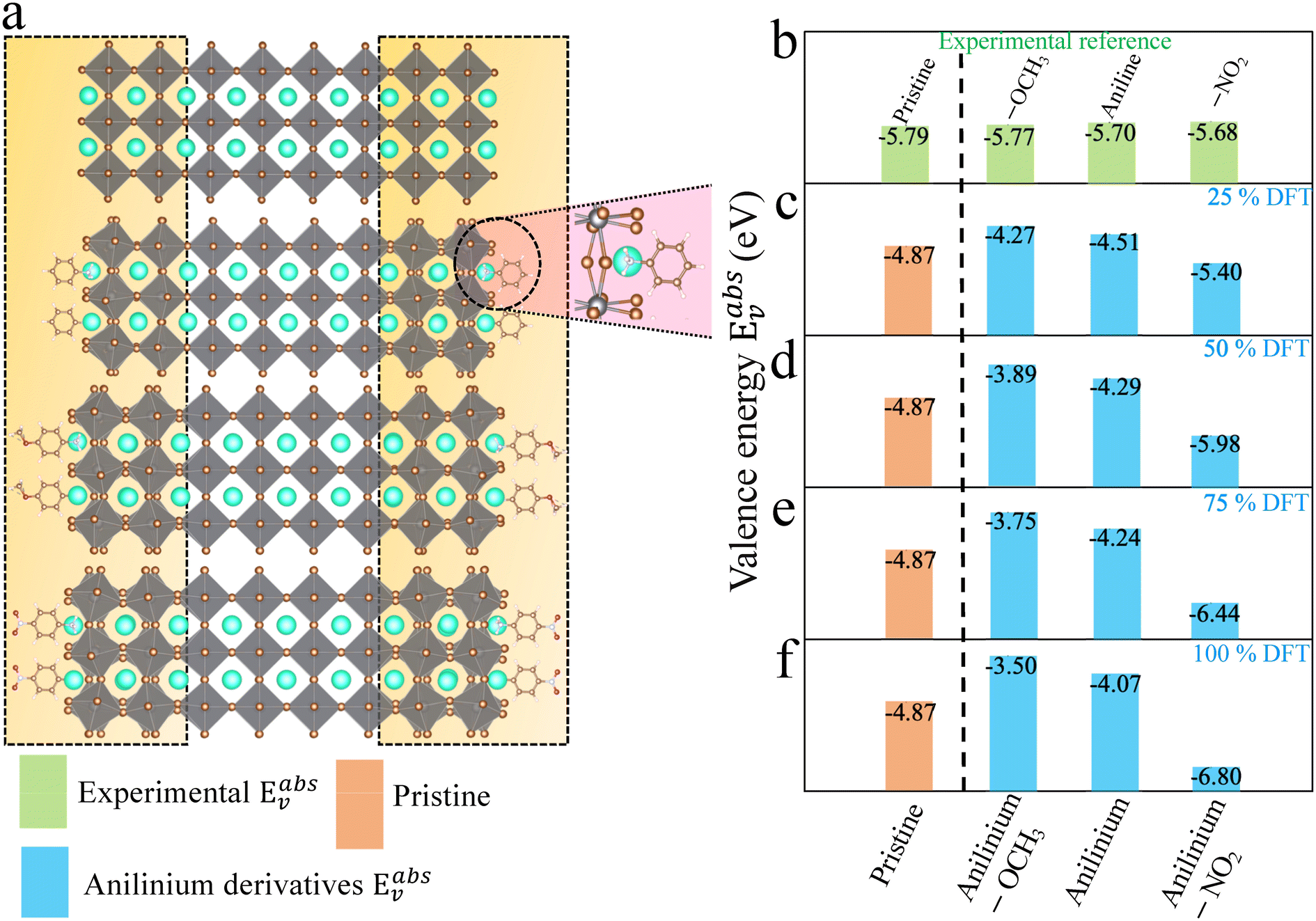 | ||
| Fig. 3 (a) CsPbBr3 CsBr terminated slabs without (top) and with anilinium, anilinium –OCH3 and anilinium –NO2 ligands on the surface. The NH3+ group is placed at a Cs-vacancy of the outer layers on each side of the surface (see zoom view) and is illustrated for 50% molecular coverage. (b) Experimental valence energies (top, green)24 and (c–f) computed Eabsv for pristine (orange) and for (c) 25%, (d) 50%, (e) 75%, and (f) 100% surface coverage (blue). | ||
Comparison between primary, secondary and quaternary alkylammonium ligands
Recently alkylammonium ligands, particularly DMDDA halides, have attracted considerable interest in obtaining purifiable and stable colloids.40,61,62 In light of this, we applied the present methodology to a comparison between three different alkylammonium ligands namely DA, DDA and DMDDA. We have used extracted orientations of long alkyl chain of ligands from classical MD simulations.42 Notably, solid-state NMR spectroscopy confirmed that CsPbBr3 QDs are CsBr terminated with alkylammonium ligands, partially substituting Cs cations at the surface.63 Thus, we substitute Cs+ with the alkylammonium ligand, replacing the cesium by the nitrogen of NH3+, NH2+ and N+ groups corresponding to DA, DDA and DMDDA molecules, respectively (Fig. 4(a)). The computed Eabsv values for DA, DDA and DMDDA are given in Table 3. As previously demonstrated, the observed trend is related to the change in surface dipole density values (Δp) obtained by integrating the area under the peak of (Pb(z)) shown in Fig. 4(c). We obtain small differences between the three alkylammonium ligands, including small structural distorsions of the octahedra at the surface (Table S9†). Still, experimental values may change more significantly, depending on various aspects such as surface doping, molecular coverage, molecular orientations and induced lattice strain at the surface.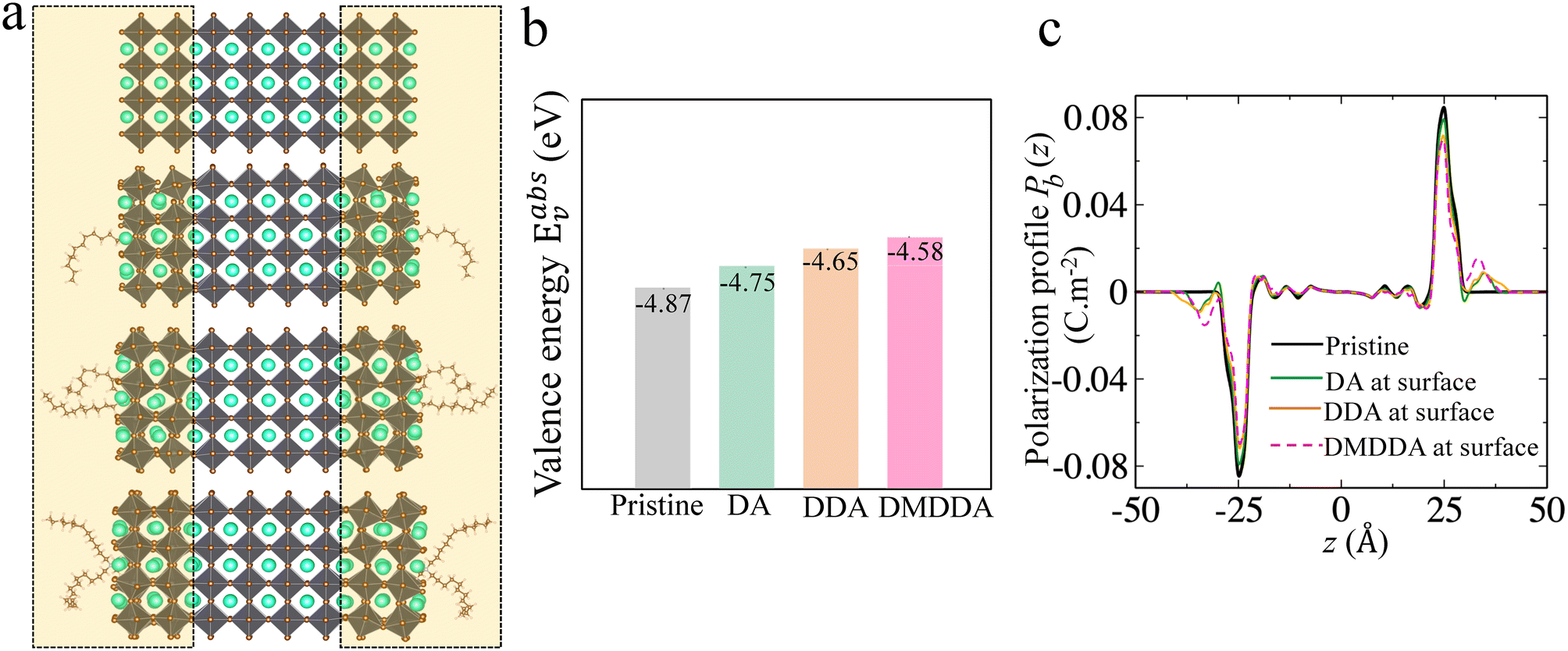 | ||
| Fig. 4 (a) CsPbBr3 CsBr terminated slabs without (top) and with DA, DDA and DMDDA ligands on the surface for a coverage of 11%. Corresponding (b) valence energies and (c) polarization density profiles. | ||
| E absv (eV) | ΔEabsv [HP] (eV) | Δp × 10−11 (C m−1) | ΔEabsv (eV) [eqn (9)] | |
|---|---|---|---|---|
| Pristine | −4.87 | — | — | — |
| DA | −4.75 | +0.12 | −0.18 | +0.20 |
| DDA | −4.65 | +0.22 | −0.25 | +0.28 |
| DMDDA | −4.58 | +0.29 | −0.32 | +0.36 |
Additivity of surface dipole densities and electric susceptibilities
Hitherto, we have investigated different ligands on the CsPbBr3 surface, resulting in positive or negative surface dipole density variations. The increase/decrease in the valence energies is directly linked to the dipole density of the individual components comprising the whole structure.22 Hence, it is interesting to disentangle the individual role of each entity at the interface. We illustrate this decomposition by considering two cases (i) DMSO and (ii) Aniline –NO2 on a CsBr terminated CsPbBr3 surface. Fig. 5(a) and (b) present the polarization density profiles (Pb(z)) of one side of the symmetric slab computed for the pristine perovskite (CsBr slab), the distorted pristine (distortion in the outer layer of the slab due to Cs vacancies), the isolated molecule, and the whole structure. The addition of Pb(z) profiles of the distorted pristine (top panel) and the isolated molecule (middle panel) reproduce the Pb(z) profile of the whole structure (bottom panel). From these Pb(z) profiles, we notice that at the interface, the DMSO molecule counteracts the pristine perovskite (Fig. 5(a)), resulting in a net reduction of the surface dipole density, that subsequently lowers the work function, leading to the upwards shift of the valence level. On the contrary, aniline –NO2 molecule (anilinium –NO2 is shown in ESI, Fig. S20(a)†) allows to significantly increase the surface dipole density (Fig. 5(b)), with an opposite effect on the valence energy and work function.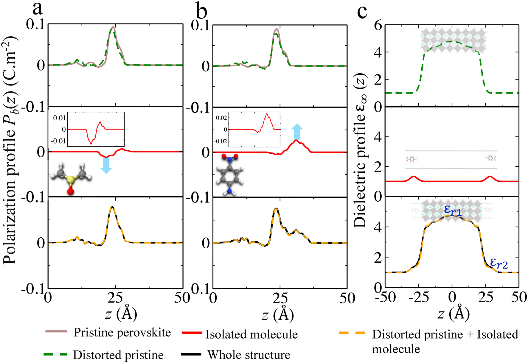 | ||
| Fig. 5 Additivity of surface dipoles densities illustrated with the plot of the polarization density profiles (Pb(z)) computed for (a) DMSO and (b) aniline –NO2 ligands on a CsBr terminated CsPbBr3 surface. A zoom view is shown as inset for isolated molecules. Additivity of electric susceptibilities illustrated with the plot of the position dependent high frequency dielectric profiles (ε∞(z)) computed for (c) aniline –NO2 ligand on a CsBr terminated CsPbBr3 surface. Here, the –NH2 group of aniline –NO2 is pointing towards the surface. | ||
Fig. 5(a) and (b) present the polarization density profiles (Pb(z)) of one side of the symmetric slab computed for the pristine perovskite (CsBr slab), the distorted pristine (distortion in the outer layer of the slab due to Cs vacancies), the isolated molecule, and the whole structure. The addition of Pb(z) profiles of the distorted pristine (top panel) and the isolated molecule (middle panel) reproduce the Pb(z) profile of the whole structure (bottom panel). From these Pb(z) profiles, we notice that at the interface, the DMSO molecule counteracts the pristine perovskite (Fig. 5(a)), resulting in a net reduction of the surface dipole density, that subsequently lowers the work function, leading to the upwards shift of the valence level. On the contrary, aniline –NO2 molecule (anilinium –NO2 is shown in ESI, Fig. S20(a)†) allows to significantly increase the surface dipole density (Fig. 5(b)), with an opposite effect on the valence energy and work function.
We may inspect also the different contributions to the dielectric constant profile. Notably, the interfacial contribution to the dielectric constant profile has already been investigated in the literature using state-of-the-art first-principles approaches.64–66 We use the same method to also show the additivity of the contributions to the electric susceptibility at the surface functionalized by molecular ligands. For that purpose, we compute the position dependent high frequency dielectric profile along the stacking axis (z) for aniline –NO2 and DMSO (see ESI, Fig. S20(b)†) attached on the perovskite surface. Generally, organic molecules have a smaller dielectric constant than the inorganic perovskites. Here, we notice that the bulk dielectric constant i.e. 4.70, in fair agreement with earlier work,49 is nicely captured at the center of the pristine slab. The variation in from εr1 = 4.70 at the center of the dielectric constant profile (pristine distorted) to εr2 = 1.32 (at the position of the isolated molecule) illustrates the presence of dielectric confinement effects (see Fig. 5(c), bottom panel). The dielectric constant profiles of the whole structures (bottom panel) are reasonably well decomposed into their individual counterparts (top and middle panel), using the following equation:67
| εwhole structure∞(z) = εpristine distorted∞(z) + εisolated molecule∞(z) − 1 | (10) |
Revisiting the classical capacitor model for molecular functionalization of halide perovskite surfaces
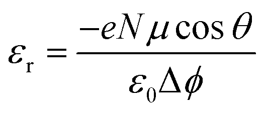
We end up by revisiting the conventional classical approach based on a capacitor model.19,68,69 This approach has been widely used in the context of deposition of molecules on Au metal surfaces70 or TiO2 surfaces.71,72 Within this model, the work function at the surface is modulated by −eΔV, so that Δϕ = −eΔV. The expression for Δϕ is computed from the Poisson's equation, given by: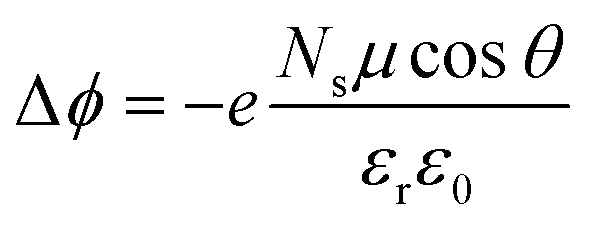 | (11) |
| Molecules | Δϕ = −ΔEabsv | μ (D) | θ (°) |
μ![[thin space (1/6-em)]](https://www.rsc.org/images/entities/char_2009.gif) cosθ (D) cosθ (D) |
|
ε r1 | ε r2 |
|---|---|---|---|---|---|---|---|
| Pentylphosphonic acid (phosphonate) | −0.14 | 1.40 | 8.20 | 1.38 | 2.53 | 4.7 | 1.19 |
| Pentanoic acid (oleate) | −0.24 | 1.59 | 20.69 | 1.49 | 1.59 | 4.7 | 1.15 |
| DMSO | −0.35 | 3.79 | 52 | 2.33 | 1.71 | 4.7 | 1.12 |
| Aniline | +0.40 | 1.70 | 171.96 | −1.68 | 1.08 | 4.7 | 1.22 |
| Aniline –OCH3 | +0.23 | 1.61 | 174.49 | −1.60 | 1.78 | 4.7 | 1.27 |
| Aniline –NO2 | +1.61 | 7.44 | 173.76 | −7.39 | 1.18 | 4.7 | 1.32 |
Conclusions
In summary, we present a methodology that links the change in surface dipole density to the work function using the classical Maxwell's equation and the output from first-principles calculations. Using CsPbBr3 slabs, we illustrate how surface functionalization via tuning the dipole and geometry of ligands effectively controls the work function, with information down to the atomic level. The valence level shifts can be rationalized based on the detailed knowledge of surface dipoles, surface dipole densities, charge transfer as well as local strain effects at the interface as a result of surface–ligand interaction. We observe a continuous decrease in the surface dipole densities correlated with upwards shift of the valence level for DMSO, oleate and phosphonate ligands. A similar behavior is observed for primary, secondary and quaternary alkylammonium ligands, with comparable small changes for all three. Influence of chemical engineering of the surface is further illustrated considering aniline/anilinium and their nitro and methoxy derivatives. Our approach predicts a downward shift of the valence levels that is not experimentally observed, highlighting the limitations of the considered defect and dopant-free surface models. Comparison of results obtained within the present framework with those predicted from the classical capacitor model exemplifies the rather arbitrary choice needed for the effective dielectric constant needed in the later. Overall, our computational strategy provides a useful approach to design and fine tune the energetics of surfaces and interfaces for optimized optoelectronic devices, well beyond the specific case of metal halide perovskites.Computational details
DFT calculations are performed on basis set of finite-range of numerical atomic orbitals implemented in SIESTA code.73,74 We use van der Waals density functional with C09 exchange75 within the van derWaals DF2 flavor to describe the exchange–correlation term for optimizing the atomic positions of the structures. We use a modified version of the SIESTA software “master-post-4.1-251” to include DF2 flavor. This tuning has been suggested to improveC09 based geometry optimization over that with the original DF1 flavor.76 The structures are fully relaxed using the fast inertial relaxation engine (FIRE) algorithm77 until the structure satisfies the following relaxation criteria (i) the two consecutive ionic steps have an energy difference less than 10−4 eV, and (ii) the maximum forces acting on each atom are less than 0.02 eV Å−1. The single point calculations are performed using the generalized gradient approximation78 (GGA with PBE) functional including spin–orbit coupling79 on top of vdwDF2-C09 optimized structures. To correct the band gaps, Slater half occupation technique,80–82 known as DFT-½ i.e. PBE-½ is used (see ESI, section I.3†). We take a polarized double-zeta basis set with an energy shift of 50 meV for bulk CsPbBr3. To describe accurately the properties of the surfaces, we include orbitals with weight in the vacuum region, known as diffuse orbitals:83 diffuse orbitals (5s, 5p, 5d) for Br atom on the top of two atomic layers on both sides of the slab with 30% diffuse orbital size or cutoff radii. A real space mesh grid energy cutoff of 350 Ry is used for our calculations. For the high-frequency dielectric constant profiles calculations, an electric field of 0.025 eV Å−1 is applied along the [001] direction. A detailed discussion for the computational details is given in ESI, section I.† Note that, to reduce the computational burden, we consider a converged five carbons chain length for oleate and phosphonate (see section IV of the ESI for details†).Conflicts of interest
There are no conflicts to declare.Acknowledgements
Authors acknowledge funding from the European Union's Horizon 2020 program, through an Innovation Action under Grant Agreement No. 861985 (PeroCUBE) and through a FET Open research and innovation action under the Grant Agreement No. 899141 (PoLLoC). J. E. acknowledges the financial support from the Institut Universitaire de France. This work was granted access to the HPC resources of TGCC under the allocations 2021-A0110907682 and 2022-A0110907682 made by GENCI. Authors are grateful to Maksym Kovalenko and Andriy Stelmakh for useful discussions and providing the MD snapshots.References
- A. Kojima, K. Teshima, Y. Shirai and T. Miyasaka, Organometal halide perovskites as visible-light sensitizers for photovoltaic cells, J. Am. Chem. Soc., 2009, 131, 6050–6051 CrossRef CAS PubMed.
- R. J. Sutton, G. E. Eperon, L. Miranda, E. S. Parrott, B. A. Kamino, J. B. Patel, M. T. Hörantner, M. B. Johnston, A. A. Haghighirad and D. T. Moore, et al., Bandgap-tunable cesium lead halide perovskites with high thermal stability for efficient solar cells, Adv. Energy Mater., 2016, 6, 1502458 CrossRef.
- G. R. Yettapu, D. Talukdar, S. Sarkar, A. Swarnkar, A. Nag, P. Ghosh and P. Mandal, Terahertz conductivity within colloidal CsPbBr3 perovskite nanocrystals: remarkably high carrier mobilities and large diffusion lengths, Nano Lett., 2016, 16, 4838–4848 CrossRef CAS PubMed.
- J. H. Heo, S. H. Im, J. H. Noh, T. N. Mandal, C.-S. Lim, J. A. Chang, Y. H. Lee, H.-j. Kim, A. Sarkar and M. K. Nazeeruddin, et al., Efficient inorganic–organic hybrid heterojunction solar cells containing perovskite compound and polymeric hole conductors, Nat. Photonics, 2013, 7, 486–491 CrossRef CAS.
- J. Kang and L.-W. Wang, High defect tolerance in lead halide perovskite CsPbBr3, J. Phys. Chem. Lett., 2017, 8, 489–493 CrossRef CAS PubMed.
- W. S. Yang, B.-W. Park, E. H. Jung, N. J. Jeon, Y. C. Kim, D. U. Lee, S. S. Shin, J. Seo, E. K. Kim and J. H. Noh, et al., Iodide management in formamidinium-lead-halide–based perovskite layers for efficient solar cells, Science, 2017, 356, 1376–1379 CrossRef CAS PubMed.
- L. Dou, Y. M. Yang, J. You, Z. Hong, W.-H. Chang, G. Li and Y. Yang, Solution-processed hybrid perovskite photodetectors with high detectivity, Nat. Commun., 2014, 5, 1–6 Search PubMed.
- H. Cho, S.-H. Jeong, M.-H. Park, Y.-H. Kim, C. Wolf, C.-L. Lee, J. H. Heo, A. Sadhanala, N. Myoung and S. Yoo, et al., Overcoming the electroluminescence efficiency limitations of perovskite light-emitting diodes, Science, 2015, 350, 1222–1225 CrossRef CAS PubMed.
- G. Xing, N. Mathews, S. S. Lim, N. Yantara, X. Liu, D. Sabba, M. Grätzel, S. Mhaisalkar and T. C. Sum, Low-temperature solution-processed wavelength-tunable perovskites for lasing, Nat. Mater., 2014, 13, 476–480 CrossRef CAS PubMed.
- P. Schulz, D. Cahen and A. Kahn, Halide perovskites: is it all about the interfaces?, Chem. Rev., 2019, 119, 3349–3417 CrossRef CAS PubMed.
- B. Wang, H. Li, Q. Dai, M. Zhang, Z. Zou, J.-L. Brédas and Z. Lin, Robust Molecular Dipole-Enabled Defect Passivation and Control of Energy-Level Alignment for High-Efficiency Perovskite Solar Cells, Angew. Chem., 2021, 133, 17805–17811 CrossRef.
- H. J. Lee, A. C. Jamison and T. R. Lee, Surface dipoles: a growing body of evidence supports their impact and importance, Acc. Chem. Res., 2015, 48, 3007–3015 CrossRef CAS PubMed.
- L. Canil, T. Cramer, B. Fraboni, D. Ricciarelli, D. Meggiolaro, A. Singh, M. Liu, M. Rusu, C. M. Wolff and N. Phung, et al., Tuning halide perovskite energy levels, Energy Environ. Sci., 2021, 14, 1429–1438 RSC.
- K.-G. Lim, S. Ahn and T.-W. Lee, Energy level alignment of dipolar interface layer in organic and hybrid perovskite solar cells, J. Mater. Chem. C, 2018, 6, 2915–2924 RSC.
- W. Kong, W. Li, C. Liu, H. Liu, J. Miao, W. Wang, S. Chen, M. Hu, D. Li and A. Amini, et al., Organic monomolecular layers enable energy-level matching for efficient hole transporting layer free inverted perovskite solar cells, ACS Nano, 2019, 13, 1625–1634 CrossRef CAS PubMed.
- K. Hills-Kimball, H. Yang, T. Cai, J. Wang and O. Chen, Recent Advances in Ligand Design and Engineering in Lead Halide Perovskite Nanocrystals, Adv. Sci., 2021, 2100214 CrossRef CAS PubMed.
- W. Melitz, J. Shen, A. C. Kummel and S. Lee, Kelvin probe force microscopy and its application, Surf. Sci. Rep., 2011, 66, 1–27 CrossRef CAS.
- I. D. Baikie, A. C. Grain, J. Sutherland and J. Law, Ambient pressure photoemission spectroscopy of metal surfaces, Appl. Surf. Sci., 2014, 323, 45–53 CrossRef CAS.
- R. J. Demchak and T. Fort Jr., Surface, Dipole moments of close-packed un-ionized monolayers at the air-water interface, J. Colloid Interface Sci., 1974, 46, 191–202 CrossRef CAS.
- T. Leung, C. Kao, W. Su, Y. Feng and C. Chan, Relationship between surface dipole, work function and charge transfer: Some exceptions to an established rule, Phys. Rev. B: Condens. Matter Mater. Phys., 2003, 68, 195408 CrossRef.
- Y. Zheng, Z. Fang, M. Shang, Q. Sun, J. Zheng, Z. Yang, X. Hou and W. Yang, Linearly Tailored Work Function of Orthorhombic CsSnI3 Perovskites, ACS Energy Lett., 2021, 6, 2328–2335 CrossRef CAS.
- B. Traoré, P. Basera, A. J. Ramadan, H. J. Snaith, C. Katan and J. Even, A Theoretical Framework for Microscopic Surface and Interface Dipoles, Work Functions, and Valence Band Alignments in 2D and 3D Halide Perovskite Heterostructures, ACS Energy Lett., 2021, 7, 349–357 CrossRef.
- J. Zheng, J. Chen, D. Ouyang, Z. Huang, X. He, J. Kim and W. C. Choy, Critical Role of Functional Groups in Defect Passivation and Energy Band Modulation in Efficient and Stable Inverted Perovskite Solar Cells Exceeding 21% Efficiency, ACS Appl. Mater. Interfaces, 2020, 12, 57165–57173 CrossRef CAS PubMed.
- J. Duan, M. Wang, Y. Wang, J. Zhang, Q. Guo, Q. Zhang, Y. Duan and Q. Tang, Effect of Side-Group-Regulated Dipolar Passivating Molecules on CsPbBr3 Perovskite Solar Cells, ACS Energy Lett., 2021, 6, 2336–2342 CrossRef CAS.
- J. Pan, H. Huang, W. Zhao, D. Lin, Z. Nie, J. Zhong, L. Ma and X. Zhang, Efficient and Stable Self-Assembly Blue-Emitting CsPbBr3 Nanoplatelets with Self-Repaired Surface Defects, ACS Appl. Nano Mater., 2022, 5, 15062–15069 CrossRef CAS.
- G. Rainò, G. Nedelcu, L. Protesescu, M. I. Bodnarchuk, M. V. Kovalenko, R. F. Mahrt and T. Stöferle, Single cesium lead halide perovskite nanocrystals at low temperature: fast single-photon emission, reduced blinking, and exciton fine structure, ACS Nano, 2016, 10, 2485–2490 CrossRef PubMed.
- C. C. Stoumpos, C. D. Malliakas, J. A. Peters, Z. Liu, M. Sebastian, J. Im, T. C. Chasapis, A. C. Wibowo, D. Y. Chung and A. J. Freeman, et al., Crystal growth of the perovskite semiconductor CsPbBr3: a new material for high-energy radiation detection, Cryst. Growth Des., 2013, 13, 2722–2727 CrossRef CAS.
- J. Peng, C. Q. Xia, Y. Xu, R. Li, L. Cui, J. K. Clegg, L. M. Herz, M. B. Johnston and Q. Lin, Crystallization of CsPbBr3 single crystals in water for X-ray detection, Nat. Commun., 2021, 12, 1–10 CrossRef PubMed.
- D. N. Dirin, I. Cherniukh, S. Yakunin, Y. Shynkarenko and M. V. Kovalenko, Solution-grown CsPbBr3 perovskite single crystals for photon detection, Chem. Mater., 2016, 28, 8470–8474 CrossRef CAS PubMed.
- Y. Rakita, N. Kedem, S. Gupta, A. Sadhanala, V. Kalchenko, M. L. Böhm, M. Kulbak, R. H. Friend, D. Cahen and G. Hodes, Low-temperature solution-grown CsPbBr3 single crystals and their characterization, Cryst. Growth Des., 2016, 16, 5717–5725 CrossRef CAS.
- R. Chen, Z. Liang, W. Feng, X. Hu and A. Hao, Solution-processed all-inorganic perovskite CsPbBr3 thin films for optoelectronic application, J. Alloys Compd., 2021, 864, 158125 CrossRef CAS.
- Q. A. Akkerman, S. G. Motti, A. R. Srimath Kandada, E. Mosconi, V. DâInnocenzo, G. Bertoni, S. Marras, B. A. Kamino, L. Miranda and F. De Angelis, et al., Solution synthesis approach to colloidal cesium lead halide perovskite nanoplatelets with monolayer-level thickness control, J. Am. Chem. Soc., 2016, 138, 1010–1016 CrossRef CAS PubMed.
- G. Rainò, N. Yazdani, S. C. Boehme, M. Kober-Czerny, C. Zhu, F. Krieg, M. D. Rossell, R. Erni, V. Wood and I. Infante, et al., Ultra-narrow room-temperature emission from single CsPbBr3 perovskite quantum dots, Nat. Commun., 2022, 13, 1–8 Search PubMed.
- I. Cherniukh, G. Rainò, T. Stöferle, M. Burian, A. Travesset, D. Naumenko, H. Amenitsch, R. Erni, R. F. Mahrt and M. I. Bodnarchuk, et al., Perovskite-type superlattices from lead halide perovskite nanocubes, Nature, 2021, 593, 535–542 CrossRef CAS PubMed.
- G. Rainò, M. A. Becker, M. I. Bodnarchuk, R. F. Mahrt, M. V. Kovalenko and T. Stöferle, Superfluorescence from lead halide perovskite quantum dot superlattices, Nature, 2018, 563, 671–675 CrossRef PubMed.
- A. A. Petrov, S. A. Fateev, V. N. Khrustalev, Y. Li, P. V. Dorovatovskii, Y. V. Zubavichus, E. A. Goodilin and A. B. Tarasov, Formamidinium haloplumbate intermediates: the missing link in a chain of hybrid perovskites crystallization, Chem. Mater., 2020, 32, 7739–7745 CrossRef CAS.
- G. Nedelcu, L. Protesescu, S. Yakunin, M. I. Bodnarchuk, M. J. Grotevent and M. V. Kovalenko, Fast anion-exchange in highly luminescent nanocrystals of cesium lead halide perovskites (CsPbX3, X = Cl, Br, I), Nano Lett., 2015, 15, 5635–5640 CrossRef CAS PubMed.
- J. De Roo, M. Ibáñez, P. Geiregat, G. Nedelcu, W. Walravens, J. Maes, J. C. Martins, I. Van Driessche, M. V. Kovalenko and Z. Hens, Highly dynamic ligand binding and light absorption coefficient of cesium lead bromide perovskite nanocrystals, ACS Nano, 2016, 10, 2071–2081 CrossRef CAS PubMed.
- W.-k. Koh, S. Park and Y. Ham, Phosphonic acid stabilized colloidal CsPbX3 (X = Br, I) perovskite nanocrystals and their surface chemistry, ChemistrySelect, 2016, 1, 3479–3482 CrossRef CAS.
- M. Imran, P. Ijaz, L. Goldoni, D. Maggioni, U. Petralanda, M. Prato, G. Almeida, I. Infante and L. Manna, Simultaneous cationic and anionic ligand exchange for colloidally stable CsPbBr3 nanocrystals, ACS Energy Lett., 2019, 4, 819–824 CrossRef CAS.
- A. Franciosi and C. G. Van de Walle, Heterojunction band offset engineering, Surf. Sci. Rep., 1996, 25, 1–140 CrossRef CAS.
- A. Stelmakh, M. Aebli, A. Baumketner and M. V. Kovalenko, On the mechanism of alkylammonium ligands binding to the surface of CsPbBr3 nanocrystals, Chem. Mater., 2021, 33, 5962–5973 CrossRef CAS PubMed.
- C. Schmitt, Surface modification of oxide nanoparticles using phosphonic acids: characterization, surface dynamics, and dispersion in sols and nanocomposites, Ph.D. thesis, Université Montpellier, 2015.
- E. Mognaschi, L. Zullino and A. Chierico, Associating behaviour of pure polar liquids: dielectric properties of n-valeric acid, J. Phys. D: Appl. Phys., 1984, 17, 1007 CrossRef CAS.
- D. R. Lide, CRC handbook of chemistry and physics, CRC press, 2004, vol. 85 Search PubMed.
- S. Itoh and H. Ohtaki, A study of the liquid structure of dimethyl sulfoxide by the X-ray diffraction, Z. Naturforsch., A: Phys. Sci., 1987, 42, 858–862 CrossRef CAS.
- H. Yoneda, Effect of substitution on dipole moments of molecules, Bull. Chem. Soc. Jpn., 1958, 31, 708–714 CrossRef CAS.
- M. I. Bodnarchuk, S. C. Boehme, S. ten Brinck, C. Bernasconi, Y. Shynkarenko, F. Krieg, R. Widmer, B. Aeschlimann, D. Günther and M. V. Kovalenko, et al., Rationalizing and controlling the surface structure and electronic passivation of cesium lead halide nanocrystals, ACS Energy Lett., 2018, 4, 63–74 CrossRef PubMed.
- L. Protesescu, S. Yakunin, M. I. Bodnarchuk, F. Krieg, R. Caputo, C. H. Hendon, R. X. Yang, A. Walsh and M. V. Kovalenko, Nanocrystals of cesium lead halide perovskites (CsPbX3, X = Cl, Br, and I): novel optoelectronic materials showing bright emission with wide color gamut, Nano Lett., 2015, 15, 3692–3696 CrossRef CAS PubMed.
- D. P. Nenon, K. Pressler, J. Kang, B. A. Koscher, J. H. Olshansky, W. T. Osowiecki, M. A. Koc, L.-W. Wang and A. P. Alivisatos, Design principles for trap-free CsPbX3 nanocrystals: enumerating and eliminating surface halide vacancies with softer Lewis bases, J. Am. Chem. Soc., 2018, 140, 17760–17772 CrossRef CAS PubMed.
- B. Zhang, L. Goldoni, J. Zito, Z. Dang, G. Almeida, F. Zaccaria, J. De Wit, I. Infante, L. De Trizio and L. Manna, Alkyl phosphonic acids deliver CsPbBr3 nanocrystals with high photoluminescence quantum yield and truncated octahedron shape, Chem. Mater., 2019, 31, 9140–9147 CrossRef CAS.
- G. Almeida, O. J. Ashton, L. Goldoni, D. Maggioni, U. Petralanda, N. Mishra, Q. A. Akkerman, I. Infante, H. J. Snaith and L. Manna, The phosphine oxide route toward lead halide perovskite nanocrystals, J. Am. Chem. Soc., 2018, 140, 14878–14886 CrossRef PubMed.
- J. Y. Woo, S. Lee, S. Lee, W. D. Kim, K. Lee, K. Kim, H. J. An, D. C. Lee and S. Jeong, Air-stable PbSe nanocrystals passivated by phosphonic acids, J. Am. Chem. Soc., 2016, 138, 876–883 CrossRef CAS PubMed.
- J. Shamsi, D. Kubicki, M. Anaya, Y. Liu, K. Ji, K. Frohna, C. P. Grey, R. H. Friend and S. D. Stranks, Stable hexylphosphonate-capped blue-emitting quantum-confined CsPbBr3 nanoplatelets, ACS Energy Lett., 2020, 5, 1900–1907 CrossRef CAS PubMed.
- L. Pedesseau, D. Sapori, B. Traore, R. Robles, H.-H. Fang, M. A. Loi, H. Tsai, W. Nie, J.-C. Blancon and A. Neukirch, et al., Advances and promises of layered halide hybrid perovskite semiconductors, ACS Nano, 2016, 10, 9776–9786 CrossRef CAS PubMed.
- J. L. Knutson, J. D. Martin and D. B. Mitzi, Tuning the band gap in hybrid tin iodide perovskite semiconductors using structural templating, Inorg. Chem., 2005, 44, 4699–4705 CrossRef CAS PubMed.
- J. Even, L. Pedesseau, J.-M. Jancu and C. Katan, Importance of spin–orbit coupling in hybrid organic/inorganic perovskites for photovoltaic applications, J. Phys. Chem. Lett., 2013, 4, 2999–3005 CrossRef CAS.
- L. Hu, C. Wang, R. M. Kennedy, L. D. Marks and K. R. Poeppelmeier, The role of oleic acid: From synthesis to assembly of perovskite nanocuboid two-dimensional arrays, Inorg. Chem., 2015, 54, 740–745 CrossRef CAS PubMed.
- N. Ahn, D.-Y. Son, I.-H. Jang, S. M. Kang, M. Choi and N.-G. Park, Highly reproducible perovskite solar cells with average efficiency of 18.3% and best efficiency of 19.7% fabricated via Lewis base adduct of lead(II) iodide, J. Am. Chem. Soc., 2015, 137, 8696–8699 CrossRef CAS PubMed.
- R. Vidal, J.-A. Alberola-Borràs, S. N. Habisreutinger, J.-L. Gimeno-Molina, D. T. Moore, T. H. Schloemer, I. Mora-Seró, J. J. Berry and J. M. Luther, Assessing health and environmental impacts of solvents for producing perovskite solar cells, Nat. Sustain., 2021, 4, 277–285 CrossRef.
- Y. Shynkarenko, M. I. Bodnarchuk, C. Bernasconi, Y. Berezovska, V. Verteletskyi, S. T. Ochsenbein and M. V. Kovalenko, Direct synthesis of quaternary alkylammonium-capped perovskite nanocrystals for efficient blue and green light-emitting diodes, ACS Energy Lett., 2019, 4, 2703–2711 CrossRef CAS PubMed.
- J. Pan, L. N. Quan, Y. Zhao, W. Peng, B. Murali, S. P. Sarmah, M. Yuan, L. Sinatra, N. M. Alyami and J. Liu, et al., Highly efficient perovskite-quantum-dot light-emitting diodes by surface engineering, Adv. Mater., 2016, 28, 8718–8725 CrossRef CAS PubMed.
- Y. Chen, S. R. Smock, A. H. Flintgruber, F. A. Perras, R. L. Brutchey and A. J. Rossini, Surface termination of CsPbBr3 perovskite quantum dots determined by solid-state NMR spectroscopy, J. Am. Chem. Soc., 2020, 142, 6117–6127 CrossRef CAS PubMed.
- F. Giustino and A. Pasquarello, Theory of atomic-scale dielectric permittivity at insulator interfaces, Phys. Rev. B: Condens. Matter Mater. Phys., 2005, 71, 144104 CrossRef.
- N. Shi and R. Ramprasad, Atomic-scale dielectric permittivity profiles in slabs and multilayers, Phys. Rev. B: Condens. Matter Mater. Phys., 2006, 74, 045318 CrossRef.
- D. Sapori, M. Kepenekian, L. Pedesseau, C. Katan and J. Even, Quantum confinement and dielectric profiles of colloidal nanoplatelets of halide inorganic and hybrid organic–inorganic perovskites, Nanoscale, 2016, 8, 6369–6378 RSC.
- B. Traore, L. Pedesseau, L. Assam, X. Che, J.-C. Blancon, H. Tsai, W. Nie, C. C. Stoumpos, M. G. Kanatzidis and S. Tretiak, et al., Composite nature of layered hybrid perovskites: assessment on quantum and dielectric confinements and band alignment, ACS Nano, 2018, 12, 3321–3332 CrossRef CAS PubMed.
- O. N. Oliveira, D. M. Taylor, T. J. Lewis, S. Salvagno and C. J. Stirling, Estimation of group dipole moments from surface potential measurements on Langmuir monolayers, J. Chem. Soc., Faraday Trans. 1, 1989, 85, 1009–1018 RSC.
- J. Davies and S. E. Rideal, Interfacial potentials, Can. J. Chem., 1955, 33, 947–960 CrossRef CAS.
- P. C. Rusu and G. Brocks, Surface dipoles and work functions of alkylthiolates and fluorinated alkylthiolates on Au (111), J. Phys. Chem. B, 2006, 110, 22628–22634 CrossRef CAS PubMed.
- C. Goh, S. R. Scully and M. D. McGehee, Effects of molecular interface modification in hybrid organic-inorganic photovoltaic cells, J. Appl. Phys., 2007, 101, 114503 CrossRef.
- T. Zhu, J. Su, J. Alvarez, G. Lefèvre, F. Labat, I. Ciofini and T. Pauporté, Response Enhancement of Self-Powered Visible-Blind UV Photodetectors by Nanostructured Heterointerface Engineering, Adv. Funct. Mater., 2019, 29, 1903981 CrossRef.
- E. Artacho, E. Anglada, O. Diéguez, J. D. Gale, A. García, J. Junquera, R. M. Martin, P. Ordejón, J. M. Pruneda and D. Sánchez-Portal, et al., The SIESTA method; developments and applicability, J. Phys.: Condens. Matter, 2008, 20, 064208 CrossRef PubMed.
- J. M. Soler, E. Artacho, J. D. Gale, A. García, J. Junquera, P. Ordejón and D. Sánchez-Portal, The SIESTA method for ab initio order-N materials simulation, J. Phys.: Condens. Matter, 2002, 14, 2745 CrossRef CAS.
- V. R. Cooper, van der Waals density functional: An appropriate exchange functional, Phys. Rev. B: Condens. Matter Mater. Phys., 2010, 81, 161104 CrossRef.
- I. Hamada and M. Otani, Comparative van der Waals density-functional study of graphene on metal surfaces, Phys. Rev. B: Condens. Matter Mater. Phys., 2010, 82, 153412 CrossRef.
- E. Bitzek, P. Koskinen, F. Gähler, M. Moseler and P. Gumbsch, Structural relaxation made simple, Phys. Rev. Lett., 2006, 97, 170201 CrossRef PubMed.
- J. P. Perdew, K. Burke and M. Ernzerhof, Generalized gradient approximation made simple, Phys. Rev. Lett., 1996, 77, 3865 CrossRef CAS PubMed.
- L. Fernández-Seivane, M. A. Oliveira, S. Sanvito and J. Ferrer, On-site approximation for spin–orbit coupling in linear combination of atomic orbitals density functional methods, J. Phys.: Condens. Matter, 2006, 18, 7999 CrossRef.
- L. G. Ferreira, M. Marques and L. K. Teles, Approximation to density functional theory for the calculation of band gaps of semiconductors, Phys. Rev. B: Condens. Matter Mater. Phys., 2008, 78, 125116 CrossRef.
- S. X. Tao, X. Cao and P. A. Bobbert, Accurate and efficient band gap predictions of metal halide perovskites using the DFT-1/2 method: GW accuracy with DFT expense, Sci. Rep., 2017, 7, 1–9 CrossRef PubMed.
- B. Traoré, J. Even, L. Pedesseau, M. Kepenekian and C. Katan, Band gap, effective masses, and energy level alignment of 2D and 3D halide perovskites and heterostructures using DFT-1/2, Phys. Rev. Mater., 2022, 6, 014604 CrossRef.
- S. García-Gil, A. García, N. Lorente and P. Ordejón, Optimal strictly localized basis sets for noble metal surfaces, Phys. Rev. B: Condens. Matter Mater. Phys., 2009, 79, 075441 CrossRef.
Footnote |
| † Electronic supplementary information (ESI) available: Computational details; definition and convention; investigated ligands; convergence of carbon chain length for the molecules on a CsPbBr3 surface; surface energies of CsBr and PbBr2 terminated slabs; polarization density profile for phosphonate anion on a CsPbBr3 surface; surface relaxation effect on valence levels; detailed results for oleate anion and DMSO molecule on a CsPbBr3 surface; band structure of CsPbBr3 slabs with phosphonate, oleate, DMSO, aniline, aniline –OCH3 and aniline –NO2 (two orientations) as well as anilinium and its derivatives; experimental valence energy positions of aniline, aniline –OCH3 and aniline –NO2-treated CsPbBr3 reported in the literature for perovskite films; additional results on the additivity of surface dipole densities and electric susceptibilities; computed position dependent high frequency dielectric profiles and dielectric constants at the position of the molecules. See DOI: https://doi.org/10.1039/d3nr01126g |
| This journal is © The Royal Society of Chemistry 2023 |