DOI:
10.1039/D3NR00988B
(Paper)
Nanoscale, 2023,
15, 9372-9389
Tunable near-infrared emission and three-photon absorption in lanthanide-doped double perovskite nanocrystals†
Received
2nd March 2023
, Accepted 20th April 2023
First published on 20th April 2023
Abstract
Cs2AgInCl6 double perovskite (DP) nanocrystals (NCs) are an emerging class of materials with promising application potential in photonics/optoelectronics owing to their nontoxicity, direct bandgap, and high thermal and moisture stability. These NCs are, however, rarely explored for nonlinear optical (NLO) applications. Herein, we present a comprehensive investigation of the photophysical and nonlinear optical properties of erbium- (Er) and ytterbium (Yb)-doped Cs2AgInCl6 nanocrystals (denoted as Er-DP and Yb-DP, respectively). Temperature-dependent photoluminescence of these NCs was analyzed to estimate their exciton binding energy, Huang–Rhys parameter (S), and electron–phonon coupling strength, which are of fundamental interest to gain an in-depth understanding of the material systems. Femtosecond Z-scan experiments with 800 nm excitation revealed the reverse saturable absorption (RSA) behavior owing to three-photon absorption (3PA). The obtained values of the 3PA coefficients were 1.35 × 10⁻⁴ and 1.64 × 10⁻⁴ cm3 GW−2, respectively, and the nonlinear refractive indices were estimated to be 1.02 × 10⁻¹⁵ and 1.15 × 10⁻¹⁵ cm2 W−1, respectively, for Er-DP and Yb-DP. These values are superior to those obtained in undoped Cs2AgInCl6 NCs. The physical parameter, Kane energy, which is closely related to the magnitude of the oscillator strength, was estimated to be 25 eV and 26 eV for Er-DP and Yb-DP, respectively. As a proof-of-concept application, we further obtained the optical limiting onset and figure of merit to reveal their prospect as an optical limiter and in photonic switching application. With such emission and nonlinear optical properties, we anticipate that lanthanide-doped Cs2AgInCl6 NCs can be used for designing eco-friendly nonlinear optoelectronic/photonic devices.
Introduction
Lead-free halide double perovskites, such as Cs2AgInCl6, Cs2AgBiX6, Cs2NaInCl6, Cs2AgSbX6, and Cs2NaBiCl6, have been identified as a potential alternative to conventional lead (Pb)-based halide perovskites for optoelectronic applications over the last few years.1–6 Despite the excellent properties exhibited by Pb–halide perovskites,7 low stability and the presence of lead increase their apparent toxicity and restrict their commercialization into consumer electronics.8 The development of new classes of semiconductor materials that can address toxicity and stability concerns while retaining the intriguing capabilities of Pb-based perovskite materials has therefore gained tremendous interest. Replacing lead with harmless elements is one of the most promising ways to develop such materials. Sn2+, Ge2+, Bi3+, and Sb3+ cations have been investigated as Pb2+ replacements in perovskites during the last few years. However, Sn- and Ge-based halide perovskites are less stable and quickly degrade in the presence of oxygen and moisture,9 whereas Bi- and Sb-based halide perovskite structures have less symmetry than the typical perovskite structure, which causes less dimensional connection of the octahedral structure and less electronic mobility,10 eventually impairing the performance of final devices.
Halide double perovskites (HDPs) with the general formula A2M(I)M(III)X6 (A is a monovalent organic or inorganic cation, M(I) is a monovalent metal cation, M(III) is a trivalent metal cation, and X is a halide anion) have shown the most promise among the several attempts to substitute Pb.11 Among the several HDP systems explored, one of the promising material systems is Cs2AgInCl6, exhibiting a direct bandgap,12 broad emission spectra, and high structural stability against moisture and heat. The broad emission spectra originate from self-trapped excitons (STEs) related to the Jahn–Teller distortion of [AgCl6]5− octahedra.13,14 The structural robustness and direct bandgap characteristics make Cs2AgInCl6 NCs an ideal lead-free alternative in the field of optoelectronics. There are several reports1,4,14,15 on doping and co-doping into Cs2AgInCl6 to improve its optoelectronic properties. Doping with rare-earth elements has been shown to be an effective way of tuning the phosphors’ emission spectra.16 Trivalent lanthanides (Ln3+) favor octahedral or higher coordination locations.17 This becomes a significant factor in why Ln3+ doping in APbX3 perovskites has recently continued to be effective.18 With two states 2F5/2 and 2F7/2, Yb3+ has one of the simplest valence f–f energy level configurations, resulting in intense NIR emission17 at 990 nm, which can be effectively used for NIR light-emitting diodes and sensors. The NIR emission at 1540 nm of Er3+ is ideal for optical telecommunications with low loss. Locardi et al. showed an efficient colloidal method for synthesizing Cs2AgInCl6 NCs and Mn-doped Cs2AgInCl6 NCs with good control over the end product's size distribution.1 The synthesis of Er- and Yb-doped Cs2AgInCl6 colloidal NCs was reported by Lee et al.; they have studied the absorption and photoluminescence properties of doped Cs2AgInCl6 NCs and the effect on the crystallinity of NCs after doping.19 Although a few research studies have been conducted on DPNCs and their doped counterparts, rigorous investigation on Cs2AgInCl6 NCs is still required with respect to their optical properties such as the photoluminescence (PL) mechanism-driven parameters of PL. Furthermore, STE properties of pristine Cs2AgInCl6 NCs are not clear to date. This ambiguity will limit the use of DPNCs in the field of optoelectronics.
Nonlinear optical effects have become a cornerstone for the manipulation of photons in cutting-edge technologies, including optical computation, information processing and storage, and telecommunications, due to the formation of new secondary optical fields and the alteration of the phase and frequency induced by polarization.20–22 To understand the complex optical phenomena seen in halide perovskite materials, a more profound comprehension of their nonlinear optical coefficients is necessary. Furthermore, the precise determination of optical coefficients can be considered as the study of the fundamental photophysics of semiconductors. The nanocrystal geometries of semiconductors have a promising influence on the NLO characteristics.23 The high confinement of the perovskite materials will enhance both their linear optical and NLO properties. These features are advantageous for high performance in NLO and photonic applications. The shape of NCs modifies the physicochemical and optoelectronic characteristics of colloidal NCs for efficient use in a variety of applications.24 Recently, nonlinear optical phenomena of perovskites,25,26 such as optical modulation,27 lasing,28 and high-harmonic generation,29 have been explored with much interest. Several studies on perovskite nanocrystals have demonstrated their development as outstanding optical materials in NLO and electrical responses owing to the multiphoton absorption. The strong two-photon absorption (2PA) of Cs2AgIn0.9Bi0.1Cl6 nanocrystals was explored under the excitation of an 800 nm, 57 fs laser.30 The NLO characteristics of Cs2AgBiBr6 double perovskite NCs were examined with a 2PA cross-section of ∼1906 GM and a 2PA coefficient of ∼10−11 cm W−1 by Zhang et al.31 Furthermore, they have also determined the nonlinear absorption coefficient of Cs4CuxAg2−2xSb2Cl12 nanocrystals to be ∼10−8 cm W−1 using an 800 nm, 500 Hz fs laser.32 Khanam et al.33 studied the three-photon absorption (3PA) coefficient of SrCl2-doped FAPbBr3 NCs and obtained a 3PA cross-section of ∼10−77 cm6 s2. Our group has carried out broadband ultrafast nonlinear optical studies of zero-dimensional Cs4PbBr6 perovskite films34 and CsPbBr3 NCs,35 unveiling their photonic responses in the NLO domain. If we talk about rare-earth-doped materials,36 they show good NLO activities. However, no reports are found on the NLO properties of lanthanide-doped halide perovskites. In this work, we have prepared Cs2AgInCl6 NCs, Er-doped Cs2AgInCl6 NCs, and Yb-doped Cs2AgInCl6 NCs abbreviated as DP, Er-DP, and Yb-DP, respectively, and have presented a comprehensive picture of their photophysical properties in detail and then have explored their ultrafast NLO characteristics for photonic applications. The structural details of these DPNCs have been explored using X-ray diffraction (XRD), transmission electron microscopy (TEM), and selected area electron diffraction (SAED) patterns. Optical absorption, PL, photoluminescence excitation (PLE), and PL decay dynamics were investigated to examine their mechanistic insights. To gain further understanding of the self-trapped exciton properties and the origin of broadband emission, we carried out temperature-dependent PL, PLE, time-resolved PL, and wavelength-dependent PL mapping.
Additionally, we have obtained various fundamental physical parameters, such as the exciton binding energy and Huang–Rhys factor, by analyzing the temperature-dependent photoluminescence data to comprehend their electron–phonon coupling and STE characteristics. Exciton binding energy, a fundamental parameter of perovskite materials, influences the equilibrium of exciton ionization and formation,37 which affects the carrier density and charge transport. To understand the design and operation of an optoelectronic device, exciton binding energy is a critical factor. Along with the STE emission in the visible range, we have also investigated the origins and mechanisms of the NIR emissions of Er- and Yb-doped Cs2AgInCl6 NCs. The effect of rare-earth doping on the ultrafast NLO properties of Cs2AgInCl6 NCs was understood using the Z-scan technique with an 800 nm excitation wavelength. Notably, all the DPNCs reported in this work exhibited strong three-photon absorption. We have obtained the nonlinear refractive index, third-order susceptibility, and second hyperpolarizability for these DPNCs. Furthermore, we have obtained the Kane energy and exciton reduced mass with the help of closed aperture Z-scan data. Our experimental results show that Er and Yb doping enhanced the optical nonlinearity of Cs2AgInCl6 NCs. Additionally, we studied the figures of merit for photonic switching applications and optical limiting properties to understand the effective use of these lanthanide-doped DPNCs in optoelectronic devices. The obtained NLO parameters of our DPNCs were found to be better compared to the NLO parameters reported in recent studies. We believe that our findings will significantly impact how deeply we understand Cs2AgInCl6 NCs and their rare-earth-doped counterparts and how widely we can use them for nonlinear optoelectronic applications such as optical limiting, optical switching, and optical and biomedical imaging.
Results and discussion
Structural characterization
A previously reported hot-injection synthesis method1 was followed (see the ESI† for details) for the synthesis of colloidal Cs2AgInCl6 double perovskite NCs. We have optimized and selected the doping level that produced the best results and was in accordance with the previous report19 and continued measuring their nonlinear optical characteristics. The optimized feed ratios were Yb/In = 20% for Yb-doped NCs and Er/In = 20% for Er-doped NCs. The X-ray diffraction (XRD) pattern analysis results are shown in Fig. 1, suggesting that the XRD patterns of Er-DP and Yb-DP coincided with the XRD peaks of the host Cs2AgInCl6 (ICSD No. 257115) and that no other impurities were noticed. The XRD patterns of all the samples match with the previous report for the cubic phase (elpasolite structure) of Cs2AgInCl6.12 This also indicates that the doping did not distort their crystal structures. Furthermore, we have observed relatively higher intensities of the crystal planes [see the (222), (400), (422), (440) and (620) planes] for the doped samples, indicating an improved crystallinity.15,38 In the Cs2AgInCl6 double perovskite, both Ag and In have octahedral positions in the alternating pattern forming a 3D arrangement of AgCl6 and InCl6 while Cs occupies a cuboctahedral location.39 Yb3+ or Er3+ with ionic radii of 0.86 Å and 0.89 Å can replace In3+ (0.8 Å) or Ag+ (1.15 Å), or both partially.39 The substitution of In3+ with Yb3+ or Er3+ is an isovalent replacement and Yb3+, Er3+ and In3+ are having identical radii in contrast to Ag+. Ag+ may be substituted by Yb3+ or Er3+ with the formation of charged defects. However, it appears that Yb3+ or Er3+ will replace In3+ preferentially due to the closeness of their ionic radii and charges. The absence of any considerable changes in the XRD patterns caused by Yb- or Er-doping also points to the replacement of In3+ with Yb3+ or Er3+. More drastic changes in the lattice parameters are anticipated when Ag+ is replaced by Yb3+ or Er3+ or when these dopant ions are incorporated into the interstitial site.
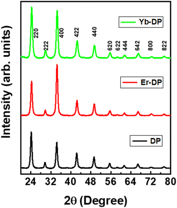 |
| | Fig. 1 X-ray diffraction (XRD) patterns of DP, Er-DP and Yb-DP. | |
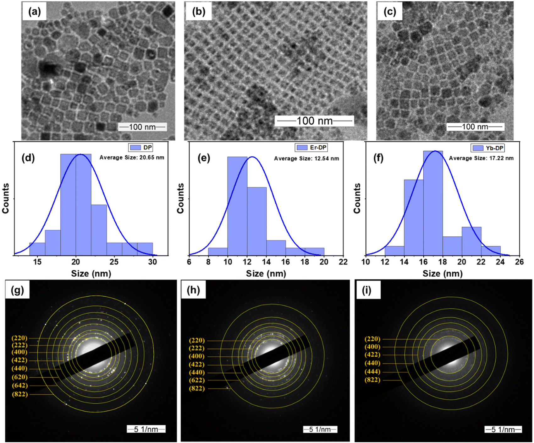
TEM images of DP, Er-DP and Yb-DP are shown in Fig. 2. In the TEM images, a highly crystalline cubic morphology was seen in both Er-doped and Yb-doped NCs [Fig. 2(b) and (c)]. The average size of the nanocrystals of undoped, Er-doped and Yb-doped perovskites are 20.65 nm, 12.54 nm and 17.22 nm, respectively [Fig. 2(d)–(f)]. The size distribution of the NCs narrowed in Er-DP and Yb-DP, which was consistent with earlier findings19 which showed that doping might have an impact on the NC size and uniformity. However, variations in the injection temperature at the time of synthesis also affect the size distribution of the NCs.1 The selected area electron diffraction (SAED) patterns of the corresponding NCs are shown in Fig. 2(g)–(i). The SAED pattern revealed the presence of the (220), (222), (400), (422), (440), (620), (642), (822) and (004) planes of the cubic phase in DP, confirming the formation of a consistent double perovskite structure. Moreover, the planes observed from the analysis of the SAED images of DP, Er-DP and Yb-DP are consistent with the XRD results. These structural investigations performed using TEM and SAED demonstrate that the perovskite NCs were produced from a pure phase without the occurrence of any structural transitions or traces of impurities.
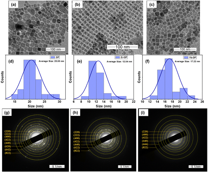 |
| | Fig. 2 Low magnification TEM images of (a) DP, (b) Er-DP and (c) Yb-DP. The average size of the corresponding NCs is shown in (d)–(f). SAED patterns of (g) DP, (h) Er-DP and (i) Yb-DP. | |
The UV-visible absorption spectra of all of these DPNC colloidal solutions are shown in Fig. S1(a)–(c), ESI,† which show the tails reaching close to 370 nm. Doping of Er or Yb introduces no new absorption bands. The absorptions were similar to those of previous reports,19,39 where parity-forbidden and parity-allowed transitions were observed for the transition from the valence band maxima to the conduction band minima. For the parity-allowed transition (strong transition) and the parity-forbidden transition (weak band edge transition), Tauc plots (Fig. S1(d)–(f), ESI†) were employed using (αhν)2versus hν and (αhν)2/3versus hν, where α is the absorbance coefficient, h is the Planck constant, and ν is the frequency of photons. The Cs2AgInCl6 double perovskite possesses a direct bandgap semiconductor12 and the optical bandgaps (weak band edge transition) determined by the Tauc plots were 3.32, 3.32 and 3.29 eV for DP, Er-DP and Yb-DP, respectively, and are in good agreement with other researchers’ observation.19,39,40 Our sample's absorption profiles are similar to that of Cu2O which exhibits strong peaks at higher energies and a weak band-edge tail at lower energy. For Cu2O, optical transitions from the direct and parity-forbidden band edge and subsequent higher-order parity-allowed states have been reported.41
Photoluminescence (PL) and PL excitation (PLE)
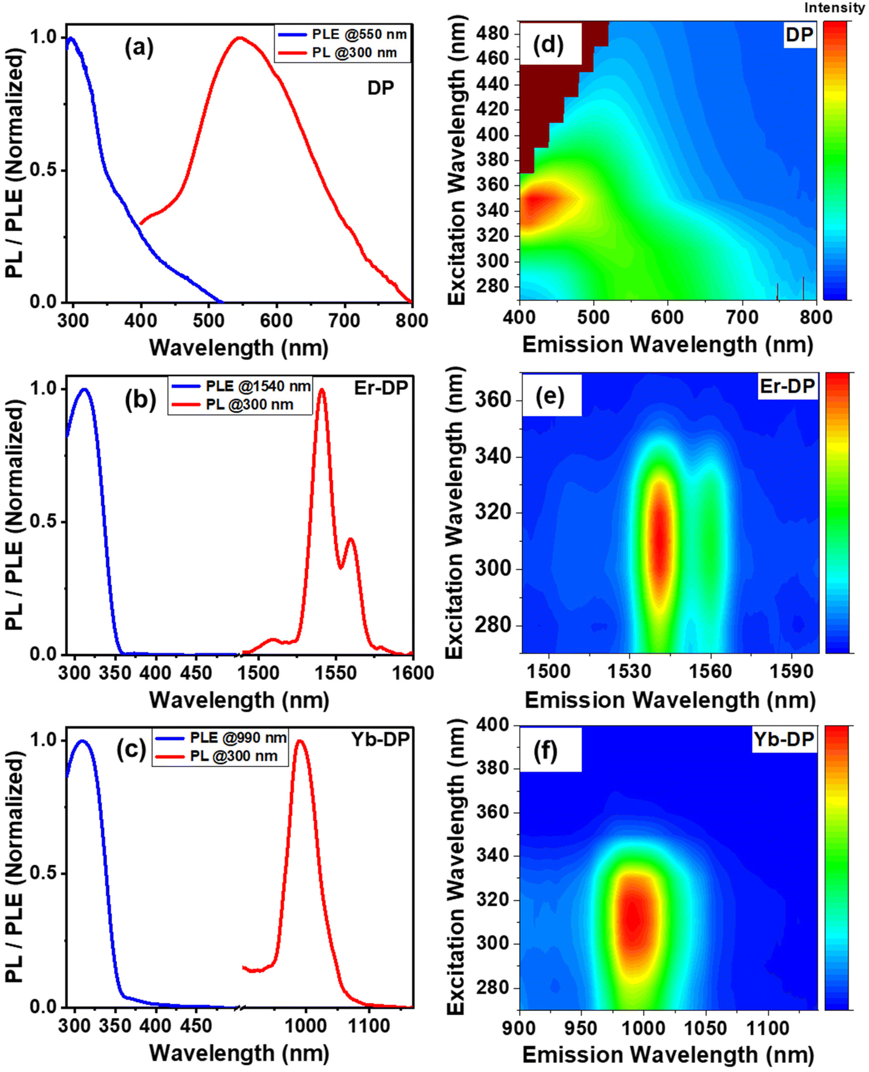
When DP was excited with a 300 nm wavelength light, it exhibited a broad emission, which has a peak at around 550 nm [Fig. 3(a)]. This PL was blue-shifted compared to those of previously reported bulk samples,40,42 which originates because of the small size of our NCs. A PL excitation (PLE) curve [Fig. 3(a)] was acquired at an emission wavelength of 550 nm to better comprehend the emission state. The PLE curve has a sharp peak near 300 nm associated with the band-edge absorption and a small hump at 375 nm, which can be assigned for the surface and/or defect-related states. We have also performed PLE measurements for different emission wavelengths from 500 to 700 nm [Fig. S4(a) and S4(d), ESI†]. The PLE spectra exhibit identical shapes with a small shift of peaks when changing the detection wavelengths, suggesting that the observed emission may arise from the radiative recombination from different excited states of similar kinds. We also notice variations in the PLE intensity, which should be due to the different absorption coefficients of DP for varied wavelengths.43
 |
| | Fig. 3 Photoluminescence (PL) curves at an excitation wavelength of 300 nm of (a) DP, (b) Er-DP and (c) Yb-DP. Photoluminescence excitation (PLE) curves at an emission wavelength of 550 nm for (a) DP, at an emission wavelength of 1450 nm for (b) Er-DP, and at an emission wavelength of 550 nm for (c) Yb-DP. Pseudo color plot between the excitation wavelength vs the emission wavelength at room temperature for (d) DP, (e) Er-DP and (f) Yb-DP. | |
Upon excitation at 300 nm, PL emission spectra (visible to near-infrared range) of Er-DP and Yb-DP were obtained, as shown in Fig. S5, ESI.† The visible region PL spectra showed similar characteristics as the PL emission of the host DP. Er-DP and Yb-DP showed a sharp PL band with a peak at 1540 nm and 990 nm, respectively, upon excitation at 300 nm, as shown in Fig. 3(b) and (c). There was no new absorption feature we noticed corresponding to this NIR PL. In order to inspect the source of this NIR emission, photoluminescence excitation spectra of Er-DP and Yb-DP were measured. The PLE spectra of Er-DP and Yb-DP [Fig. 3(b) and (c)] showed a strong peak at around 310 nm, which is attributed to the band-edge absorption. The PLE peak of the undoped sample was located at 300 nm while the PLE maxima of lanthanide-doped Cs2AgInCl6 NCs were found to be red-shifted. This may be attributed to the improved crystallinity of the doped NCs. Similarly, crystallinity improvement was observed for co-doping cerium and bismuth into the Cs2AgInCl6 nanocrystals.15 Unlike DP, Yb-DP and Er-DP only showed the peak for band-edge absorption and no defect states associated the peak near 375 nm were observed. Excitons trapped in the defective states in the NCs are thought to be incapable of transmitting energy to lanthanide dopants, resulting in the lack of the defective state PLE peak in the doped NCs. A similar observation was found in a previous report.19 The excited host transfers its energy to lanthanide dopants, exciting the f-electrons in the lanthanide material. The excited dopant Er undergoes f-band transition from 4I13/2 to 4I15/2, emitting near 1540 nm and Yb undergoes f–f deexcitation from 2F5/2 to 2F7/2, emitting near 990 nm. The results are in line with that of the previous report.19 We examined the PLE maps at different emission wavelengths for Er-DP [Fig. S4(b) and S4(e)†] and Yb-DP [Fig. S4(c) and S4(f)†] and found identical features of the PLE spectra, which agreed with the PL spectrum.
Furthermore, PL emission spectra of DP, Er-DP and Yb-DP were recorded at various excitation wavelengths as shown in Fig. 3(d)–(f) and Fig. S3, ESI.† For DP, the excitation energies play a significant role in the PL spectra; when the excitation wavelength was increased from 270 to 330 nm, the PL emission peaks shifted to lower wavelengths and when the excitation wavelength was increased from 340 to 330 nm, the PL emission peaks moved to higher wavelengths. [Fig. 3(d) and Fig. S3(a), ESI†]. These phenomena of excitation-dependent PL emission mapping may be due to the presence of several trap states, as observed for nanoparticles in previous reports.44–46 Therefore, the broadband emission appeared for the host DP originates from the recombination through different energy states. On the other hand, there are no significant changes in the excitation-dependent PL peak for Er-DP and Yb-DP represented in the pseudo color maps in Fig. 3(e) and (f). It is clear from the identical features of the PLE and PL spectra at various wavelengths that the emission results from the recombination of the same excited state, which is the f–f deexcitation of rare-earth materials.
Temperature-dependent PL study
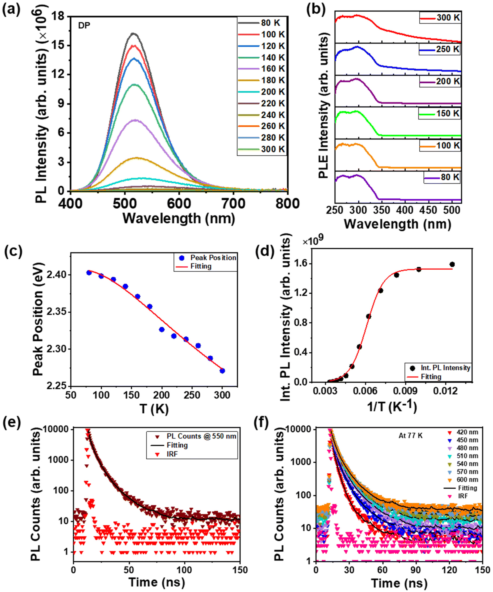
We conducted PL measurements of undoped and rare-earth-doped Cs2AgInCl6 NCs under an excitation wavelength of 300 nm at varying temperatures from 80 K to 300 K to understand the emission characteristics better. The temperature-dependent PL data of DP [Fig. 4(a)] describe the electron–phonon coupling properties. At low temperature, we observed several changes in the PL profile, including changes in the peak position, linewidth and intensity. Decreased phonon vibration and suppression of nonradiative recombination at a lower temperature may be a possible reason, as has been found in conventional semiconductors.47–50 We observed a red shift in the PL peaks with increasing temperature, as shown in Fig. 4(c). The PL peaks of conventional semiconductors depict a shift toward longer wavelengths while increasing temperature due to the lattice dilation and the electron–phonon interaction.51,52 The exciton dissociation with increasing temperature was the reason for the thermal quenching of the PL peaks. Additionally, we measured PLE spectra upon decreasing the temperature from 300 K to 80 K at an emission wavelength of 550 nm; the PLE peak position remained nearly constant [Fig. 4(b)]. The PL peak position shifted at longer wavelengths and the PLE peak position remained the same, resulting in an increased Stokes shift with increasing temperature. This increased Stokes shift may originate from the lattice contraction.
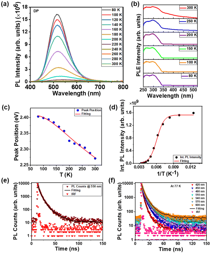 |
| | Fig. 4 Temperature-dependent (a) PL at an excitation wavelength of 300 nm, (b) PLE at an emission wavelength of 550 nm, (c) PL peak position and (d) integrated PL intensity. (c) and (d) are associated with (a). (e) Room temperature time-resolved PL (TRPL) at an emission wavelength of 550 nm measured by TCSPC; (f) wavelength-dependent TRPL at 77 K. All the figures are for DP. Open scattered symbols represent experimental data and solid lines show theoretical fittings. | |
To evaluate the activation energy, the integrated PL intensities were fitted as a function of temperature (T) [Fig. 4(d)] using the following Arrhenius equation:15
| |  | (1) |
where the activation energy of nonradiative transitions or the exciton dissociation process is denoted by
EA,
I0 is the int. PL intensity at 0 K,
A is defined as a pre-exponential constant factor calculated from the fitting of the temperature-dependent PL intensity and
kB is the Boltzmann constant. The activation energy,
EA, was found to be 0.13 eV. If there is no other nonradiative decay channel involved in the recombination of the exciton, the activation energy is thought of as the exciton binding energy (of STEs) in the halide perovskite NCs.
53,54 The exciton binding energy controls the equilibrium of exciton ionization and formation, which impacts the carrier density and charge transport. Exciton binding energy is a crucial aspect to understand the fabrication and operation of an optoelectronic device. The exciton–phonon coupling of Cs
2AgInCl
6 NCs in a film was studied by measuring the temperature dependence of PL linewidth broadening. The exciton–phonon interaction was responsible for the significant broadening of the linewidth for the inorganic perovskite NCs. The strength of electron–phonon coupling was evaluated in terms of the Huang–Rhys parameter (
S), which was calculated using the following equation:
14| | 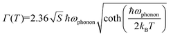 | (2) |
where
ħωphonon is the phonon frequency involved in the relaxation of band-edge excitation. The
S value for undoped Cs
2AgInCl
6 NCs was found to be 62.2 (Fig. S6, ESI
†), indicating the strong electron–phonon coupling, which is necessary for STE formation. We obtained
ħωphonon = 21 meV, which was compatible with previous reports of similar material systems. Luo
et al.14 reported a phonon frequency of 17.4 meV for bulk Cs
2AgInCl
6. A phonon frequency of 18.73 meV for Cs
3Cu
2I
5 NCs was reported by Lian
et al.55
To explore the PL decay dynamics of the STEs, we recorded time-resolved emission spectra (TRES) at room temperature and at a low temperature (77 K) for the NC thin film while excited with a 405 nm pulsed diode laser (picosecond) source. Time-resolved PL (TRPL) at an emission wavelength of 550 nm at room temperature is shown in Fig. 4(e), The TRES at 77 K is shown in Fig. 4(f) and the TRES at room temperature is shown in Fig. S7, ESI.† The PL decay profiles were fitted well by a triexponential function: I(t) = (a1![[thin space (1/6-em)]](https://www.rsc.org/images/entities/char_2009.gif) exp(−t/τ1) + a2exp(−t/τ2) + a1exp(−t/τ3)). The average PL decay times (τave) were obtained from the following expression: τave = ((a1 × τ12) + (a2 × τ22) + (a3 × τ32))/((a1 × τ1) + (a2 × τ2) + (a3 × τ3)). Here I(t) is the PL intensity at time t; τ1, τ2 and τ3 are the PL lifetime components; a1, a2 and a3 are the corresponding amplitudes. The fitting results and τave at different emission wavelengths are listed in Table S1 in the ESI.† The average PL lifetime of DP at an emission wavelength of 550 nm at room temperature was determined to be 5.59 ns. When the TRPL was taken from the blue to the red side of the emission curve (at 77 K), the PL transients gradually became slower from 420 to 540 nm [Fig. 4(f)]. The corresponding lifetimes at different emission wavelengths are listed in Table S2 in the ESI.† The increase in lifetime values for lower-energy locations indicates the emergence of STE states. These STE states were created by the interaction of excitons with surrounding lattices. The recombination through STE states is the source of the inhomogeneous distribution of photon energies, which broadened the PL emission spectrum. The crystal structure's larger lattice distortions led to the creation of deeper STE states.56 These deeper STEs take a longer time to recombine and emit photons with higher wavelengths. At the emission wavelengths of 570 and 600 nm, the average PL lifetime became slightly faster because at those wavelengths the PL emission intensity reduced. The PL emission for doped samples shown in Fig. S5, ESI,† is attributed as STE emission of the host associated with the Jahn–Teller distortion of the [AgCl6]5− octahedra. We found the same characteristics for this emission, including TRPL, for all the samples in the STE emission region.
exp(−t/τ1) + a2exp(−t/τ2) + a1exp(−t/τ3)). The average PL decay times (τave) were obtained from the following expression: τave = ((a1 × τ12) + (a2 × τ22) + (a3 × τ32))/((a1 × τ1) + (a2 × τ2) + (a3 × τ3)). Here I(t) is the PL intensity at time t; τ1, τ2 and τ3 are the PL lifetime components; a1, a2 and a3 are the corresponding amplitudes. The fitting results and τave at different emission wavelengths are listed in Table S1 in the ESI.† The average PL lifetime of DP at an emission wavelength of 550 nm at room temperature was determined to be 5.59 ns. When the TRPL was taken from the blue to the red side of the emission curve (at 77 K), the PL transients gradually became slower from 420 to 540 nm [Fig. 4(f)]. The corresponding lifetimes at different emission wavelengths are listed in Table S2 in the ESI.† The increase in lifetime values for lower-energy locations indicates the emergence of STE states. These STE states were created by the interaction of excitons with surrounding lattices. The recombination through STE states is the source of the inhomogeneous distribution of photon energies, which broadened the PL emission spectrum. The crystal structure's larger lattice distortions led to the creation of deeper STE states.56 These deeper STEs take a longer time to recombine and emit photons with higher wavelengths. At the emission wavelengths of 570 and 600 nm, the average PL lifetime became slightly faster because at those wavelengths the PL emission intensity reduced. The PL emission for doped samples shown in Fig. S5, ESI,† is attributed as STE emission of the host associated with the Jahn–Teller distortion of the [AgCl6]5− octahedra. We found the same characteristics for this emission, including TRPL, for all the samples in the STE emission region.
After summarizing all the optical characteristics of DP, including the broad PL spectrum, large Stokes shift, high value of the Huang–Rhys factor and large exciton binding energy, we infer that the emission of the Cs2AgInCl6 samples results from the STEs. There are several previous reports15,31,55,57 where we observed STE formation for DPNCs. Using a high-energy excitation, an electron transition occurs from the ground state (GS) to the excited states (ES) of DP and then the electron moves to the self-trapped states originating from excited-state structural reorganization. On the other hand, for lanthanide (Ln3+)-doped Cs2AgInCl6 NCs, energy transfer occurred from the ES of the host Cs2AgInCl6 to the f-states of rare-earth materials,58,59 and f–f transition emissions were observed.
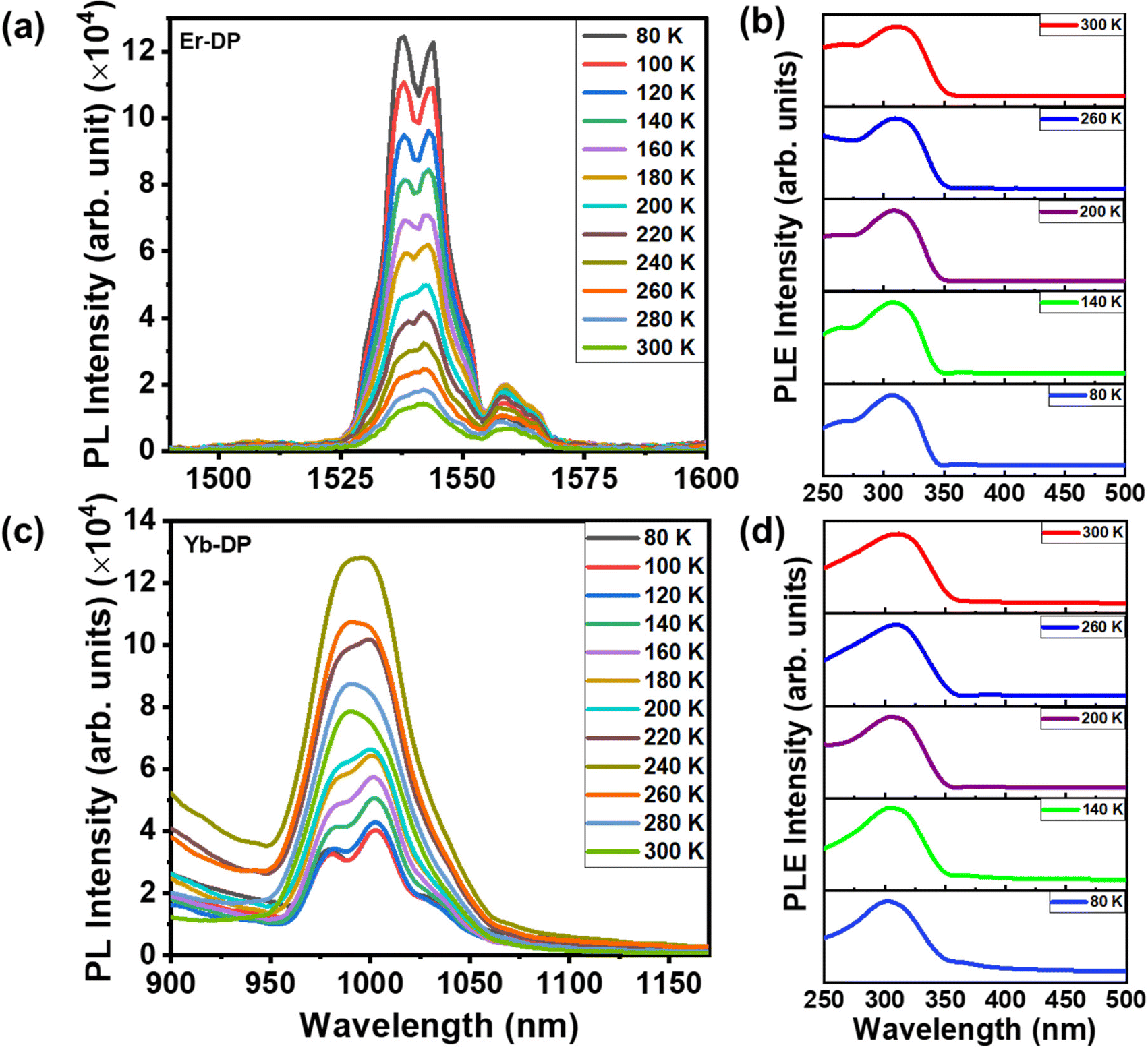
Fig. 5(a) shows temperature-dependent PL spectra of Er-DP, which exhibit a variety of characteristics at 300 K, including peaks at 1540 and 1560 nm. Due to the crystal-field-split manifold of the 4I13/2 and 4I15/2 states, such multiple PL peaks arise.60,61 Lower temperatures result in a more symmetric PL and the peak at 1560 disappears. Earlier reports of similar temperature-dependent Er3+ emission from other hosts that were doped with Er3+ were attributed to population redistribution among the crystal-field-split manifolds as a function of temperature.61 Also, as the temperature decreases, the PL intensity increases, which is explained by the fact that lower temperatures prevent nonradiative recombination,62 resulting in a higher PL intensity. Fig. S8 in the ESI† shows the integrated PL intensity at different temperatures in the range of 80 K–300 K, which describes the dependency of PL intensity on temperatures well. The temperature-dependent PLE in Er-DP [Fig. 5(b)] and Yb-DP [Fig. 5(d)] exhibits a negligible change in the peak positions and spectral shape, indicating a strong overlap of the related energy states.
 |
| | Fig. 5 Temperature-dependent (a) PL of Er-DP at an excitation wavelength of 300 nm and (b) PLE of Er-DP at an emission wavelength of 1540 nm. Temperature-dependent (c) PL of Yb-DP at an excitation of 300 nm and (d) PLE of Yb-DP at an emission wavelength of 990 nm. | |
We have further checked the variation of PL behavior as a function of temperature from 80 to 300 K for Yb-DP. At low temperature, Yb-DP exhibited two emission features at wavelengths of 980 and 1001 nm, as shown in Fig. 5(c). These peaks are assigned to the transitions of the splitting f-f sublevels. The emission intensity of upper sublevels initially increases with increasing temperature because a small energy difference between these sublevels allows electrons at a lower energy level to populate the upper level through the thermalization process.63,64 As a result, with increasing temperature, the intensity of the higher energy PL peak (around 980 nm at 80 K) increased. A similar temperature-dependent PL emission behavior was noticed for the Sb/Ho co-doped Cs2NaInCl6 double perovskite.65 Furthermore, a tiny red shift in the higher energy PL peak with increasing temperature was observed for Yb-DP. Increased phonon vibration and nonradiative recombination at higher temperatures may be the possible reasons.
Femtosecond Z-scan toward NLO applications
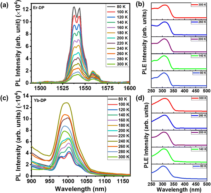
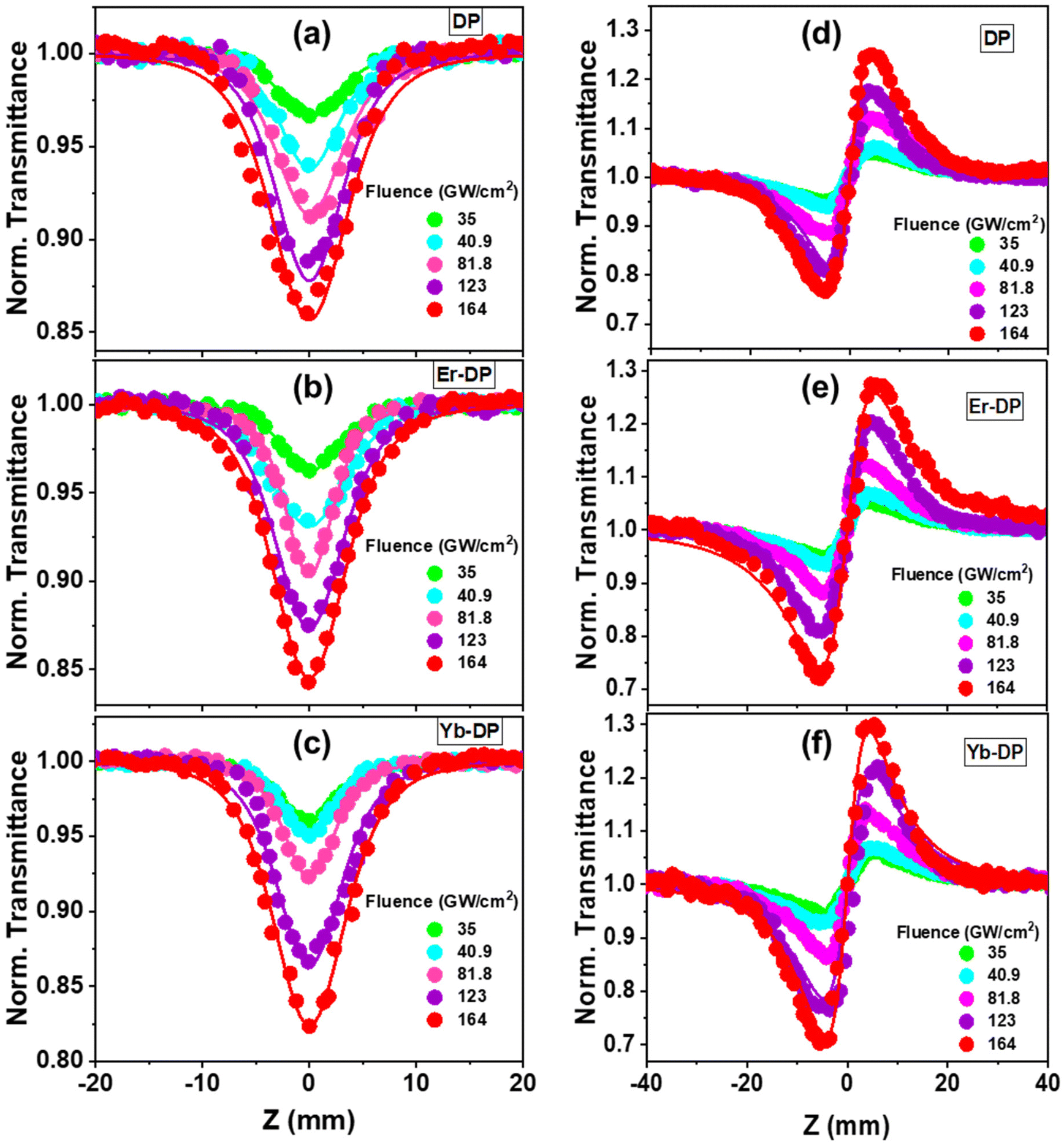
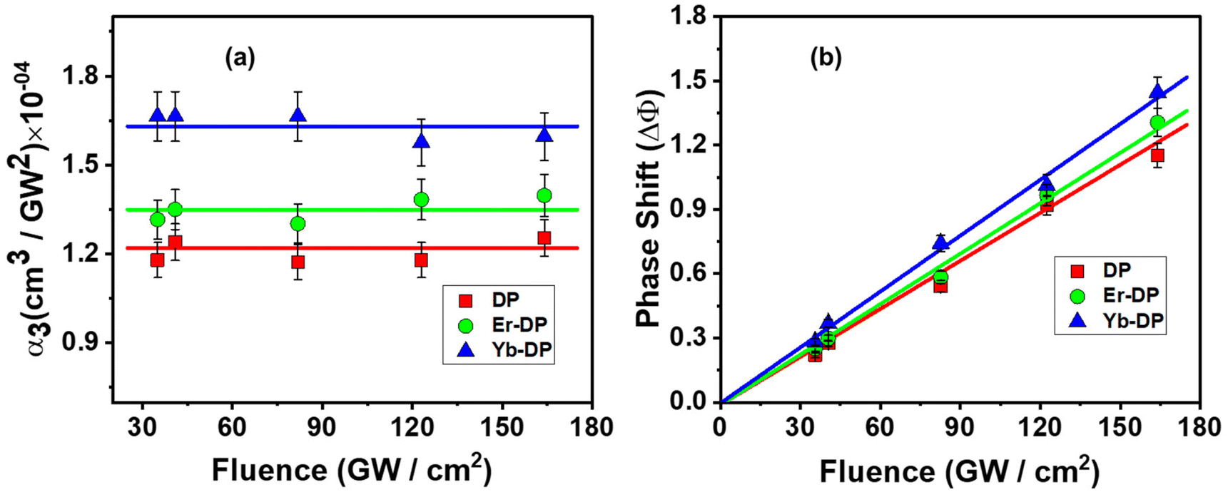
Halide perovskites have exhibited promising nonlinear optical properties, including the multiphoton absorption (MPA) effect.34,66 To realize the applications of lanthanide-doped Cs2AgInCl6 NCs as a potential nonlinear optical material, the fs Z-scan method was used, employing an 800 nm non-resonant excitation. These nanocrystals’ multiphoton absorption characteristics were ascertained using the open aperture (OA) Z-scan experiment, whereas their third-order nonlinear refractive index and second hyperpolarizability were calculated by using the closed aperture (CA) Z-scan experiment. Fig. 6 shows symmetric transmission plots of the fluence-dependent OA and CA Z-scan curves. The location of the sample is shown by the horizontal axis, and the sample's focus point is at Z = 0. The vertical axis represents the intensity of transmitted light which is normalized by the obtained light intensity at the far away points from focus (Z = 0) of each Z-scan where the excitation intensity is substantially very weak and the NLO effects are negligible. For the OA Z-scan data, the transmission through the sample reduced at the higher input beam intensities as the sample reached closer to the Z = 0 point. For all the samples, we found a reverse saturable absorption (RSA) kind of behaviour. A system will often have a strong RSA response if the excited-state absorption is higher than the ground-state absorption. While the RSA can result in a low absorption at low input intensities of the incident laser, it can also result in significant absorption by the nonlinear absorber67 at high input intensities of the incoming laser. For all of the DPNCs studied here with an 800 nm excitation wavelength, we observed (shown in Fig. S2, ESI†) minimal single-photon absorption. More specifically, given our experiment's circumstances, the direct electronic transition cannot be possible from the valence band to the conduction band with a single-photon absorption. Thus, the electrons can reach the conduction band via only MPA. At sufficiently high irradiances, the nonlinear response of a medium gives rise to multi-photon absorption. MPA is the simultaneous absorption of two or more photons, where the combined energy of the absorbed photons exceeds the energy bandgap of the medium. The number of photons that are simultaneously absorbed depends on the photon energy and the energy bandgap of the medium. For our material systems, nonlinear absorption processes like two-photon absorption (2PA) or three-photon absorption (3PA) may be anticipated. Using the transmitted equations [eqn (S2) and (S3), ESI†] for 2PA and 3PA, the OA Z-scan experimental data were fitted, and we obtained satisfactory fittings using the 3PA equation for all the NCs shown in Fig. 6(a)–(c). Additionally, the corresponding energy for 800 nm is 1.55 eV and thus the presence of 3PA absorption (with an energy of 4.65 eV) is sufficient for the transition of the population from the ground to the excited state (bandgap is ∼3.3 eV). Therefore, the superior mechanism for the observed RSA is 3PA. In Fig. 7(a), the obtained three-photon nonlinear absorption coefficient α3 is plotted against the input intensities. In this figure, the error bars indicate the maximum experimental errors of ∼10%. As shown in Fig. 7(a), α3 remained constant with increasing input intensities,68 clearly demonstrates that 3PA is involved in the nonlinear process that occurred here. We took the data up to 164 cm2 GW−1. The solvent started contributing to the nonlinear absorption part at an intensity higher than this fluence. The obtained values of the 3PA coefficient for DP, Er-DP and Yb-DP were 1.22 × 10⁻⁴ cm3 GW−2, 1.35 × 10⁻⁴ cm3 GW−2 and 1.64 × 10⁻⁴ cm3 GW−2, respectively. Besides, we have also calculated the three-photon absorption cross-section (σ3PA) using the equation σ3PA = α3(ħω)2/N, where the frequency of input laser beam is ω and N is the number density. The significant 3PA coefficients indicated that these NCs may be used for three-photon imaging (3PI).69 3PI provides better spatial confinement and helps to acquire higher resolutions and contrast in the imaging process, making it one of the most promising recent developments in multiphoton microscopy technology. Applications based on 3PA have also include 3PA-based optical limiting and three-photon-pumped lasers.70
 |
| | Fig. 6 Fluence-dependent OA Z-scan data of (a) DP, (b) Er-DP, and (c) Yb-DP; fluence-dependent CA Z-scan data of (d) DP, (e) Er-DP, and (f) Yb-DP. Scattered symbols represent experimental data while the solid lines are theoretical fittings. | |
 |
| | Fig. 7 Excitation-fluence dependences of (a) the three-photon absorption coefficient obtained from OA measurements and (b) the phase shift obtained from CA measurements. Scattered symbols represent experimental data while the solid lines are linear fits. | |
The input intensity-dependent CA Z-scan experimental data points were fitted using a commonly used equation [eqn (S4), ESI†] to obtain the nonlinear parameters. From the fittings, the values of the on-axis nonlinear phase shift at the focus (ΔΦ) were extracted. As the intense laser beam is present in the nonlinear medium, the nonlinear refractive (NLR) index (n2) comes into picture and it alters the refractive index of the medium.71 The following relationship72 exists between the nonlinear phase shift and the nonlinear refractive index:
where
k = 2π/
λ is the wave vector,
I0 is the peak intensity of the incident laser beam at the focus, and
Leff represents the effective path length inside the sample.
Fig. 6(d)–(f) show the valley–peak shapes of the CA data for all our examined NCs. In order to reduce the impact of MPA, CA divided by OA data were taken for the analysis of CA
Z-scan. From the CA
Z-scan data, we have observed the transmission minimum (valley) at the pre-focal part followed by a transmission maximum (peak) at the post-focal part which is evidence of the occurrence of the self-focusing process and a positive sign of
n2. We obtained the values of fluence-dependent Δ
Φ and noticed that Δ
Φ varied linearly with the excitation fluence
I0 [
Fig. 7(b)]. The third-order nonlinearity is definitely dominating, as shown by this experimentally observed linear relationship.
73 The obtained values of
n2 were 0.92 × 10
−15 cm
2 W
−1, 1.02 × 10
−15 cm
2 W
−1, and 1.15 × 10
−15 cm
2 W
−1, respectively, for DP, Er-DP and Yb-DP.
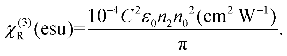
Additionally, we have calculated the third-order nonlinear susceptibility (χ(3)) using the values of n2. χ(3) is a complex quantity:74χ(3) = χR(3) + iχ(3)I, with the real portion (χ(3)R) related with n2 and the imaginary part (χ(3)I) associated with the 2PA coefficient.75 We estimates the real part of χ(3) using the following relationship:76
| | 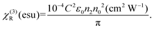 | (4) |
In the above equation, C represents the velocity of light, ε0 denotes the permittivity in free space and n0 is the linear refractive index of the sample. Because we didn't know the precise values of n0 for these samples, we chose n0 = 1.37, which is the linear refractive index of anhydrous hexane. We next estimated the second hyperpolarizability (〈γ〉) values of DPNCs77 using the obtained values of third-order NLO susceptibility. Eqn (S5)† was employed to determine 〈γ〉.78,79 The calculated values of 〈γ〉 for DP, Er-DP and Yb-DP were 5.26 × 10⁻³⁰ esu, 5.73 × 10⁻³⁰ esu and 6.46 × 10⁻³⁰ esu, respectively. Table 1 tabulates the estimated values of n2, χ(3)R, and 〈γ〉 for all the DPNCs investigated here. We noticed that the obtained NLO parameters are higher in the lanthanide-doped DPNCs than that in the host DPNCs. An enhancement of NLO parameters was observed not only for one parameter. All the NLO parameters were improved for the doped NCs. Therefore, we concluded that the change in the NLO properties is not due to sample variations; it is associated with the lanthanide doping. From the material characterization and with the support of a previous report,19 it was understood that lanthanide doping into Cs2AgInCl6 NCs improves their crystallinity. One can anticipate that improved crystallinity after doping is possibly one of the reasons for the enhanced nonlinearity.38,85–87 Crystalline materials have a more ordered arrangement of atoms, which typically leads to better NLO properties because the well-defined electronic states and energy levels of crystalline materials can interact more strongly with the electric field of the incident light pulse. Improved crystallinity can also enhance the third-order nonlinear susceptibility (χ(3)). These nonlinear susceptibilities describe the extent to which the material responds to the applied electric field and are key factors in determining the magnitude of the nonlinear optical effects. Other than the crystallinity, the nanocrystal size and semiconductor band gap may also affect the NLO characteristics. The highest value of the 3PA coefficient of Yb-DP can be explained by the inverse relationship between the nonlinear characteristics and semiconductor band gaps.88
Table 1 Obtained NLO parameters of the investigated DPNCs from OA and CA Z-scan studies
| Nonlinear parameters |
DP |
Er-DP |
Yb-DP |
|
α
3 (cm3 GW−2) × 10−4 |
1.22 |
1.35 |
1.64 |
|
σ
3PA (cm6 s2) × 10−75 |
2.50 |
2.77 |
3.34 |
|
n
2 (cm2 W−1) × 10−15 |
0.93 |
1.02 |
1.15 |
|
χ
(3)R (esu) × 10−14 |
4.49 |
4.88 |
5.51 |
| 〈γ〉 (esu) × 10−30 |
5.26 |
5.73 |
6.46 |
| Optical limiting onset (mJ cm−2) |
1.80 |
1.57 |
1.89 |
For evaluating the strength of nonlinear coefficients obtained for our samples, we compared them with those reported in the literature presented in Table 2. Gao et al.80 investigated the nonlinear optical properties of MAPbBr3 microplates for lasing application by employing a 100 fs, 1240 nm laser and obtained the value of α3 as 2.26 × 10⁻⁵ cm3 GW−2. This value of α3 is lower compared to ours. Li et al.81 determined a nonlinear refractive index value of −3.46 × 10⁻¹⁶ cm2 W−1 for the CsPb(Cl0.53Br0.47)3 NC solution by exciting with a 100 fs laser at a wavelength of 620 nm. Two-photon absorption for colloidal CsPbX3 perovskite nanocrystals (15–29 nm sizes) was reported by Liu et al.82 while using 396 fs pulses at 787 nm and a 1 kHz repetition rate and calculated the values of n2 as (4.7–6.8) × 10−15 cm2 W−1. 2PA also observed for CH3NH3PbCl3 single crystals73 by wavelength-dependent Z-scan measurements (180 fs, 660–840 nm) and reported n2 values of ∼10−15 cm2 W−1. Multiphoton absorption coefficients were reported in phase pure zero-dimensional Cs4PbBr6 perovskite films34 by applying a 70 fs, 500–1500 nm laser beam and obtained 3PA coefficients of (0.65–0.84) cm3 GW−2 and n2 values of ∼10−19 cm2 W−1. Recently, Mushtaq et al.30 determined n2 values of ∼10−13 cm2 W−1 for a Cs2AgIn0.9Bi0.1Cl6 NCs film by exciting with a 57 fs laser at a wavelength of 800 nm and they observed 2PA for these DPNCs. Krishnakanth et al.35 investigated the nonlinear properties of CsPbBr3 films of nanorods and nanocrystals and determined n2 values of ∼10−13 cm2 W−1 for the CsPbBr3 films of nanorods by applying a 70 fs, 600 nm laser beam with a peak intensity 40 × 1010 cm2 W−1. Evidently, these previously-reported NLO parameters were found to be comparable or even somewhat smaller in magnitude compared to the NLO parameters of our DPNCs. The previously reported higher-order NLO values are mostly for films or single crystals of perovskite materials. Also, most of them showed two-photon absorption. Additionally, we found that our obtained values of NLO parameters are better compared with those of organic compounds, which are known for good NLO responses.79,89–94 The values of the NLO parameters of DPNCs studied in this report are even one order higher than those of organic molecules.
Table 2 Comparison of the NLO coefficients with those of reported materials
| Material |
Laser parameters |
α
3 (cm3 GW−2) |
n
2 (cm2 W−1) |
Ref. |
| CH3NH3PbBr3 microstructures |
100 fs, 1240 nm |
2.26 × 10⁻⁵ |
— |
80
|
| CsPb(Cl0.53Br0.47)3 NCs |
100 fs, 620–720 nm |
— |
−10−16 |
81
|
| CsPbBr3 NCs |
396 fs, 787 nm |
— |
(4.7–6.8) × 10−15 |
82
|
| CH3NH3PbCl3 single crystals |
180 fs, 660–840 nm |
— |
∼10−14 |
73
|
| MAPbCl3 single crystals |
30 ps, 1064 nm |
0.05 ± 0.01 |
— |
83
|
| Cs4PbBr6 zero-dimensional perovskites |
70 fs, 500–1500 nm |
(0.65–0.84) |
∼10−9 |
34
|
| Cs2AgIn0.9Bi0.1Cl6 NC film |
57 fs, 800 nm |
— |
∼10−13 |
30
|
| MAPbBr3 nanospheres |
130 fs, 800 nm |
— |
–4.0 × 10⁻¹³ |
84
|
| CsPbBr3 nanorod film |
70 fs, 600 nm |
— |
6.5 × 10⁻¹³ |
35
|
| DP, Er-DP and Yb-DP |
70 fs, 800 nm |
(1.22–1.64) × 10−4 |
(0.93–1.15) × 10−15 |
Current work |
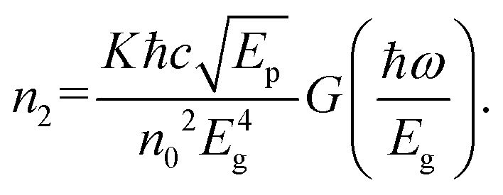
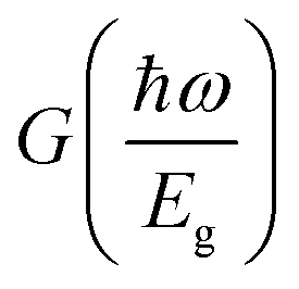
The Cs2AgInCl6 double perovskite is commonly well-known to possess a direct-gap band structure. Under the excitation of linearly polarized light, the band edge of Cs2AgInCl6 can be well approximated to an ideal nondegenerate direct-gap two-band model. For the nondegenerate two-band model, the NLR index n2 is related to the Kane energy Ep as:95
| | 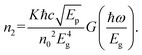 | (5) |
Eg is the band gap. The dispersion function

is a dimensionless function expressed as:
73| |  | (6) |
where
θ(
x) is the Heaviside step function demonstrated such that
θ(
x) = 0 for
x < 0 and
θ(
x) = 1 for
x ≥ 0.
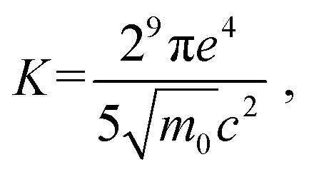
K is a material-independent constant,
95 written as:
| |  | (7) |
where
m0 is the free-electron mass. The value of
K is 1940 in units such that
n2 is in cm
2 GW
−1 and
Ep and
Eg are in eV.
95 The Kane energy
Ep is an important physical parameter, which is closely associated with the magnitude of the oscillator strength and
Ep describes the optical properties and electrical structures of a semiconductor material.
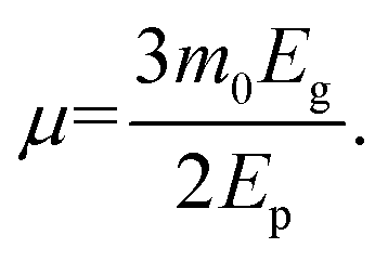
Eqn (8) provides the relationship between the reduced mass of exciton (
μ) and the Kane energy, which is expressed as:
96| |  | (8) |
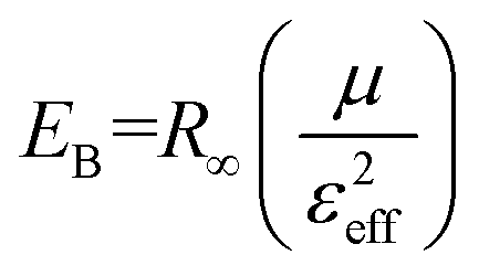
We used the obtained value of the NLR index n2 from eqn (5) to determine the value of Kane energy. Using eqn (8), the exciton reduced masses (μ) were calculated to 0.23m0, 0.20m0 and 0.19m0 for DP, Er-DP and Yb-DP, respectively. The estimated values of Ep and μ are listed in Table 3. Theoretically, the value of μ for Cs2AgInCl6 was estimated to be 0.23m0.97 Our obtained value of μ for undoped Cs2AgInCl6 is consistent with previously reported theoretical work. In this way, by analysing the closed-aperture Z-scan with the help of a two-band model we are able to estimate the value of μ, which is the fundamental physical parameter in perovskite materials. We have also noticed that rare-earth doping into the host Cs2AgInCl6 NCs reduced the exciton reduced mass. The smaller values of exciton reduced mass help to achieve the higher charge carrier mobility according to the Bardeen and Shockley's deformation potential model.98 The exciton binding energy EB is related to μ using the formula given by the Wannier–Mott model,99
| |  | (9) |
where
R∞ is the Rydberg constant and
εeff represents the effective dielectric constant.
EB is the difference between the energy of an exciton (electrons and holes are bounded by a screened Coulomb interaction) and the energy of an unbound non-interacting electron–hole pair. If we took
εeff = 3.77 from the previous theoretical report,
97 we estimated
EB = 0.23 eV. Therefore, from these analyses, it is possible to estimate the exciton binding energy also. By controlling the equilibrium of exciton formation, the exciton binding energy impacts the charge transport and carrier density, which are critical for device operation.
Table 3 Values of Ep and μ of DP, Er-DP and Yb-DP
| Material |
E
p (eV) |
μ (in terms of the rest mass of electrons m0) |
| DP |
21 |
0.23 |
| Er-DP |
25 |
0.20 |
| Yb-DP |
26 |
0.19 |
Optical limiting (OL) onset
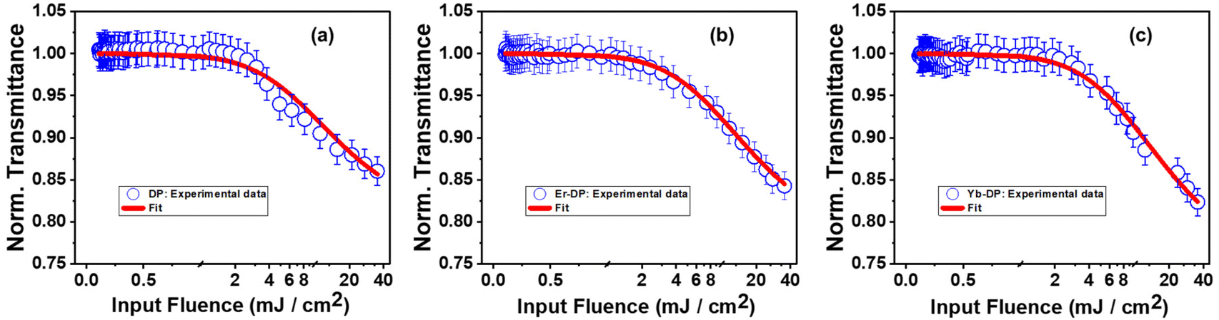
For these DPNCs, we calculated the onset of optical limiting (OL) and found that these nanocrystals can be applicable as a good optical limiter. An efficient optical limiter works as a transparent medium at low input intensities, and as an opaque medium at high input intensities. With the increase of input fluence, the transmittance of light through this kind of material diminishes. To maintain the intensity of transmitted light below a defined threshold, this phenomenon uses intensity-dependent transmission. Optical limiters are used for protecting the light-sensitive optical components, human eyes and the optical sensors from laser-induced damages.100 An effective optical limiter has a low limiting threshold, a high linear transmittance over the sensor spectrum, a high optical damage threshold and stability, a quick response time, and optical clarity. Different NLO processes, including MPA, excited-state absorption (ESA), free-carrier absorption (FCA), photo-refraction, nonlinear scattering, self-focusing, self-defocusing, etc., can lead to OL phenomena.101 In our situation, it was found that samples showed 3PA, which is what caused the OL presented here. Fig. 8(a)–(c) describe the variation of the normalized transmittance of light through the samples with respect to the incident laser fluence, which is acquired from the OA Z-scan data (at an incident peak intensity of 164 GW cm−2) using the following equation:100,102| |  | (10) |
where ω(z) represents the beam waist at each Z-point and Ein corresponds to the input laser pulse energy. The optical limiting onset value is the input fluence at which the normalized linear transmittance of the multiphoton-absorbing material deviates from the linearity.79,89Fig. 8 shows that for DP, Er-DP and Yb-DP, the deviation from linear transmittance occurred at an input fluence of 1.80 mJ cm−2, 1.57 mJ cm−2 and 1.89 mJ cm−2 respectively. The optical limiting onset values are presented in Table 4. These DPNCs may be applicable for optical limiting applications because they have lower optical limiting onset values.
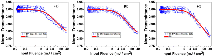 |
| | Fig. 8 Optical limiting onset curves of (a) DP, (b) Er-DP, and (c) Yb-DP. Open circular symbols represent experimental data and solid lines show theoretical fits. | |
Table 4 Comparison of optical limiting onset values
| Name of the material |
Laser pulse width, wavelength |
Optical limiting onset (J cm−2) |
Ref. |
| DP, Er-DP and Yb-DP |
70 fs, 800 nm |
1.80 × 10⁻³, 1.57 × 10⁻³, and 1.89 × 10⁻³ |
Current work |
| Cs2AgIn0.9Bi0.1Cl6 NC film |
57 fs, 800 nm |
(0.06–5.9) × 10−3 |
30
|
| CsPbBr3 NCs |
60 fs, 800 nm |
13.2 × 10⁻³ |
103
|
| CsPbI2Br NCs |
60 fs, 800 nm |
6.2 × 10⁻³ |
103
|
| Benzylamine lead(II) bromide perovskite microdisks |
68 fs, 800 nm |
1.2 × 10⁻³ |
104
|
The estimated values of the OL onset of these nanocrystals could be compared favourably to those of the previously reported samples. The value of optical limiting threshold reported by Pal et al.104 for 50% transmittance reduction was 25.4 mJ cm−2, and the optical limiting onset was 1.2 mJ cm−2. Recently, they obtained an optical limiting onset of 0.06–5.9×10⁻³ J cm−2 for a Cs2AgIn0.9Bi0.1Cl6 NC film by varying the input intensity by applying a 57 fs, 800 nm laser.30 CsPbI2Br and CsPbBr3 perovskite nanocrystals have a limiting threshold of 6.2 and 13.2 mJ cm−2, respectively.103 We further compared the OL onset values with the materials other than perovskites. We obtained a limiting onset of ∼4 mJ cm−2 for protein chromophores uGFPc by applying an 800 nm, 70 fs laser.89 Additionally, previously, we obtained a limiting onset of 5.8 mJ cm−2 and 5.7 mJ cm−2 for G1, G3 organic molecules,79 respectively, by applying the same laser for excitation. We obtained the values of the OL onset to be 6.4 mJ cm−2 and 5 mJ cm−2 for porphyrin molecules LG5 and LG6, respectively.90,105
Although a number of hybrids and all-inorganic halide perovskites have possessed strong OL characteristics, it is important to note that the degradation of these kinds of materials remains a crucial concern. The development of halide perovskites and their composites with exceptional optical and thermal stabilities is essential in the advancement of perovskite material-based optical limiting and optoelectronic applications.
Figure of merit
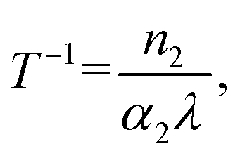
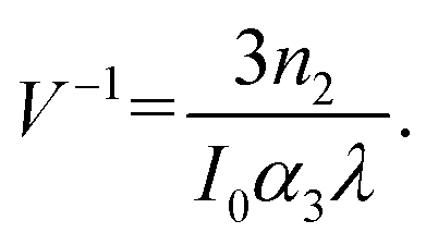
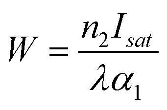
A convenient way to measure a system's effectiveness in terms of application is to calculate the figure of merit (FOM). We obtained the nonlinear FOM106,107 of these DPNCs to demonstrate their potential for photonic switching applications.108 Low nonlinear absorption and greater n2 are appropriate for optical switching applications. The FOM is associated with the maximum nonlinear phase shift. When the one-photon absorption is the dominant mechanism, the merit factor (W) or FOM is defined as108 , where Isat is the intensity of light at which the change of NLR index saturates, λ is the wavelength, α1 is the linear absorption coefficient and the absorption depth can be defined as α1−1. The nonlinear phase shift will be limited if nonlinear losses predominate in materials with potent multiphoton absorption. Then for the MPA, the absorption depth can be described as (I0α2)−1 and (I02α3)−1, where α2 and α3 are the 2PA and 3PA coefficients, respectively. The corresponding figures of merit (FOM) are defined as:
| |  | (11) |
| |  | (12) |
T < 1 and V < 0.68 are the conditions107,109 that must be satisfied to acquire a nominal nonlinear phase shift of 2π for switching and in order to operate properly a photonic device built of such materials.
In Fig. 9, we have shown the curves of the FOM with changing peak intensities in the 3PA region. We observed that the FOM is inversely proportional to the peak intensity and we also noticed that at an increment of 3PA (at lower peak intensities), the FOM decreased. Our calculated values of V by varying the peak intensities were 0.12–0.57 for DP, 0.12–0.58 for Er-DP and 0.13–0.61 for Yb-DP. It is noteworthy that the condition V < 0.68 is satisfied for all the DPNCs investigated here. For an input intensity of 230 GW cm−2, we reported the values of V as 0.57 and 0.59 for pc1 and pc2, respectively.108 Gu et al.109 reported the value of V as 0.64 for chalcone derivatives.
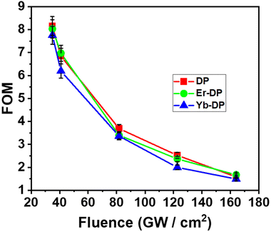 |
| | Fig. 9 Fluence-dependent FOM of DP, Er-DP and Yb-DP. Scattered symbols represent experimental data and solid and dotted lines are theoretical fittings. | |
Conclusions
A detailed investigation of the photophysical properties and femtosecond Z-scan studies toward ultrafast NLO applications of Cs2AgInCl6 NCs and lanthanide-doped Cs2AgInCl6 NCs is reported here. The XRD patterns of erbium and ytterbium-doped Cs2AgInCl6 NCs were found to be structurally identical to the XRD pattern of the host Cs2AgInCl6 NCs with the cubic phase and without any peak shifts, which confirmed the effective doping of the dopants into the host material without any unwanted peaks. The analysis of TEM images revealed that the size of all the DPNCs was in the nano-regime. The characteristic f–f transitions of NIR emission, which was tuned with Er-doping and Yb-doping in Cs2AgInCl6 NCs, might pave the way for several optoelectronic applications in light sources, displays, and communication networks. The excitation-dependent PL emission spectra of these DPNCs revealed the presence of several trap states in NCs. Temperature-dependent line broadening, thermal quenching of the PL emission, and a redshift of the PL peaks with increasing temperature were all found in the temperature-dependent PL emission spectra. We attributed this quenching of the PL peaks to exciton dissociation with increasing temperature. It was found that self-trapped excitonic emission was the reason for the broad PL spectra observed in the visible region. We fitted the temperature-dependent integrated PL intensities and calculated the exciton binding energy of STEs to be 0.13 eV. In NLO measurements, RSA characteristics were observed for the open aperture Z-scan data and 3PA coefficients were obtained for double perovskite materials for the first time at the excitation wavelength of 800 nm. The self-defocusing behavior of the samples was confirmed from the closed aperture Z-scan data. We estimated the values of second-hyperpolarizability to be (5.26–6.46) × 10−30 esu, which are greater than those of many recently reported materials. The fundamental physical parameters, Kane energy and exciton reduced mass, were calculated with the help of Z-scan data. We found that the obtained NLO coefficients are higher for lanthanide-doped DPNCs probably because of the increased crystallinity in Er-DP and Yb-DP. With the STE visible region emission, the NIR emission of rare-earth-doped NCs and various NLO applications, we believe that the multi-functionality of these potential material systems is revealed here and these DPNCs are potential candidates in the fabrication of photonic and nonlinear optoelectronic devices.
Experimental
Sample preparation
Cs2AgInCl6 NCs and lanthanide-doped Cs2AgInCl6 NCs were synthesized by the conventional hot injection method.1,19,39 The details of the synthesis method are described in the ESI.† We optimized and chose the doping level which gave the best results and was in accordance with the previous reports and continued with measuring the nonlinear optical properties. We synthesized DPNCs following the feed ratios of Yb/In = 20% for Yb-doped NC and Er/In = 20% for Er-doped NC as described in the literature.19 After synthesis, we prepared drop-casted films using quartz substrates from the colloidal solution of these double perovskite nanocrystals for the experiments in the film phase and prepared dilute solutions of a concentration of 0.05 mM using hexane solvent for the experiments in solution form.
XRD and TEM
Using a Rigaku SmartLab with Cu Kα radiation (λ = 1.5406 Å), powder X-ray diffraction (XRD) patterns of the film samples were captured. Transmission electron microscopy (TEM) images were collected using a transmission electron microscope (JEOL JEM-2100). Using ImageJ software, the size distribution of the NCs was approximated. With a 200 kV applied voltage, selected area electron diffraction (SAED) patterns were measured and they were used to examine the structural properties of these NCs.
UV-Visible absorption and photoluminescence (PL) measurements
UV-Visible absorption spectra of the solution samples were recorded using a commercial UV-Vis spectrometer. The PL and PLE spectra of the samples were recorded using an FLS 1000 (Edinburgh Instruments Ltd) fluorescence spectrometer. To study the time-resolved photoluminescence (TRPL) of the host Cs2AgInCl6 NCs, the standard time-correlated single-photon counting (TCSPC) method was employed. Low temperature PL of the nanocrystals was performed using the same spectrometer attached with an OptistatDN cryostat (a vacuum liquid nitrogen cryostat), and a Mercury iTC (Oxford Instruments) temperature controller was used to regulate the temperature. A xenon lamp was used to excite the samples, and an emission between 400 and 800 nm was collected. The drop-casted film samples were used for all the photoluminescence studies.
Femtosecond Z-scan (fs Z-scan) experiment
A standard Z-scan setup68,79,90,110 was used to conduct fs Z-scan experiments. The light source was a Ti: sapphire laser amplifier (LIBRA, M/S Coherent) seeded with an oscillator (Chameleon). A part of the amplifier's laser output with a central wavelength of 800 nm, a pulse duration of ∼70 fs, and a repetition rate of 1 kHz was used for the measurements. The laser beam was focused onto the sample using a plano-convex lens with a focal length of around 15 cm. The samples with a concentration of 0.05 mM were inserted in a 1 mm path length quartz cuvette, and with the aid of a sample holder, the cuvette was then vertically kept above the motorized stage. The samples were scanned to the positive and negative sides of the Z = 0 position by moving the stage in the Z-direction. In order to record the signal that was passed through the samples, a lock-In amplifier was connected to a silicon photodiode (PD-Thorlabs). The motorized stage was controlled by a motion stage controller (Newport-ESP 300) interfaced with LabVIEW software. The MPA of the samples can be determined by scanning the samples along the focal plane of the lens without placing an aperture in front of the photodiode. For the closed aperture Z-scan experiment, an aperture was placed at a far field prior to the photodiode for making the transmitted beam sensitive to the center area of the transmitted beam profile. Important properties like the third-order nonlinear susceptibility (χ(3)) and nonlinear refractive index (n2) and second hyperpolarizability were calculated using the CA Z-scan study. To keep the contribution of the solvent negligible to the measured NLO properties, we have optimized the peak intensity of the incident laser on the samples. This was validated by the Z-scan measurement of pure solvent, which revealed insignificant NLO transmittance. In the Z-scan measurement, taking into consideration of stage backlash, estimation of intensity as a function of position of sample (Z) and fluctuations with the input laser, a maximum experimental error of about 10% was estimated.
Conflicts of interest
There are no conflicts to declare.
Acknowledgements
Dr S. S. K. Raavi acknowledges the financial support of the DST India (CRG/2019/003197) and DAE-BRNS (58/14/06/2023-BRNS/37030). D. B. acknowledges the funding support from PMRF. Prof. V. R. Soma thanks DRDO, India for the financial support through ACRHEM [ERIP/ER/1501138/M/01/319/D (R&D)].
References
- F. Locardi, M. Cirignano, D. Baranov, Z. Dang, M. Prato, F. Drago, M. Ferretti, V. Pinchetti, M. Fanciulli and S. Brovelli, J. Am. Chem. Soc., 2018, 140, 12989–12995 CrossRef CAS PubMed.
- M. M. Yao, L. Wang, J. S. Yao, K. H. Wang, C. Chen, B. S. Zhu, J. N. Yang, J. J. Wang, W. P. Xu and Q. Zhang, Adv. Opt. Mater., 2020, 8, 1901919 CrossRef CAS.
- B. Yang, F. Hong, J. Chen, Y. Tang, L. Yang, Y. Sang, X. Xia, J. Guo, H. He and S. Yang, Angew. Chem., 2019, 131, 2300–2305 CrossRef.
- Y. Liu, Y. Jing, J. Zhao, Q. Liu and Z. Xia, Chem. Mater., 2019, 31, 3333–3339 CrossRef CAS.
- F. Locardi, E. Sartori, J. Buha, J. Zito, M. Prato, V. Pinchetti, M. L. Zaffalon, M. Ferretti, S. Brovelli and I. Infante, ACS Energy Lett., 2019, 4, 1976–1982 CrossRef CAS.
- J. C. Dahl, W. T. Osowiecki, Y. Cai, J. K. Swabeck, Y. Bekenstein, M. Asta, E. M. Chan and A. P. Alivisatos, Chem. Mater., 2019, 31, 3134–3143 CrossRef CAS.
- H. Bhatia, B. Ghosh and E. Debroye, J. Mater. Chem. C, 2022, 10, 13437–13461 RSC.
- Y. Wei, Z. Cheng and J. Lin, Chem. Soc. Rev., 2019, 48, 310–350 RSC.
- S. Ghosh and B. Pradhan, ChemNanoMat, 2019, 5, 300–312 CrossRef CAS.
- Q. Fan, G. V. Biesold-McGee, J. Ma, Q. Xu, S. Pan, J. Peng and Z. Lin, Angew. Chem., Int. Ed., 2020, 59, 1030–1046 CrossRef CAS PubMed.
- A. Bibi, I. Lee, Y. Nah, O. Allam, H. Kim, L. N. Quan, J. Tang, A. Walsh, S. S. Jang and E. H. Sargent, Mater. Today, 2021, 49, 123–144 CrossRef CAS.
- G. Volonakis, A. A. Haghighirad, R. L. Milot, W. H. Sio, M. R. Filip, B. Wenger, M. B. Johnston, L. M. Herz, H. J. Snaith and F. Giustino, J. Phys. Chem. Lett., 2017, 8, 772–778 CrossRef CAS PubMed.
- Y. Liu, A. Nag, L. Manna and Z. Xia, Angew. Chem., 2021, 133, 11696–11707 CrossRef.
- J. Luo, X. Wang, S. Li, J. Liu, Y. Guo, G. Niu, L. Yao, Y. Fu, L. Gao and Q. Dong, Nature, 2018, 563, 541–545 CrossRef CAS PubMed.
- S. Wang, J. Qi, S. V. Kershaw and A. L. Rogach, ACS Nanosci. Au, 2021, 2, 93–101 CrossRef.
- M. Shang, C. Li and J. Lin, Chem. Soc. Rev., 2014, 43, 1372–1386 RSC.
- F. Wang and X. Liu, Chem. Soc. Rev., 2009, 38, 976–989 RSC.
- G. Pan, X. Bai, D. Yang, X. Chen, P. Jing, S. Qu, L. Zhang, D. Zhou, J. Zhu and W. Xu, Nano Lett., 2017, 17, 8005–8011 CrossRef CAS PubMed.
- W. Lee, S. Hong and S. Kim, J. Phys. Chem. C, 2019, 123, 2665–2672 CrossRef CAS.
- Y. Song, Y. Chen, X. Jiang, Y. Ge, Y. Wang, K. You, K. Wang, J. Zheng, J. Ji and Y. Zhang, Adv. Opt. Mater., 2019, 7, 1801777 CrossRef.
- A. Nayak, J. Park, K. De Mey, X. Hu, T. V. Duncan, D. N. Beratan, K. Clays and M. J. Therien, ACS Cent. Sci., 2016, 2, 954–966 CrossRef CAS PubMed.
- W. Ye, F. Zeuner, X. Li, B. Reineke, S. He, C.-W. Qiu, J. Liu, Y. Wang, S. Zhang and T. Zentgraf, Nat. Commun., 2016, 7, 1–7 Search PubMed.
- T. He, J. Li, X. Qiu, S. Xiao, C. Yin and X. Lin, Adv. Opt. Mater., 2018, 6, 1800843 CrossRef.
- Y. Mu, Z. He, K. Wang, X. Pi and S. Zhou, iScience, 2022, 25, 105371 CrossRef CAS PubMed.
- J. Zhang, X. Shen, S. Ma, J. Sun, F. Chen, H. Ma, L. An and K. Pan, Opt. Mater., 2023, 136, 113362 CrossRef CAS.
- H. Yu, J. Liu, J. Wang, J. Liu, H. Xu, J. Yu and W. Wu, J. Alloys Compd., 2023, 168742 CrossRef CAS.
- H. Tahara, T. Aharen, A. Wakamiya and Y. Kanemitsu, Adv. Opt. Mater., 2018, 6, 1701366 CrossRef.
- G. Xing, N. Mathews, S. S. Lim, N. Yantara, X. Liu, D. Sabba, M. Grätzel, S. Mhaisalkar and T. C. Sum, Nat. Mater., 2014, 13, 476–480 CrossRef CAS PubMed.
- H. Hirori, P. Xia, Y. Shinohara, T. Otobe, Y. Sanari, H. Tahara, N. Ishii, J. Itatani, K. L. Ishikawa and T. Aharen, APL Mater., 2019, 7, 041107 CrossRef.
- A. Mushtaq, B. Pradhan, D. Kushavah, Y. Zhang, M. Wolf, N. Schrenker, E. Fron, S. Bals, J. Hofkens and E. Debroye, ACS Photonics, 2021, 8, 3365–3374 CrossRef CAS.
- Y. Zhang, Q. Wang, N. Sui, Z. Kang, X. Li, H.-z. Zhang, J. Zhang and Y. Wang, Appl. Phys. Lett., 2021, 119, 161904 CrossRef CAS.
- Y. Zhang, N. Sui, Z. Kang, X. Meng, L. Yuan, X. Li, H.-z. Zhang, J. Zhang and Y. Wang, J. Mater. Chem. C, 2022, 10, 5526–5533 RSC.
- S. J. Khanam, D. Banerjee, V. R. Soma and B. Murali, J. Mater. Chem. C, 2023, 11, 3275–3283 RSC.
- K. Krishnakanth, S. Seth, A. Samanta and S. V. Rao, Nanoscale, 2019, 11, 945–954 RSC.
- K. N. Krishnakanth, S. Seth, A. Samanta and S. V. Rao, Opt. Lett., 2018, 43, 603–606 CrossRef CAS PubMed.
- I. Fuks-Janczarek, R. Miedzinski, L. Kassab and C. Bordon, Opt. Mater., 2020, 102, 109794 CrossRef CAS.
- M. Fu, P. Tamarat, H. Huang, J. Even, A. L. Rogach and B. Lounis, Nano Lett., 2017, 17, 2895–2901 CrossRef CAS PubMed.
- A. H. Yuwono, B. Liu, J. Xue, J. Wang, H. I. Elim, W. Ji, Y. Li and T. J. White, J. Mater. Chem., 2004, 14, 2978–2987 RSC.
- Y. Mahor, W. J. Mir and A. Nag, J. Phys. Chem. C, 2019, 123, 15787–15793 CrossRef CAS.
- J. Zhou, Z. Xia, M. S. Molokeev, X. Zhang, D. Peng and Q. Liu, J. Mater. Chem. A, 2017, 5, 15031–15037 RSC.
- S. Dolai, S. Das, S. Hussain, R. Bhar and A. Pal, Vacuum, 2017, 141, 296–306 CrossRef CAS.
- J. Luo, S. Li, H. Wu, Y. Zhou, Y. Li, J. Liu, J. Li, K. Li, F. Yi and G. Niu, ACS Photonics, 2018, 5, 398–405 CrossRef CAS.
- Y.-P. Lin, S. Hu, B. Xia, K.-Q. Fan, L.-K. Gong, J.-T. Kong, X.-Y. Huang, Z. Xiao and K.-Z. Du, J. Phys. Chem. Lett., 2019, 10, 5219–5225 CrossRef CAS PubMed.
- V. Štengl and J. Henych, Nanoscale, 2013, 5, 3387–3394 RSC.
- L. Bao, Z. L. Zhang, Z. Q. Tian, L. Zhang, C. Liu, Y. Lin, B. Qi and D. W. Pang, Adv. Mater., 2011, 23, 5801–5806 CrossRef CAS PubMed.
- B. Li, L. Jiang, X. Li, P. Ran, P. Zuo, A. Wang, L. Qu, Y. Zhao, Z. Cheng and Y. Lu, Sci. Rep., 2017, 7, 1–12 CrossRef PubMed.
- B. Chon, J. Bang, J. Park, C. Jeong, J. H. Choi, J.-B. Lee, T. Joo and S. Kim, J. Phys. Chem. C, 2011, 115, 436–442 CrossRef CAS.
- J. Li, X. Yuan, P. Jing, J. Li, M. Wei, J. Hua, J. Zhao and L. Tian, RSC Adv., 2016, 6, 78311–78316 RSC.
- D. Valerini, A. Creti, M. Lomascolo, L. Manna, R. Cingolani and M. Anni, Phys. Rev. B: Condens. Matter Mater. Phys., 2005, 71, 235409 CrossRef.
- G. Morello, M. De Giorgi, S. Kudera, L. Manna, R. Cingolani and M. Anni, J. Phys. Chem. C, 2007, 111, 5846–5849 CrossRef CAS.
- J. Wu, W. Walukiewicz, K. Yu, J. Ager III, E. Haller, H. Lu, W. J. Schaff, Y. Saito and Y. Nanishi, Appl. Phys. Lett., 2002, 80, 3967–3969 CrossRef CAS.
- P. Dey, J. Paul, J. Bylsma, D. Karaiskaj, J. Luther, M. Beard and A. Romero, Solid State Commun., 2013, 165, 49–54 CrossRef CAS.
- K. Wu, A. Bera, C. Ma, Y. Du, Y. Yang, L. Li and T. Wu, Phys. Chem. Chem. Phys., 2014, 16, 22476–22481 RSC.
- F. Zhang, H. Zhong, C. Chen, X.-g. Wu, X. Hu, H. Huang, J. Han, B. Zou and Y. Dong, ACS Nano, 2015, 9, 4533–4542 CrossRef CAS PubMed.
- L. Lian, M. Zheng, W. Zhang, L. Yin, X. Du, P. Zhang, X. Zhang, J. Gao, D. Zhang and L. Gao, Adv. Sci., 2020, 7, 2000195 CrossRef CAS PubMed.
- S. Bhaumik, ACS Omega, 2020, 5, 22299–22304 CrossRef CAS PubMed.
- Y. Liu, X. Rong, M. Li, M. S. Molokeev, J. Zhao and Z. Xia, Angew. Chem., Int. Ed., 2020, 59, 11634–11640 CrossRef CAS PubMed.
- L. Zhang and M. Yuan, Light: Sci. Appl., 2022, 11, 99 CrossRef CAS PubMed.
- S. Jin, R. Li, H. Huang, N. Jiang, J. Lin, S. Wang, Y. Zheng, X. Chen and D. Chen, Light: Sci. Appl., 2022, 11, 52 CrossRef CAS.
- H. Przybylinska, W. Jantsch, Y. Suprun-Belevitch, M. Stepikhova, L. Palmetshofer and G. Hendorfer, Phys. Rev. B: Condens. Matter Mater. Phys., 1996, 54, 2532 CrossRef CAS PubMed.
- Z. Ivanova, Z. Aneva, R. Ganesan, D. Tonchev, E. Gopal, K. Rao, T. Allen, R. DeCorby and S. Kasap, J. Non-Cryst. Solids, 2007, 353, 1418–1421 CrossRef CAS.
- C. Zhou, H. Lin, Y. Tian, Z. Yuan, R. Clark, B. Chen, L. J. van de Burgt, J. C. Wang, Y. Zhou and K. Hanson, Chem. Sci., 2018, 9, 586–593 RSC.
- Y. Shang, Q. Han, S. Hao, T. Chen, Y. Zhu, Z. Wang and C. Yang, ACS Appl. Mater. Interfaces, 2019, 11, 42455–42461 CrossRef CAS PubMed.
- Y. Zhao, D. Peng, G. Bai, Y. Huang, S. Xu and J. Hao, Adv. Funct. Mater., 2021, 31, 2010265 CrossRef CAS.
- J. Nie, H. Li, S. Fang, B. Zhou, Z. Liu, F. Chen, Y. Wang and Y. Shi, Cell Rep. Phys. Sci., 2022, 3, 100820 CrossRef CAS.
-
J. Jiang, G. Niu, L. Sui, X. Wang, X. Zeng, Y. Zhang, L. Che, G. Wu, K. Yuan and X. Yang, Adv. Opt. Mater., 2202634 Search PubMed.
-
S. V. Rao, K. N. Krishnakanth, C. Indumathi and T. S. Girisun, Handbook of Laser Technology and Applications: Lasers Applications: Materials Processing and Spectroscopy (Volume Three), 2021, vol. 3, pp. 255 Search PubMed.
- R. S. S. Kumar, S. V. Rao, L. Giribabu and D. N. Rao, Chem. Phys. Lett., 2007, 447, 274–278 CrossRef CAS.
- N. G. Horton, K. Wang, D. Kobat, C. G. Clark, F. W. Wise, C. B. Schaffer and C. Xu, Nat. Photonics, 2013, 7, 205–209 CrossRef CAS PubMed.
- Q. Zheng, G. S. He, C. Lu and P. N. Prasad, J. Mater. Chem., 2005, 15, 3488–3493 RSC.
- M. S. Ahmed, C. Biswas, P. B. Miranda and S. S. K. Raavi, Eur. Phys. J.: Spec. Top., 2021, 1–17 Search PubMed.
- S. K. Nayak, R. Kore, M. S. Ahmed, P. Verma, R. Vallavoju, D. Banerjee, S. Pola, V. R. Soma, P. Chetti and S. S. K. Raavi, Opt. Mater., 2023, 137, 113603 CrossRef CAS.
- K. Ohara, T. Yamada, H. Tahara, T. Aharen, H. Hirori, H. Suzuura and Y. Kanemitsu, Phys. Rev. Mater., 2019, 3, 111601 CrossRef CAS.
-
R. W. Boyd, Nonlinear optics, Academic press, 2020 Search PubMed.
- M. Sheik-Bahae, A. A. Said, T.-H. Wei, D. J. Hagan and E. W. Van Stryland, IEEE J. Quantum Electron., 1990, 26, 760–769 CrossRef CAS.
- A. Ekbote, P. Patil, S. R. Maidur, T. S. Chia and C. K. Quah, Dyes Pigm., 2017, 139, 720–729 CrossRef CAS.
- C. Biswas, K. Krishnakanth, J. Lade, A. Chaskar, A. Tripathi, P. Chetti, V. R. Soma and S. S. K. Raavi, Chem. Phys. Lett., 2019, 730, 638–642 CrossRef CAS.
- S. V. Rao, N. N. Srinivas, D. N. Rao, L. Giribabu, B. G. Maiya, R. Philip and G. R. Kumar, Opt. Commun., 2000, 182, 255–264 CrossRef CAS.
- C. Biswas, N. K. Katturi, N. Duvva, L. Giribabu, V. R. Soma and S. S. K. Raavi, J. Phys. Chem. C, 2020, 124, 24039–24051 CrossRef CAS.
- Y. Gao, S. Wang, C. Huang, N. Yi, K. Wang, S. Xiao and Q. Song, Sci. Rep., 2017, 7, 1–6 CrossRef PubMed.
- J. Li, C. Ren, X. Qiu, X. Lin, R. Chen, C. Yin and T. He, Photonics Res., 2018, 6, 554–559 CrossRef CAS.
- S. Liu, G. Chen, Y. Huang, S. Lin, Y. Zhang, M. He, W. Xiang and X. Liang, J. Alloys Compd., 2017, 724, 889–896 CrossRef CAS.
- F. O. Saouma, D. Y. Park, S. H. Kim, M. S. Jeong and J. I. Jang, Chem. Mater., 2017, 29, 6876–6882 CrossRef CAS.
- W. G. Lu, C. Chen, D. Han, L. Yao, J. Han, H. Zhong and Y. Wang, Adv. Opt. Mater., 2016, 4, 1732–1737 CrossRef CAS.
- M. Feng, H. Zhan and Y. Chen, Appl. Phys. Lett., 2010, 96, 033107 CrossRef.
- C. Quan, X. Xing, S. Huang, M. Jin, T. Shi, Z. Zhang, W. Xiang, Z. Wang and Y. Leng, Photonics Res., 2021, 9, 1767–1774 CrossRef.
- C. Redondo-Obispo, I. Suárez, S. J. Quesada, T. S. Ripolles, J. P. Martínez-Pastor, A. L. álvarez, A. de Andrés and C. Coya, J. Phys. Chem. Lett., 2020, 11, 2188–2194 CrossRef CAS PubMed.
- Y. Xie, J. Fan, C. Liu, S. Chi, Z. Wang, H. Yu, H. Zhang, Y. Mai and J. Wang, Adv. Opt. Mater., 2018, 6, 1700819 CrossRef.
- M. S. Ahmed, C. Biswas, D. Banerjee, P. Chetti, J.-S. Yang, V. R. Soma and S. S. K. Raavi, Front. Phys., 2022, 10, 549, DOI:10.3389/fphy.2022.914135.
- C. Biswas, S. G. Palivela, L. Giribabu, V. R. Soma and S. S. K. Raavi, Opt. Mater., 2022, 127, 112232 CrossRef CAS.
- S. Bhattacharya, C. Biswas, S. S. K. Raavi, J. Venkata Suman Krishna, N. Vamsi Krishna, L. Giribabu and V. R. Soma, J. Phys. Chem. C, 2019, 123, 11118–11133 CrossRef CAS.
- S. Bhattacharya, C. Biswas, S. S. K. Raavi, J. V. S. Krishna, D. Koteshwar, L. Giribabu and S. V. Rao, RSC Adv., 2019, 9, 36726–36741 RSC.
- Y.-D. Zhang, Z.-Y. Zhao, C.-B. Yao, L. Yang, J. Li and P. Yuan, Opt. Laser Technol., 2014, 58, 207–214 CrossRef CAS.
- M. S. Ahmed, C. Biswas, B. Bhavani, S. Prasanthkumar, D. Banerjee, V. Kumar, P. Chetti, L. Giribabu, V. R. Soma and S. S. K. Raavi, J. Photochem. Photobiol., A, 2023, 435, 114324 CrossRef CAS.
- M. S. Bahae, D. Hutchings, D. Hagan and E. Van Stryland, IEEE J. Quantum Electron., 1991, 27, 1296–1309 CrossRef.
- P. C. Sercel, J. L. Lyons, N. Bernstein and A. L. Efros, J. Chem. Phys., 2019, 151, 234106 CrossRef.
- M. Jain, P. Bhumla, M. Kumar and S. Bhattacharya, J. Phys. Chem. C, 2022, 126, 6753–6760 CrossRef CAS.
- J. Bardeen and W. Shockley, Phys. Rev., 1950, 80, 72 CrossRef CAS.
- M. J. Waters, D. Hashemi and J. Kieffer, Mater. Sci. Eng. B, 2020, 261, 114657 CrossRef CAS.
- P. Patil, S. R. Maidur, S. V. Rao and S. Dharmaprakash, Opt. Laser Technol., 2016, 81, 70–76 CrossRef CAS.
- S. V. Rao, P. T. Anusha, T. S. Prashant, D. Swain and S. P. Tewari, Mater. Sci. Appl., 2011, 2, 299 CAS.
-
R. L. Sutherland, Handbook of nonlinear optics, CRC press, 2003 Search PubMed.
- K. S. Rao, R. A. Ganeev, K. Zhang, Y. Fu, G. S. Boltaev, S. K. Maurya and C. Guo, Opt. Mater., 2019, 92, 366–372 CrossRef CAS.
- A. Mushtaq, D. Kushavah, S. Ghosh and S. K. Pal, Appl. Phys. Lett., 2019, 114, 051902 CrossRef.
- C. Biswas, P. S. Gangadhar, L. Giribabu, P. Chetti, D. Banerjee, V. R. Soma and S. S. K. Raavi, J. Photochem. Photobiol., A, 2022, 433, 114141 CrossRef CAS.
- F. Gholami, S. Zlatanovic, A. Simic, L. Liu, D. Borlaug, N. Alic, M. P. Nezhad, Y. Fainman and S. Radic, Appl. Phys. Lett., 2011, 99, 081102 CrossRef.
- J. U. Kang, A. Villeneuve, M. Sheik-Bahae, G. I. Stegeman, K. Al-hemyari, J. S. Aitchison and C. N. Ironside, Appl. Phys. Lett., 1994, 65, 147–149 CrossRef CAS.
- R. S. S. Kumar, S. V. Rao, L. Giribabu and D. N. Rao, Opt. Mater., 2009, 31, 1042–1047 CrossRef CAS.
- B. Gu, W. Ji, P. Patil and S. Dharmaprakash, J. Appl. Phys., 2008, 103, 103511 CrossRef.
- D. Banerjee, S. S. B. Moram, C. Byram, J. Rathod, T. Jena, G. K. Podagatlapalli and V. R. Soma, Appl. Surf. Sci., 2021, 569, 151070 CrossRef CAS.
|
| This journal is © The Royal Society of Chemistry 2023 |
Click here to see how this site uses Cookies. View our privacy policy here. 
 a,
Lavadiya
Sireesha
a,
Sudhanshu Kumar
Nayak
a,
Rangarajan
Bakthavatsalam
a,
Lavadiya
Sireesha
a,
Sudhanshu Kumar
Nayak
a,
Rangarajan
Bakthavatsalam


 is a dimensionless function expressed as:73
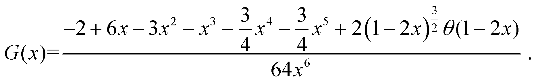
 , where Isat is the intensity of light at which the change of NLR index saturates, λ is the wavelength, α1 is the linear absorption coefficient and the absorption depth can be defined as α1−1. The nonlinear phase shift will be limited if nonlinear losses predominate in materials with potent multiphoton absorption. Then for the MPA, the absorption depth can be described as (I0α2)−1 and (I02α3)−1, where α2 and α3 are the 2PA and 3PA coefficients, respectively. The corresponding figures of merit (FOM) are defined as: