
Performance of the nanopost single-photon source: beyond the single-mode model†
Martin Arentoft
Jacobsen
 a,
Yujing
Wang
a,
Luca
Vannucci
a,
Julien
Claudon
b,
Jean-Michel
Gérard
b and
Niels
Gregersen
*a
a,
Yujing
Wang
a,
Luca
Vannucci
a,
Julien
Claudon
b,
Jean-Michel
Gérard
b and
Niels
Gregersen
*a
aDTU Electro, Department of Electrical and Photonics Engineering, Technical University of Denmark, Ørsteds Plads, Building 343, DK-2800 Kongens Lyngby, Denmark. E-mail: ngre@dtu.dk
bUniv. Grenoble Alpes, CEA, Grenoble INP, IRIG, PHELIQS, “Nanophysique et Semiconducteurs” Group, F-38000 Grenoble, France
First published on 10th February 2023
Abstract
We present a detailed analysis of the physics governing the collection efficiency and the Purcell enhancement of the nanopost single-photon source. We show that a standard single-mode Fabry–Pérot model is insufficient to describe the device performance, which benefits significantly from scattering from the fundamental mode to radiation modes. We show how the scattering mechanism decouples the collection efficiency from the Purcell enhancement, such that maximum collection efficiency is obtained off-resonance. Finally, we discuss how this scattering mechanism can be beneficial for future single-photon source designs.
1. Introduction
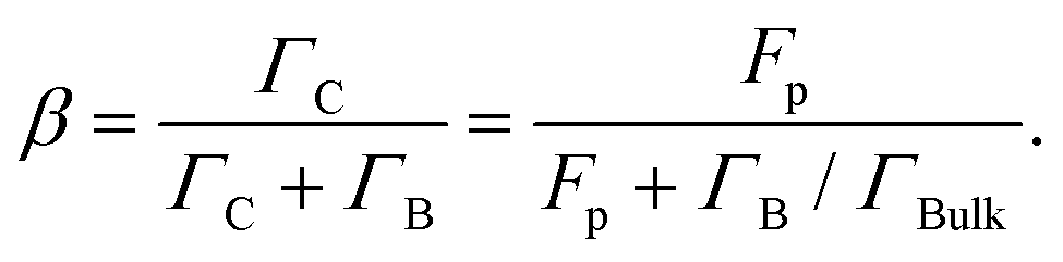
The construction of scalable optical quantum technologies1,2 relies on the development of sources of single indistinguishable photons3–6 and of entangled photon pairs.7 The ideal single-photon source (SPS) should be deterministic and feature pure emission of single photons. The main figure of merit6 is the collection efficiency ε defined as the number of photons detected in the out-coupling channel per trigger. In a multi-photon interference experiment8 with N photons, the success probability P scales as P = εN, and increasing ε towards 1 is thus critical to achieve scalable optical quantum information processing. The spontaneous parametric down conversion process9 is a straight-forward technique widely used within the quantum optics community for production of highly indistinguishable photons, however its probabilistic nature limits the efficiency of pure photon emission to a few percent.For this reason, the community has turned its attention towards two level systems, in particular the semiconductor quantum dot3,4,10 (QD), capable of deterministic emission of single photons. For a QD in a bulk material, ε is limited to a few percent this time due to the large index contrast at the semiconductor-air interface. It is thus necessary to place the QD inside a photonic nanostructure5,6 directing the light towards the collection optics. A main strategy for controlling the light emission is to place the QD inside a micro cavity and exploit cavity quantum electrodynamics (CQED) in the weak coupling regime to selectively enhance the light emission into the optical mode of the microcavity using the Purcell effect.11 Detailed understanding of the CQED physics governing the collection efficiency can be obtained using a single-mode Fabry–Pérot description12–14 of the light emission. Here, the spontaneous emission β factor describes the emission rate ΓC of the QD into a fundamental HE11 cavity mode divided by the total emission rate ΓT = ΓC + ΓB including a contribution ΓB to background radiation modes. The rate ΓC into the cavity mode normalized to the rate ΓBulk in a bulk medium is quantified by the Purcell15 factor 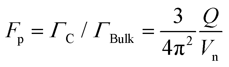 at resonance, where Q is the cavity quality factor and Vn is the mode volume in units of material cubic wavelengths (λ/n)3. The spontaneous emission β factor can then be written in terms of the Purcell factor as
 | (1) |
Furthermore, we define the transmission γ as the fraction of power in the cavity mode detected by the collection optics. Finally, we can then define a single-mode Fabry–Pérot model (SMM) εs for the efficiency as εs = βγ. From eqn (1), we observe that increasing the Purcell factor Fp will improve the collection efficiency, and maximum efficiency is thus expected for a QD on resonance with the cavity.
Indeed, this design paradigm that Purcell enhancement is beneficial for achieving high collection efficiency is well-established within SPS engineering: the most succesful SPS design strategies today include the microcavity pillar14,16–18 and the open cavity approach19 demonstrating up to ε ∼ 0.6 into a first lens16 and into a fiber,19 respectively, combined with highly indistinguishable photon emission. These narrowband approaches, for which the single-mode model εs = βγ is an excellent approximation,14 rely critically on resonant Purcell enhancement and thus on control of the spectral alignment17 to achieve high efficiency. On the other hand, broadband approaches including the photonic nanowire13,20–23 and the photonic crystal waveguide24–26 designs exploit suppression of the background emission rate using the dielectric screening effect20,24,25 to non-resonantly maximize the β factor. Even so, these broadband approaches also benefit from resonant cavity13,27 and slow-light24,25 effects to further improve the efficiency, confirming again that Purcell enhancement is beneficial in the SPS engineering.
However, this paradigm has been challenged by new broadband SPS geometries, such as the circular Bragg grating or “bullseye” design,16,28,29 for which high collection efficiency is obtained in a wavelength range significantly broader28 (∼100 nm) than the typical resonance linewidth (∼10 nm). Similar characteristics were observed very recently for the nanowire optical nanocavity or “nanopost” design30 shown in Fig. 1, for which a significant Purcell factor Fp of 5.6 enabled by the ultrasmall mode volume of the nanocavity was experimentally demonstrated. Additionally, a surprisingly high collection efficiency of 0.35 was measured,30 which was attributed to a breakdown31 of the single-mode model εs = βγ for the efficiency.
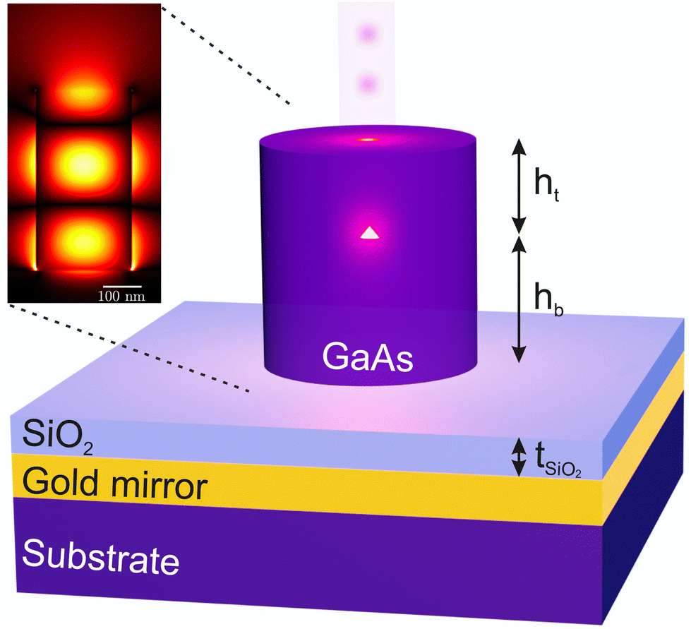 | ||
| Fig. 1 Sketch of the “nanopost” nanowire optical nanocavity and the geometrical parameters. The resulting in-plane electrical field profile of a QD placed inside the nanopost is shown as an inset. The length of the white scale bar in the inset is 100 nm. | ||
In this work, we investigate this surprising breakdown by performing a detailed quantitative analysis of the physics governing the nanopost geometry. We show that the single-mode model fails to describe the physics of both the Purcell enhancement and the collection efficiency due to a decoupling between the two: the computed efficiency is significantly higher than the prediction of the single-mode model thanks to additional transmission channels to the far-field, whose beneficial contributions are dominating over the resonant cavity effect. We show not only that maximum Purcell enhancement and maximum collection efficiency are obtained for entirely different design parameters, but also that maximum efficiency is obtained off-resonance. The analysis is performed using a Fourier modal method,32 allowing for direct insight into the beneficial interplay beyond the single-mode model with the continuum of radiation modes.
This article is organized as follows: in section 2, we present the nanopost and its performance in terms of Fp and ε, and we demonstrate the breakdown of the single-mode model. In section 3, we present our theoretical framework based on the Fourier modal method, which we subsequently use to analyze the complex interplay with radiation mode channels in section 4 and its influence on the collection efficiency and the Purcell factor. In section 5 we put the nanopost physics into perspective and discuss its impact on SPS engineering, followed by our conclusion. Additional simulation results are presented in the ESI.†
2. The nanopost geometry and the breakdown of the single-mode Fabry–Pérot model
The nanopost shown in Fig. 1 consists of a truncated GaAs nanowire with diameter D on top of a SiO2-Au mirror. The top of the nanowire is flat, and the surrounding medium is air. The SiO2 layer, located between the nanowire and the gold, has a thickness indicated by tSiO2. We note that the main difference between the nanopost and the photonic nanowire13,20–23 geometries is the flat top of the nanopost resulting in substantial reflection, thus creating a cavity. On the other hand, the photonic “needle” structure,21 as well as the “trumpet” structure23 featuring a top anti-reflection coating, are half-open 1D photonic structures. The QD, modelled as a dipole, is placed on-axis inside the nanowire at a position hb from the bottom interface and ht from the top interface. The refractive indices of the materials are chosen as nGaAs = 3.46, nSiO2 = 1.5 and nAu = 0.201 + 5.85i at λ = 930 nm and assumed to be constant as a function of wavelength. In the inset of Fig. 1, a dipole with an emission wavelength of 930 nm is placed inside the nanopost, and the resulting in-plane electrical field, simulated using the FMM, is shown. Three antinodes can be seen in the field profile, corresponding to the order 3 cavity mode, and they are enumerated from the bottom mirror as the 1st, 2nd and 3rd antinode. The field profile generated by the dipole is independent of the vertical position of the dipole, only the intensity changes. The intensity is not the same at the three antinodes due to the breakdown of the SMM.We now present the performance of the nanopost as a function of the diameter, D, and the silica layer thickness, tSiO2. We have scanned the parameter ranges D = 196 nm to D = 300 nm and tSiO2 = 0 nm to tSiO2 = 25 nm and chosen a design wavelength of λd = 930 nm. The height of the structure and the position of the QD are dynamically changed to keep the order 3 cavity mode resonance at λr = 930 nm for the QD at the 2nd antinode. The required procedure is presented in ESI section 1.†
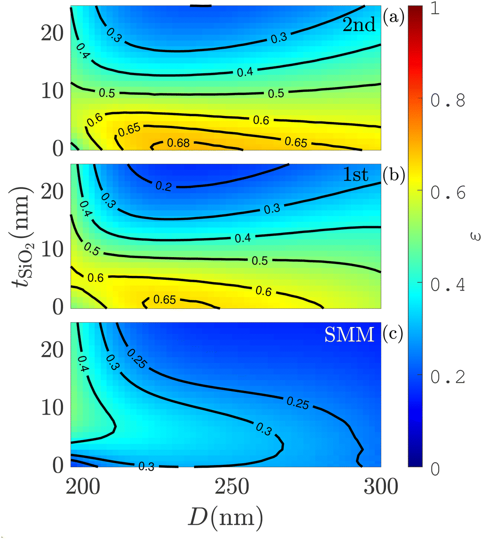
The first quantity of interest is the spontaneous emission rate ΓT. For the high-β structures investigated here, the total normalized rate ΓT/ΓBulk and the Purcell factor Fp are similar, and we will in the following refer to the normalized total rate as the “Purcell factor Fp”. In Fig. 2a and b the Purcell factor is shown as a function of the diameter and the silica layer thickness for a QD placed in the 2nd and 1st antinode. In the entire parameter space, the Purcell factor is larger for the 2nd antinode and a maximum value of Fp = 7.9 is reached at D = 25 nm and tSiO2 = 13 nm. This discrepancy between the two antinodes also demonstrates the deviations of the SMM. Overall, the tendency of the Purcell factor is similar at the 2 antinodes with one peak value. The minimum is located in the corner of no silica and the smallest diameter. In Fig. 2c the Purcell factor is now shown using the SMM. Comparing the SMM to the full model for the two antinodes, there are both positive and negative deviations across most of the parameter space. Compared to the 2nd antinode, the SMM also predicts a slightly lower value for the maximum Purcell factor of Fp = 7.5, but at a very different position of D = 242 nm and tSiO2 = 8 nm. However, compared to the 1st antinode the SMM predicts a larger value for the maximum Purcell factor. This is an invitation to obtain a better description and understanding of the physics responsible for the Purcell factor, which we will provide in this paper.
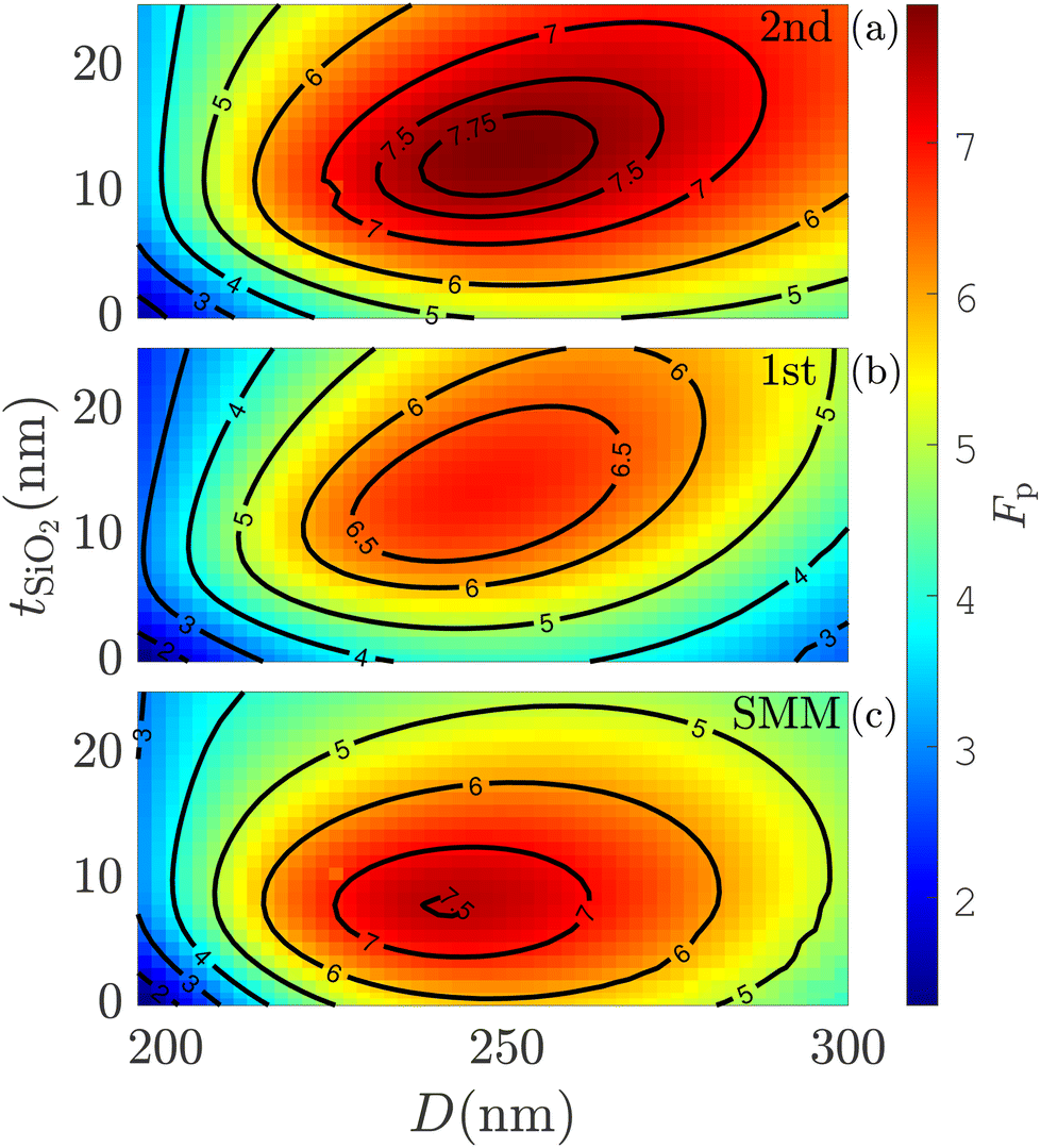 | ||
| Fig. 2 Purcell factor, Fp, for a QD at the 2nd antinode (a), 1st antinode (b) and any antinode using the SMM (c) as a function of the diameter, D, and the silica layer thickness, tSiO2. | ||
The source collection efficiency, ε, for the 2nd antinode, the 1st antinode and the SMM are shown in Fig. 3 for a numerical aperture of NA = 0.75. Here the overall performance for the 2nd antinode is slightly better than for the 1st antinode, and a maximum value of ε = 0.69 is reached at D = 238 nm and tSiO2 = 0 nm. Despite the very simple geometry of the nanopost, a surprisingly high collection efficiency of ε = 0.69 is achievable. In general, it can be ascertained that no silica layer is more beneficial for the efficiency, which is surprising compared to the traditional photonic nanowire, where the silica layer enhances the modal reflectivity21 and thus the collection efficiency. Now comparing the efficiency of the SMM to the full model, there are substantial differences. This is unlike the micropillar and the photonic nanowire geometries for which the single-mode model εs = βγ is an excellent12–14 approximation. For the nanopost, the SMM efficiency is much smaller in the entire parameter space except for the smallest diameters. This clearly shows that there are important physical mechanisms which are not accounted for in the SMM. Furthermore, comparing the figures for the Purcell factors and the efficiencies, there seems to be no apparent correlation between the two. This is also a surprising result compared to traditional Fabry–Pérot cavities and indicates that there are different physical mechanisms at play which govern the Purcell factor and the efficiency.
 | ||
| Fig. 3 Collection efficiency, ε (NA = 0.75), for a QD at the 2nd antinode (a), 1st antinode (b) and any antinode using the SMM (c) as a function of the diameter, D, and the silica layer thickness, tSiO2. | ||
In ESI section 2,† we vary the numerical aperture and present its influence on the collection efficiency. In ESI section 3,† we present the collection efficiency taking into consideration the overlap with a Gaussian profile.
3. Theory
3.1. Method
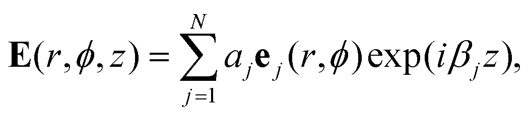
We use an eigenmode method combined with a standard scattering matrix formalism33 in the frequency domain. In this method, the structure is divided into layers of uniform permittivity along the propagation direction. In each layer, the electrical field is expanded on the eigenmodes, and the scattering matrices are used to connect the eigenmodes at the interfaces between the layers. The eigenmodes are obtained using the Fourier modal method (FMM) with open boundary conditions,32 which provides direct access to the modes needed to understand the physics. The nanopost structure is split into four layers: the bottom gold substrate, the silica layer, the nanowire and the top air region. Due to the cylindrical symmetry of the nanowire, a cylindrical coordinate system is used. The QD is modelled as a classical point dipole, and we make use of the relationship Γ/ΓBulk = P/PBulk to calculate the Purcell factor.34P is the emitted power of the dipole, and PBulk is the power emitted in a bulk medium, and thus the Purcell factor is defined as FP = PT/PBulk. The second quantity of interest is the collection efficiency defined as ε = Pcollected/PT, where Pcollected is the power collected in the far-field of a lens with numerical aperture NA.| Ej(r,ϕ,z) = ej(r,ϕ)exp(iβjz), | (2) |
 , where nlayer is the refractive index, k0 is the free-space wavenumber and k⊥ is the in-plane k-value. k⊥ can take any value k⊥∈[0,∞] and eigenmodes exist for all the values. For each β, two orthogonal solutions exist, which can be separated into TE modes (ez = 0) and TM modes (hz = 0). For layers with real-valued refractive index, this continuum can be separated into radiation modes satisfying 0 < (β)2 ≤ (nlayerk0)2 and evanescent modes (β)2 < 0 which decays exponentially and carry no power according to the Poynting vector. Specifically for the air layer, the propagation constant of the radiation modes can directly be interpreted as the propagation angle with respect to the z-axis using the expression θ = arccos (β/k0). Expanding a forward propagating electrical field on the eigenmodes will have the following expression:
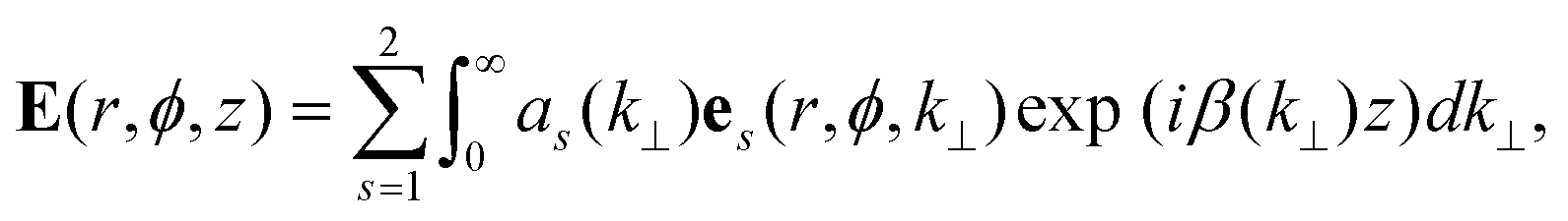 | (3) |
 | (4) |
The first class of eigenmodes for the nanowire are the guided modes for which the propagation constants satisfy the condition (nairk0)2 < (βj)2 < (nGaAsk0)2. The guided mode is confined to the core of the nanowire, and outside the nanowire, the field decays. There is a finite number of guided modes, and there will always be at least one guided mode, the fundamental HE11 mode. The description of guided modes can be found in various textbooks.36 The second class of eigenmodes is the background continuum, very similar to the continuum of the air layer. These eigenmodes can be viewed as perturbed versions of the cylindrical plane waves of the air layer and be separated into radiation and evanescent modes the exact same way. There are also two orthogonal solutions, but these can no longer be separated into pure TE and TM modes. Studies of this class of eigenmodes are plentiful in the literature.37–46
 | (5) |
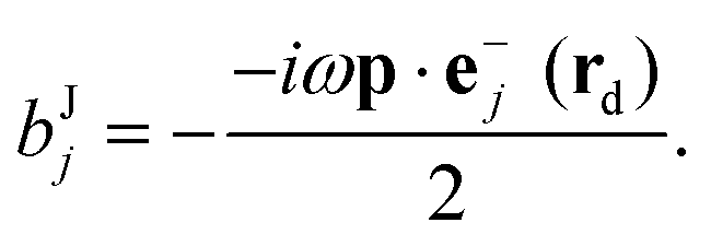
The total emitted power, PT, can be calculated by evaluating the total field, ET(rd), but also the power into individual modes, Pj, by evaluating Ej(rd). Placing the dipole on-axis inside an infinitely long nanowire with position zJ will result in the following electrical field:
 | (6) |
 | (7) |
 | (8) |
 | (9) |
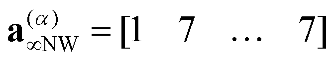
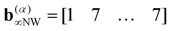
The expansion coefficients can then be represented by vectors:
 | (10) |
 | (11) |
 | (12) |
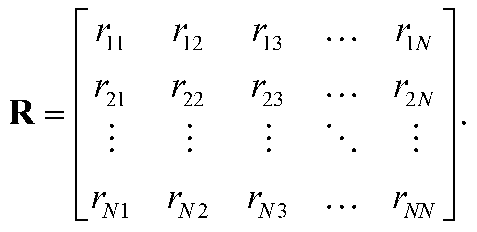
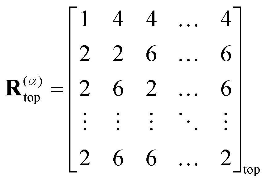
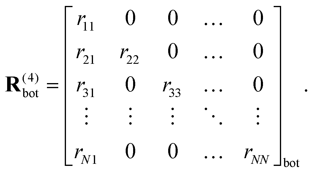
The r11 coefficient represents the reflection of the fundamental mode back into itself, while the remaining part of the first column represents the reflection of the fundamental mode into all other modes and so forth. Propagation matrices are used to propagate the field inside a layer and are defined in the following way:
 | (13) |
The total field inside the structure can then be calculated by taking into account the round-trips which the initially emitted light takes inside the cavity. Above the emitter, the field takes the following expression:33
 | (14) |
where the new expansion coefficients are calculated using the following equation:33
 | (15) |
| btot = P(ht)RtopP(ht)aJtot. | (16) |
Now the Purcell factor can be calculated by evaluating the total field at the dipole position using eqn (5).
| aair = TtopP(ht)aJtot. | (17) |
To calculate the collected power in a lens with some numerical aperture, a near- to far-field transformation is used.47 The far-fields EFF(R,θ,ϕ) and HFF(R,θ,ϕ) are calculated on the surface of a sphere with radius R, and the radial component of the resulting Poynting vector is:
 | (18) |
The collected power in the far-field is then:
 | (19) |
 | (20) |
| btot,SMM = aJtot,SMMr11,topei2htβ1. | (21) |
The collected power in the far-field is then calculated by inserting eqn (20) into eqn (17), and the SMM efficiency is then defined as εs = Pcollected,SMM/PT, equivalent to the definition in the introduction.
3.2. Mode-coupling and emission channels
Important coupling effects take place at the top and bottom interfaces of the nanowire. At both interfaces, all the modes couple to each other, i.e. all the elements in the reflection matrices are non-zero; however, some modes and elements are more important than others. In Fig. 4, different examples of mode coupling are shown along with the emission channels that will contribute to the far-field. The sketch is divided into two parts: the main channels and the background channels. The main channels consist of all the light that originated as the fundamental mode, αt and αb, which is indicated by the red arrowheads. This is the propagating mode that experiences sufficiently large reflections at both interfaces such that it is Purcell enhanced.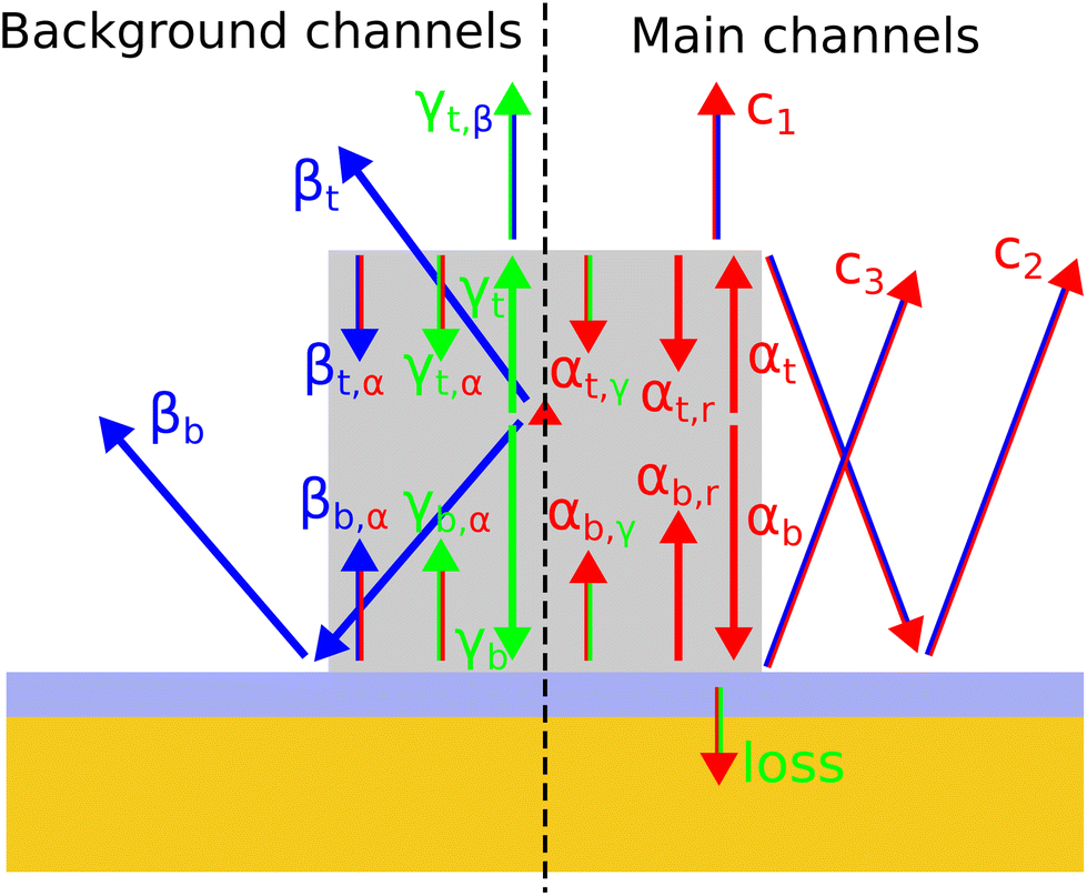 | ||
| Fig. 4 Sketch of the nanopost and the different emission channels and examples of mode-coupling. The emission channels are separated into the main channels and the background channels. The red color corresponds to the fundamental mode, the blue color corresponds to radiation modes and the green color corresponds to evanescent modes. Some arrows have two colors, where the color of the arrowhead corresponds to the original channel, but the 2nd color on the shaft signifies the current mode classification. As an example consider c1 which is the transmission of the fundamental mode into the air. It has a partly blue shaft as it is now classified as radiation, but it originated as the fundamental mode (red arrowhead). See main text for more information. | ||
• Transmitted into the air indicated by c1.
• Reflected, indicated by αt,r (the channel responsible for Purcell enhancement).
• Scattered into radiation that propagates downwards indicated by the red/blue arrow pointing towards the bottom mirror. This radiation will then be reflected by the bottom mirror and then be transmitted into the air indicated by c2.
• Coupled to evanescent modes indicated by αt,r.
At the bottom interface the fundamental mode is:
• Transmitted into the mirror and lost indicated by the green/red arrow pointing downwards at the very bottom.
• Reflected, indicated by αb,r (the channel responsible for Purcell enhancement).
• Scattered into radiation that propagates towards the air indicated by c3.
• Coupled to evanescent modes indicated by αb,γ.
As we will demonstrate in the following, the three radiation channels c1, c2 and c3 are the main channels that will contribute to the far-field.
4. Analysis of the Purcell factor and efficiency
The starting point of the analysis is the emission rates in the infinitely long GaAs nanowire, which directly represent the initial coefficients of eqn (10) and (11) through eqn (5) and (7). In Fig. 5, the emission rates for the present guided modes, the radiation modes and the total emission are shown as a function of the nanowire diameter. The black dotted vertical lines represent the interval which is used in the full simulations of the nanopost. In this interval, the infinite nanowire only contains one guided mode, the fundamental HE11 mode, and most of the power is emitted into this mode. The emission into radiation is suppressed in most of the interval and only begins to increase when the diameter reaches 300 nm before the EH11 mode appears. The emission rates thus show that the radiation background channel (the initial coefficients for the radiation) presumably only has a minor influence on the Purcell factor and efficiency as long as the cavity does not suppress the fundamental mode. Fig. 5 cannot be used to quantify the importance of the evanescent background channels, as the field components of the evanescent eigenmodes only have a real part. Later on, in the third subsection, models will be used to quantify the effect of the evanescent background channels the finite-length nanopost structure.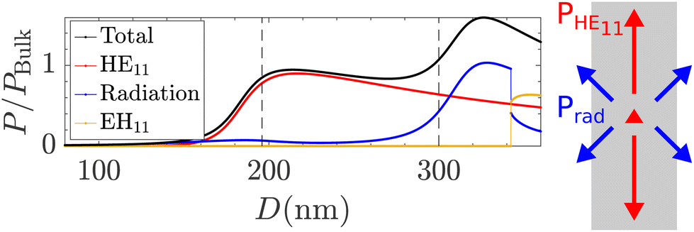 | ||
| Fig. 5 Power emission in the infinite nanowire as a function of the diameter, D. A sketch of the emission in an infinite nanowire with an embedded QD is shown in the right part of the figure. | ||
4.1. Scattering of the fundamental mode at the interfaces
Here, we will study reflection and transmission at the top interface between the GaAs nanowire and the air above. The fundamental mode is launched towards the interface, and then the reflection and transmission coefficients are calculated. The power reflection coefficient for reflection of mode n into mode m is Rm,n = |rm,n|2, and the power transmission coefficients are defined similarly. The total power reflection of the fundamental into radiation is then defined as , and in the discretized regime
  , where the index Nk0,wire corresponds to the total number of radiation modes in the nanowire. Thus the total power reflection of the fundamental mode is Rtotal,1 = R1,1 + Rrad,1. The total power transmission of the fundamental mode is then defined as
  and due to power conservation we have Rtotal,1 + Ttotal,1 = 1.
In Fig. 6, the power reflections, along with the power transmission of the fundamental mode, are shown as a function of the nanowire diameter D. By comparing the magnitudes of the modal reflection (R1,1) and the reflection into radiation (Rrad,1), it is clear that the reflection into radiation (c2 in Fig. 4) is essential for the far-field. This indicates why the SMM fails to describe the efficiency. This mechanism will have a much smaller influence on the Purcell factor as the radiation modes only has a small field amplitude at the center of the nanowire shown in the previous section (Fig. 5). However, the reflection matrix is approximately symmetric, such that the first column and the first row is identical, r1,n ≈ rn,1. This means that a small part of the radiation will actually scatter back into the fundamental mode at the top interface, and this will have an influence on the Purcell factor, which we will show later. In general for Fig. 6, we observe small modal reflections for small diameters and this will lead to a limited cavity effect and thus a lower Purcell factor.
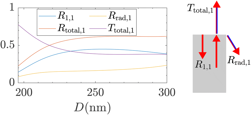 | ||
| Fig. 6 Reflection and transmission of the fundamental mode as a function of the diameter, D, at the top interface. A sketch of top interface and the reflection and transmission of the fundamental mode is seen to the right. | ||
We now consider the reflections at the bottom interface between the GaAs nanowire and the silica-gold mirror. Compared to the top interface, there is now an additional parameter, namely the thickness of the silica layer, tSiO2. The purpose of the silica layer is to increase the reflection of the fundamental mode and avoid coupling to surface plasmons which would decrease the reflection.48 In Fig. 7, the bottom reflection coefficients are shown as a function of the diameter and the silica layer thickness. In the parameter ranges where the modal reflection is large ∼0.9 (strong cavity effect), the reflection into radiation is small ∼0.01. Here we do not expect a significant contribution of the scattering into radiation, c3. However, as the modal reflection decreases, the reflection into radiation increases to larger values ∼0.1, and here c3 will contribute to the far-field. For small diameters and low values of the silica layer thickness, the modal reflection is small (weak cavity effect) and the scattering into radiation is very large ∼0.2. This behavior has been described in the literature.48
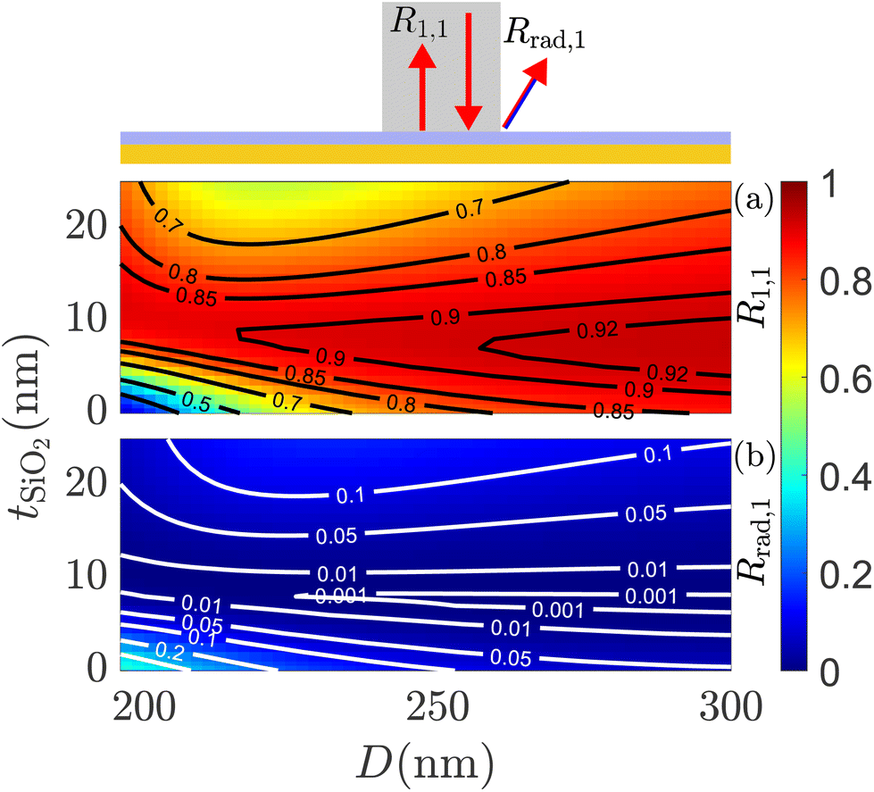 | ||
| Fig. 7 (a) Modal reflection, R1,1 and (b) reflection into radiation of the fundamental mode, Rrad,1, as a function of the diameter, D, and silica layer thickness, tSiO2, at the bottom interface. A sketch of the bottom interface is shown in the top part of the figure. | ||
Due to the scale invariance of Maxwell's equations, both the top and bottom reflections are broadband, which gives the potential for broadband Purcell enhancement.
4.2. Enhanced efficiency
In the first part of this subsection, we present different methods to model the efficiency to show how important the different emission channels are. Then we will apply the modelling methods on the structure with the largest efficiency, namely D = 238 nm and tSiO2 = 0 nm with a QD placed at the 2nd antinode.In the first method, the reflection and transmission matrices are unchanged; however, a varying number of the initial coefficients, a∞NW and b∞NW of eqn (10) and (11), are included when aJtot (eqn (15)) and thus Pcollected is calculated. For instance, if we only include the first element of the initial coefficients, aJ1 and bJ1, and put the remaining elements to zero, then we only include the main channels in Pcollected, which originated as the fundamental mode. As we increase the number of initial coefficients included, the background channels are added starting from the first radiation mode until the last evanescent mode. ε can then be plotted as a function of the included initial coefficients and if this curve is flat, then the main channels dominate the efficiency.
In the second method, the reflection and transmission matrices are also unchanged, all initial coefficients are included, but instead, a varying number of the final coefficients, aJtot of eqn (15), are included when Pcollected is calculated. The first element of aJtot represents all the light that ended up in the fundamental mode, where the main contribution is from the fundamental mode itself, but also includes contributions of the background channels which have scattered into the fundamental mode such as βt,α, βb,α, γt,α and γb,α seen in Fig. 4. However, by using the first method, we can quantify how strong these contributions are. If these contributions are weak, then the main channels are dominating. Thus if only the first element of the final coefficients is included in Pcollected, then only the direct transmission of the fundamental mode is included in the far-field, namely c1 in Fig. 4. Then as we increase the number of elements of the final coefficients, the contributions of c2 and c3 are included. In principle, channels such as βt and βb are also included, but again we use the previous method to quantify these. ε can then be plotted as a function of the included final coefficients, and if this curve is increasing, then the channels c2 and c3 are contributing to the efficiency.
Finally, we wish to visualize the interference between the direct transmission of the fundamental mode and the scattered channels by calculating the transmission of the fundamental mode and the entire background continuum separately:
| aair,HE11 = TtopP(ht)aJtot,HE11 | (22) |
| aair,BG = TtopP(ht)aJtot,BG, | (23) |
 | (24) |
 | (25) |
Then the phase difference between the two contributions can be calculated:
| Δϕ = arg(aair,HE11) − arg(aair,BG). | (26) |
The phase difference will be separated into TE and TM modes. Along with the phase difference, the far-field plots of the direct transmission of the fundamental mode (aair,HE11), the entire background continuum (aair,BG) and the total field (aair) will be shown.
 | ||
| Fig. 8 (a) Efficiency, ε (NA = 0.75), as a function of the initial coefficients expressed with the propagation constant (β/k0)2. (b) Efficiency, ε (NA = 75), as a function of the final coefficients expressed with the propagation constant (β/k0)2. | ||
Now we will visualize the interference between the direct transmission of the fundamental mode and the scattered channels by inspecting the phase changes and the far-fields. In Fig. 9a, the phase difference in the air layer between the direct transmission of the fundamental mode and the entire background is shown as a function of the propagation constant for TE and TM modes. For the light that propagates vertically, the phase difference is close to zero, such that there is constructive interference between the direct transmission and the background radiation. For the light that propagates horizontally, the phase difference is closer to π, and thus there is destructive interference. In Fig. 9b, c and d the far-fields of the direct transmission of the fundamental mode, the background radiation and the total field are shown. Here we can directly observe the effect caused by the phase difference. In the center of the total far-field, the field is enhanced due to the constructive interference, but for the light that propagates horizontally there is destructive interference. As such, the interference between the direct emission and the radiation focuses the far-field.
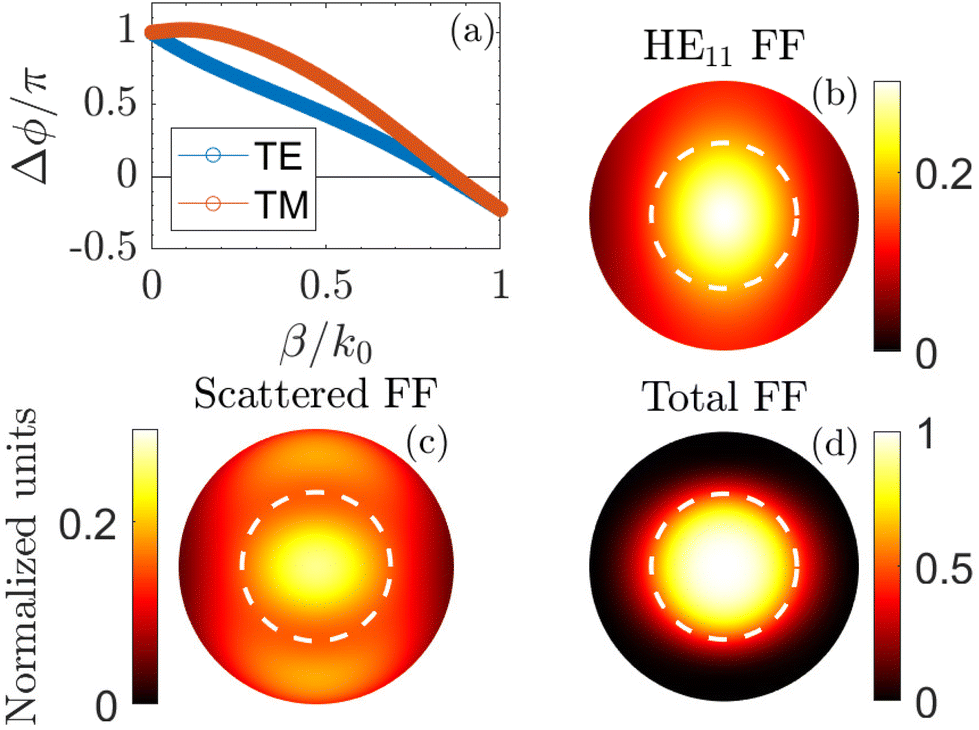 | ||
| Fig. 9 (a) The phase difference between the direct transmission of the fundamental mode and the background continuum for TE and TM modes as a function of the propagation constant, β/k0. (b) The far-field of the fundamental mode. (c) The far-field of the background continuum. (d) The total far-field. The white dotted line indicates NA = 0.75. Be aware of the different color scales that have been used for the far-fields. | ||
A similar analysis of the efficiency for the structure with the largest Purcell factor is included in ESI section 4.†
4.3. Enhanced Purcell factor
As shown in Fig. 2, there are deviations between the full model and the SMM for the Purcell factor, and we wish to understand where these deviations appear. Therefore we will introduce a model which can identify where these deviations appear and apply the model on the structure with the largest Purcell factor, namely D = 250 nm and tSiO2 = 13 nm.1. SMM
2. Scattering of the fundamental mode at the top interface
3. Scattering of the fundamental mode at the bottom interface
4. Back-scattering of the background continuum to the fundamental mode at the top interface
5. Back-scattering of the background continuum to the fundamental mode at the bottom interface
6. Scattering of the background continuum to itself at both interfaces
7. Including initial background continuum
Steps number 4 and 5 correspond to the process HE11 → radiation/evanescent → HE11 which is a recycling effect, and we will show the importance of this process for the Purcell factor. Step number 6 corresponds to the process radiation/evanescent → radiation/evanescent, which also opens up for further scattering channels such as radiation/evanescent → radiation/evanescent → HE11.
The 7 steps can then be translated to the initial inputs and the top and bottom reflections in the following schematic way:
 | (27) |
 | (28) |
 | (29) |
 | (30) |
Here, the superscript α represents the seven complexity steps. For a given step α, each matrix entry >α is set to zero, while entries ≤α keep their original value. We will use the step α = 4 as an example:
 | (31) |
 | (32) |
 | (33) |
 | (34) |
At each step in the previous model building, the entire background continuum was added, i.e. the entire column or row was added at once. As such, it is difficult to quantify which part of the background continuum that is important. Therefore we will also present the models where the elements for the background continuum are increased one at a time. In this way it can be quantified how the different parts of the background continuum contribute to the Purcell factor.
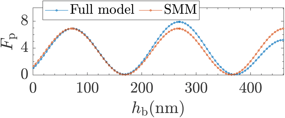 | ||
| Fig. 10 Purcell factor, Fp, computed using the full model and SMM as a function of the dipole position from the bottom interface, hb. D = 250 nm and tSiO2 = 13 nm. | ||
In Fig. 11a and b, the Purcell factor and the power enhancement of the fundamental mode are shown as a function of the model complexity progression for the 1st and 2nd antinode (model complexity number α will be shortened n. α). Evidently, the analysis of the Purcell factor is complicated due to contributions of the entire background continuum, multiple scattering channels and feedback mechanism. Therefore there are changes in the Purcell factor for all steps in the model complexity, which makes it challenging to model the Purcell factor using only a few modes. The continuum of radiation modes can be modelled using leaky modes, which can enable the modelling using only a few modes. This has been demonstrated in photonic crystal microcavities where strong feedback mechanisms also were present.49 However, by using the presented model, we will obtain an in-depth physical insight.
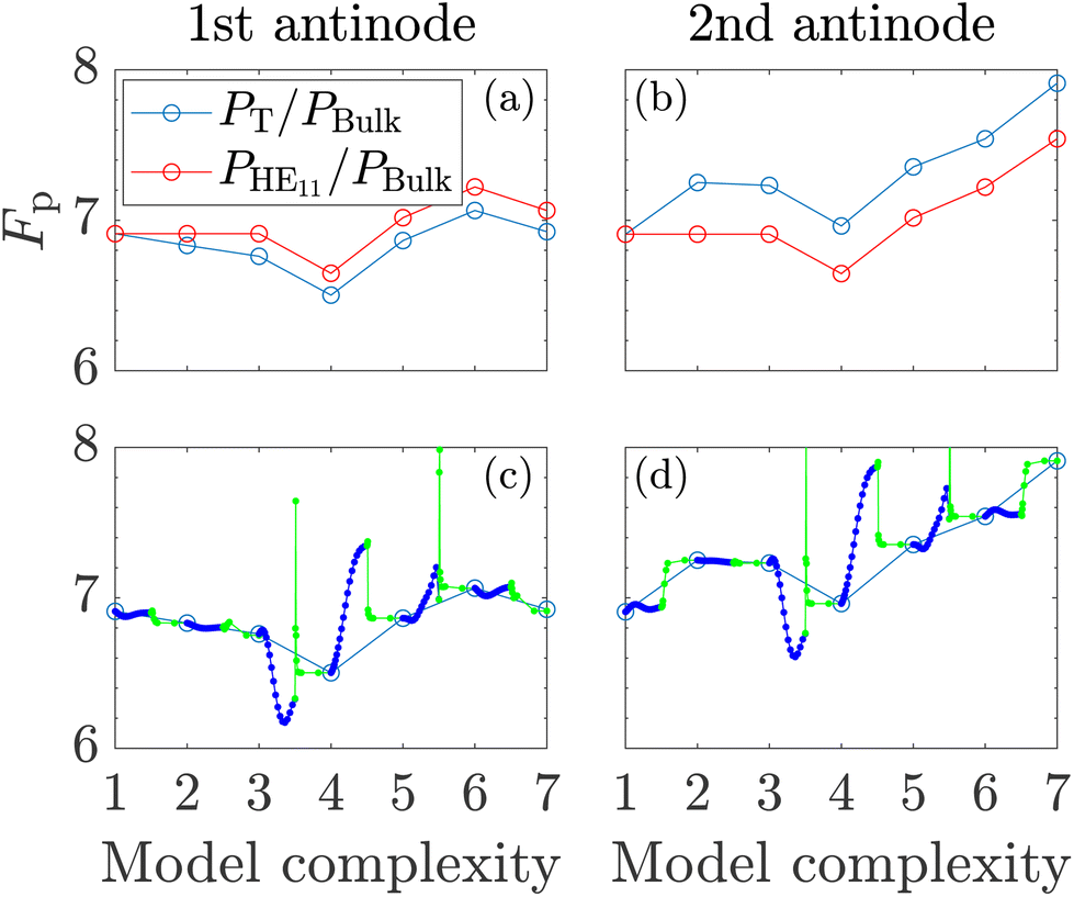 | ||
| Fig. 11 Purcell factor (PT/PBulk) and fundamental mode enhancement (PHE11/PBulk) for the 1st (a) and 2nd (b) antinode as a function of the model complexity progression. In (c) and (d) the background continuum is continuously included between each model complexity. | ||
The Purcell factor starts at the same value with the SMM for both antinodes. By including scattering of the fundamental mode at the top interface (n. 2) there is a significant increase for the 2nd antinode but a very small decrease for the 1st antinode. Already now, the deviations compared to the SMM have started to appear. By including the scattering at the bottom interface (n. 3) the 2nd antinode is almost unaffected, but a small decrease appears for the 1st antinode. Now including the back-scatteringat the top interface (n. 4), there is a large decrease in the Purcell factor at both antinodes. This decrease is directly represented in PHE11/PBulk. Interestingly, when including the back-scattering at the bottom interface (n. 5), there is now a large increase in the Purcell factor at both antinodes, which is also represented in PHE11/PBulk. This also shows that the recycling effect HE11 → radiation/evanescent → HE11 can provide both negative and positive contributions. When the background is allowed to scatter to itself, i.e. radiation/evanescent → radiation/evanescent (n. 6), there is an increase for both antinodes. This increase is directly represented in PHE11/PBulk, which in fact means that the process radiation/evanescent → radiation/evanescent → HE11 is dominating compared to radiation/evanescent → radiation/evanescent itself. Finally, by including the initial background (n. 7), there is an increase for the 2nd antinode but a decrease for the 1st antinode. These changes also correspond to the change in PHE11/PBulk, which means it is the process of radiation/evanescent → HE11 that is important for the initial background.
The main differences between the two antinodes appear, when the fundamental mode scatters at the top interface (n. 2) and when the initial background (n. 7) is included. To better understand which part of the background continuum is important, we will also consider the continuous steps of the model complexity. This is now shown in Fig. 11c and d. Here we observe that the main positive contributions at the 2nd antinode are due to the slowly decaying evanescent modes. This is the process of HE11 → evanescent at the top interface and the process of the initial background evanescent → HE11. For the back-scattering at the interfaces (n. 4 and n. 5), we observe that the propagating radiation modes can also significantly affect the Purcell factor.
An additional important observation is that PHE11/PBulk exceeds PT/PBulk for the first antinode due to the negative contributions. This would in fact result in β factors above 1 using the definition βHE11 = PHE11/PT. This indicates that the β factor might not be a suitable figure of merit for structures where the SMM breaks down, or at least one should be very careful in the definition of the β factor. Alternatively, the typical interpretation of the β factor as a standard power fraction should be reconsidered in the regime of the SMM breakdown.
The analysis of the Purcell factor for the structure with the largest efficiency, D = 238 nm and tSiO2 = 0 nm, is included in ESI section 5.†
4.4. Wavelength dependence
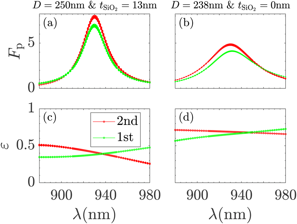
In this section, we will present the broadband performance of the nanopost. The focus will be on the designs with the largest Purcell factor and efficiency, respectively.In Fig. 12a, the Purcell factor is shown as a function of the wavelength for the 1st and 2nd antinode of the structure with the largest Purcell factor. The Purcell factor of the 2nd antinode performs better than the 1st antinode close to the resonance wavelength, and the spectral width at FWHM (full width half maximum) of the antinodes are approximately Δλ2nd = 27 nm and Δλ1st = 28 nm showcasing the broadband performance. The spectrum for the two antinodes is not completely symmetric, and the two curves for the antinodes also cross further away from the resonance. In Fig. 12b, the Purcell factor is shown as a function of the wavelength for the 1st and 2nd antinode of the structure with the largest efficiency (at resonance). Here the Purcell factor is much lower and the spectral width much broader at Δλ2nd = 52 nm and Δλ1st = 56 nm. Furthermore, the resonance wavelength for the 1st antinode is slightly shifted to λr = 931.5 nm. This can be explained by the low Q factor and the neighbouring low Q factor cavity modes, i.e. the cavity modes with 2 and 4 antinodes. Due to the low Q factor, there is a small spectral overlap causing the slight shift. In the ESI section 6,† we present a nanopost design where the resonance wavelength shift is more pronounced between the two antinodes.
 | ||
| Fig. 12 (a) and (b) Purcell factor, Fp, of the two antinodes for the two structures as a function of wavelength, λ. (c) and (d) efficiency, ε (NA = 0.75), of the two antinodes for the two structures as a function of wavelength, λ. The numerical uncertainty is represented by the thickness of the curves. | ||
In Fig. 12c and d the efficiencies (NA = 0.75) are shown as a function of the wavelength for the 1st and 2nd antinode for the two structures. The main characteristic of the efficiency is that it does not follow the Purcell factor, which is surprising compared to traditional Fabry–Pérot cavities. Instead, the efficiency changes roughly linearly across the resonance, and in general, the slope for the 2nd antinode is negative and positive for the 1st antinode. This means that the maximum efficiency is in fact achieved off-resonance, ε2nd,NA = 0.75(λ = 880 nm) = 0.71, but at a much smaller Purcell factor.
In Fig. 13, βHE11 is shown as a function of the wavelength for the 2nd and 1st antinode and the infinite nanowire. βHE11 is close to 1 (both above and below) in the entire interval, which indicates that the fundamental mode is still the dominating contribution. Due to the broadband βHE11 of the infinite nanowire, it is not required to be on resonance to obtain large values of βHE11, and the QD would need to be very close to a node before βHE11 would decrease. Regardless, the fundamental mode scatters into radiation which affects PT such that βHE11 does not follow a Lorentzian curve like the Purcell factor.
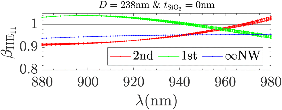 | ||
| Fig. 13 β HE11 = PHE11/PT as a function of the wavelength, λ, for the 2nd and 1st antinode and the infinite nanowire. The numerical uncertainty is represented by the thickness of the curves. | ||
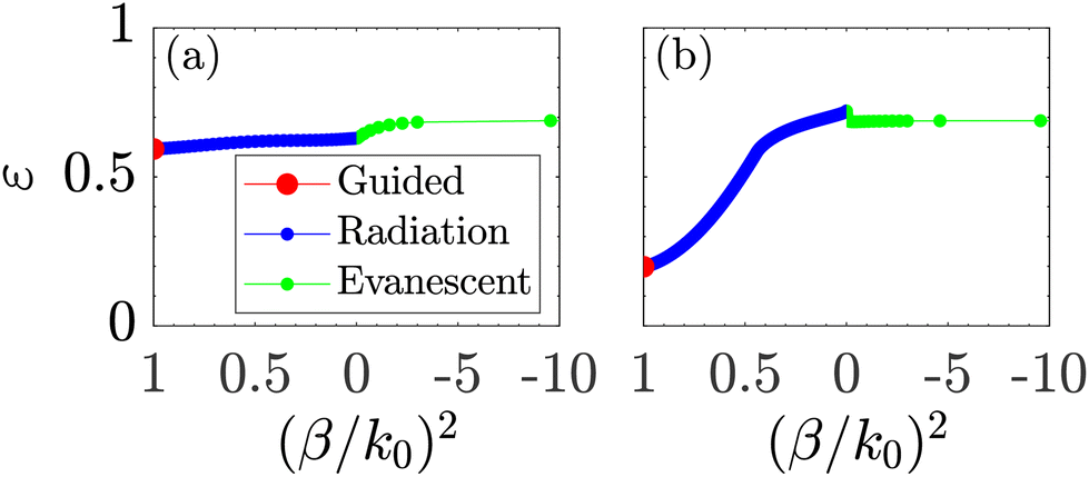
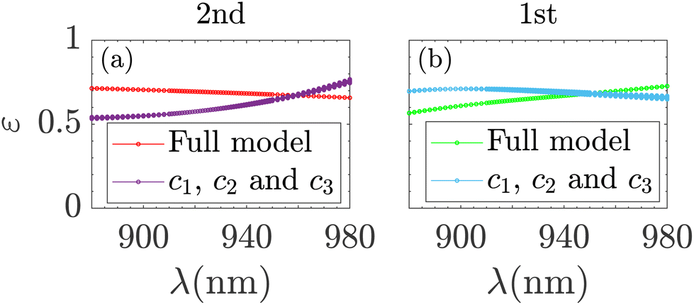
To quantify how dominating the fundamental mode is for the efficiency, we will use the first method presented in section 1 to separate the main channels (c1, c2 and c3) from the background channels. In Fig. 14, we compare the efficiency of the full model to only including c1, c2 and c3 for both antinodes. By comparing to Fig. 13 we observe that the curves for the main channels directly follow the trend of βHE11. However, there is a discrepancy between the efficiency of the full model and only using the main channels of c1, c2 and c3. This discrepancy is not at a minimum on resonance (λ = 930 nm), but almost at the minimum when βHE11 = 1 for both antinodes. We observe that for βHE11 < 1, the background channels provide a positive contribution to the efficiency, while for βHE11 > 1 the background channels provide a negative contribution. This shows that the β factor is still useful in the analysis but not necessarily a figure of merit for SPSs in the breakdown of the SMM. Furthermore, Fig. 14 shows that the background channels still interfere with the main channels causing this discrepancy and even changing the slope of the curves for the efficiency. As an example we will consider two wavelengths for the 2nd antinode and use the first method presented in section 1:
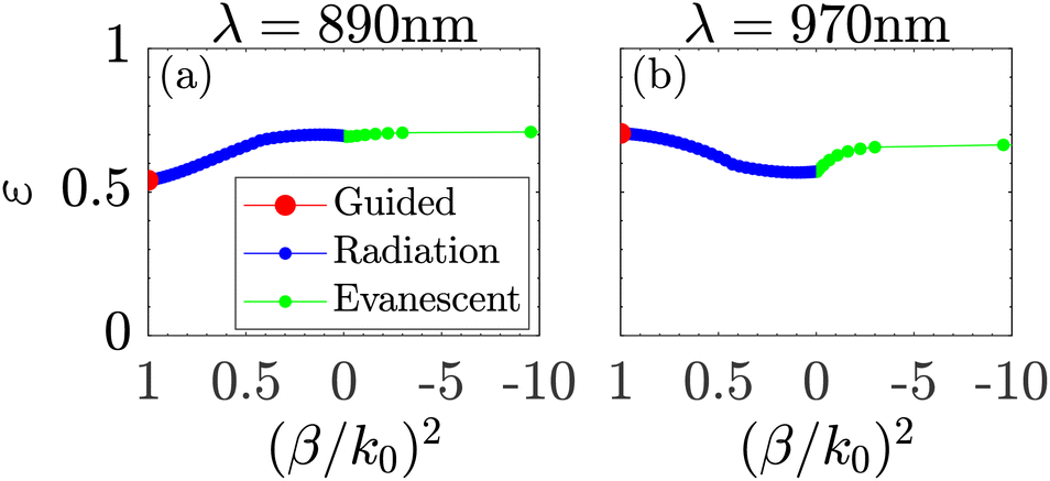
In Fig. 15 the efficiency is shown as a function of the initial coefficients expressed with the propagation constant (β/k0)2 for the two wavelengths λ = 890 nm and λ = 970 nm at the 2nd antinode. Again the first red point corresponds to including all the main channels, and then background channels are added. For λ = 890 nm, the initial propagating background radiation provides a significant increase to the efficiency, while the evanescent modes provide no change. On the other hand, for λ = 970 nm, the initial propagating background radiation provides a significant decrease to the efficiency, while the evanescent modes provide a positive increase to the efficiency. This also showcases the complex interplay between the main channels and the background channels.
 | ||
| Fig. 14 Efficiency, ε (NA = 0.75), as a function of the wavelength, λ, for the 2nd antinode (a) and 1st antinode (b). The full model is compared to only using c1, c2 and c3. D = 238 nm and tSiO2 = 0 nm. The thickness of the curves represents the numerical uncertainty. | ||
 | ||
| Fig. 15 Efficiency, ε (NA = 0.75), as a function of the initial coefficients expressed with the propagation constant (β/k0)2 for λ = 890 nm (a) and λ = 970 nm (b) at the 2nd antinode. | ||
5. Perspective
We have shown that contributions from multiple scattering channels influence both the Purcell factor and especially the collection efficiency. Unlike traditional Fabry–Pérot cavities, where scattering of the light is viewed simply as a loss mechanism, this scattering is in fact beneficial for the performance of the nanopost SPS. Importantly, this scattering mechanism decouples the efficiency from the Purcell factor directly challenging a well-known design paradigm that maximum collection efficiency is obtained on resonance. The identification of this mechanism opens a door to unconventional SPS design approaches, especially in the non-resonant regime where the scattering coefficients are no longer analysed and optimized with respect to the fundamental HE11 mode alone, and where definitions of fundamental performance parameters such as the spontaneous emission β factor need to be revisited.For the nanopost itself, this invites to a new optimization of the collection efficiency with respect to all geometrical parameters. The maximum collection efficiency will be obtained for a reduced Purcell factor due to the new trade-off between efficiency and Purcell enhancement. Potential future work on the nanopost design could also be to explore the properties of cavity modes with different orders than 3. Additionally, structuring the bottom mirror could also lead to increased performance. Adding rings around the nanopost could positively alter the scattering mechanism while also bridging the gap to the closely related bullseye design,16,28,29 which also features broadband collection efficiency independently of the Purcell factor. Despite flourishing literature on the bullseye design, the physical mechanisms underlying the performance is still unclear. The analysis of the bullseye will be more challenging as the inner mesa/nanowire features larger diameters resulting in additional guided modes. The rings around the inner mesa will also heavily influence the radiation modes and their mode profiles. This will, in turn, lead to changes in the emission rates and the reflection matrices and, thus, the scattering channels. In typical bullseye structurese,16,28,29 which are numerically optimized, the silica layer is hundred of nanometers thick. Here we anticipate that such large thicknesses will also result in increased mode coupling as light diverges when propagating in the silica.
6. Conclusions
We have shown that the traditional Fabry–Pérot single-mode model, which typically provides an excellent description12–14 of the physics for cavity-based single-photon sources, significantly underestimates the achievable performance of the nanopost structure. Using a modal expansion method, we have performed a detailed analysis of the emission channels. We have shown that in particular the collection efficiency benefits significantly from a contribution from light scattered to radiation modes, which often is simply considered a loss mechanism. This scattering into radiation modes not only allows for improved collection efficiency but also decouples the collection efficiency from the Purcell factor, such that optimum performance is obtained off-resonance. Our parameter scan of the nanopost structure reveals an achievable Purcell factor Fp of 7.9 or a collection efficiency ε of 0.69 obtained for two very different parameter sets. Our work invites further exploration of unconventional SPS design mechanisms, especially in the non-resonant regime.Author contributions
J. C. and J-M. G. formulated the project. M. A. J., Y. W. and J-M. G. performed the simulations. M. A. J. developed the models used in the analysis with support from J. C., J-M. G., L. V. and N. G., M. A. J. wrote the manuscript with comments from all authors. J. C., J-M. G., L. V. and N. G. supervised the project.Conflicts of interest
There are no conflicts to declare.Acknowledgements
We thank Battulga Munkhbat for his assistance in creating the sketch of the nanopost. This work is funded by the European Research Council (ERC-CoG “UNITY”, Grant No. 865230), the French National Research Agency (Grant No. ANR-19-CE47-0009-02), the European Union's Horizon 2020 Research and Innovation Programme under the Marie Skłodowska-Curie Grant (Agreement No. 861097), and by the Independent Research Fund Denmark (Grant No. DFF-9041-00046B).References
- J.-W. Pan, Z.-B. Chen, C.-Y. Lu, H. Weinfurter, A. Zeilinger and M. Zukowski, Rev. Mod. Phys., 2012, 84, 777–838 CrossRef.
- J. L. O'Brien, A. Furusawa and J. Vučković, Nat. Photonics, 2009, 3, 687–695 CrossRef.
- Y. Arakawa and M. J. Holmes, Appl. Phys. Rev., 2020, 7, 021309 CAS.
- I. Aharonovich, D. Englund and M. Toth, Nat. Photonics, 2016, 10, 631–641 CrossRef CAS.
- N. Gregersen, P. Kaer and J. Mørk, IEEE J. Sel. Top. Quantum Electron., 2013, 19, 9000516 Search PubMed.
- N. Gregersen, D. P. S. McCutcheon and J. Mørk, Handbook of Optoelectronic Device Modeling and Simulation Vol. 2, CRC Press, Boca Raton, 2017, ch. 46, pp. 585–607 Search PubMed.
- D. Huber, M. Reindl, J. Aberl, A. Rastelli and R. Trotta, J. Opt., 2018, 20, 073002 CrossRef.
- H. Wang, J. Qin, X. Ding, M.-C. Chen, S. Chen, X. You, Y.-M. He, X. Jiang, L. You, Z. Wang, C. Schneider, J. J. Renema, S. Höfling, C.-Y. Lu and J.-W. Pan, Phys. Rev. Lett., 2019, 123, 250503 CrossRef CAS PubMed.
- P. G. Kwiat, K. Mattle, H. Weinfurter, A. Zeilinger, A. V. Sergienko and Y. Shih, Phys. Rev. Lett., 1995, 75, 4337–4341 CrossRef CAS PubMed.
- A. J. Shields, Nat. Photonics, 2007, 1, 215–223 CrossRef CAS.
- J. M. Gérard, B. Sermage, B. Gayral, B. Legrand, E. Costard and V. Thierry-Mieg, Phys. Rev. Lett., 1998, 81, 1110–1113 CrossRef.
- I. Friedler, C. Sauvan, J. P. Hugonin, P. Lalanne, J. Claudon and J. M. Gérard, Opt. Express, 2009, 17, 2095–2110 CrossRef CAS PubMed.
- N. Gregersen, D. P. S. McCutcheon, J. Mørk, J.-M. Gérard and J. Claudon, Opt. Express, 2016, 24, 20904–20924 CrossRef CAS PubMed.
- B.-Y. Wang, E. V. Denning, U. M. Gür, C.-Y. Lu and N. Gregersen, Phys. Rev. B: Condens. Matter Mater. Phys., 2020, 102, 125301 CrossRef CAS.
- E. M. Purcell, Phys. Rev., 1946, 69, 681 CrossRef.
- H. Wang, Y.-M. He, T.-H. Chung, H. Hu, Y. Yu, S. Chen, X. Ding, M.-C. Chen, J. Qin, X. Yang, R.-Z. Liu, Z.-C. Duan, J.-P. Li, S. Gerhardt, K. Winkler, J. Jurkat, L.-J. Wang, N. Gregersen, Y.-H. Huo, Q. Dai, S. Yu, S. Höfling, C.-Y. Lu and J.-W. Pan, Nat. Photonics, 2019, 13, 770–775 CrossRef CAS.
- N. Somaschi, V. Giesz, L. De Santis, J. C. Loredo, M. P. Almeida, G. Hornecker, S. L. Portalupi, T. Grange, C. Antón, J. Demory, C. Gómez, I. Sagnes, N. D. Lanzillotti-Kimura, A. Lemaítre, A. Auffeves, A. G. White, L. Lanco and P. Senellart, Nat. Photonics, 2016, 10, 340–345 CrossRef CAS.
- X. Ding, Y. He, Z.-C. Duan, N. Gregersen, M.-C. Chen, S. Unsleber, S. Maier, C. Schneider, M. Kamp, S. Höfling, C.-Y. Lu and J.-W. Pan, Phys. Rev. Lett., 2016, 116, 020401 CrossRef PubMed.
- N. Tomm, A. Javadi, N. O. Antoniadis, D. Najer, M. C. Löbl, A. R. Korsch, R. Schott, S. R. Valentin, A. D. Wieck, A. Ludwig and R. J. Warburton, Nat. Nanotechnol., 2021, 16, 399–403 CrossRef CAS PubMed.
- J. Bleuse, J. Claudon, M. Creasey, N. S. Malik, J.-M. Gérard, I. Maksymov, J.-P. Hugonin and P. Lalanne, Phys. Rev. Lett., 2011, 106, 103601 CrossRef PubMed.
- J. Claudon, J. Bleuse, N. S. Malik, M. Bazin, P. Jaffrennou, N. Gregersen, C. Sauvan, P. Lalanne and J.-M. Gérard, Nat. Photonics, 2010, 4, 174–177 CrossRef CAS.
- J. Claudon, N. Gregersen, P. Lalanne and J.-M. Gérard, ChemPhysChem, 2013, 14, 2393–2402 CrossRef CAS PubMed.
- M. Munsch, N. S. Malik, E. Dupuy, A. Delga, J. Bleuse, J.-M. Gérard, J. Claudon, N. Gregersen and J. Mørk, Phys. Rev. Lett., 2013, 110, 177402 CrossRef PubMed.
- G. Lecamp, P. Lalanne and J. P. Hugonin, Phys. Rev. Lett., 2007, 99, 023902 CrossRef CAS PubMed.
- V. S. C. Manga Rao and S. Hughes, Phys. Rev. B: Condens. Matter Mater. Phys., 2007, 75, 205437 CrossRef.
- M. Arcari, I. Söllner, A. Javadi, S. Lindskov Hansen, S. Mahmoodian, J. Liu, H. Thyrrestrup, E. H. Lee, J. D. Song, S. Stobbe and P. Lodahl, Phys. Rev. Lett., 2014, 113, 093603 CrossRef CAS PubMed.
- B. Gaál, L. Vannucci, M. A. Jacobsen, J. Claudon, J.-M. Gérard and N. Gregersen, Appl. Phys. Lett., 2022, 121, 170501 CrossRef.
- B. Yao, R. Su, Y. Wei, Z. Liu, T. Zhao and J. Liu, J. Korean Phys. Soc., 2018, 73, 1502–1505 CrossRef CAS.
- J. Liu, R. Su, Y. Wei, B. Yao, S. F. C. da Silva, Y. Yu, J. Iles-Smith, K. Srinivasan, A. Rastelli, J. Li and X. Wang, Nat. Nanotechnol., 2019, 14, 586–593 CrossRef CAS PubMed.
- S. Kotal, A. Artioli, Y. Wang, A. D. Osterkryger, M. Finazzer, R. Fons, Y. Genuist, J. Bleuse, J.-M. Gérard, N. Gregersen and J. Claudon, Appl. Phys. Lett., 2021, 118, 194002 CrossRef CAS.
- A. D. Østerkryger, Ph.D. thesis, Technical University of Denmark, 2018.
- U. M. Gür, S. Arslanagić, M. Mattes and N. Gregersen, Phys. Rev. E, 2021, 103, 033301 CrossRef PubMed.
- A. Lavrinenko, J. Lægsgaard, N. Gregersen, F. Schmidt and T. Søndergaard, Numerical Methods in Photonics, CRC Press, 2014 Search PubMed.
- L. Novotny and B. Hecht, Principles of Nano-Optics, Cambridge University Press, 2012 Search PubMed.
- T. Häyrynen, J. R. de Lasson and N. Gregersen, J. Opt. Soc. Am. A, 2016, 33, 1298 CrossRef PubMed.
- A. Yariv and P. Yeh, Photonics: Optical Electronics in Modern Communications, Oxford University Press, 6th edn, 2007 Search PubMed.
- A. W. Snyder, IEEE Trans. Microwave Theory Tech., 1971, 19, 720–727 CrossRef.
- R. A. Sammut, Ph.D. thesis, The Australian National University, 1975.
- D. P. Nyquist, D. R. Johnson and S. V. Hsu, J. Opt. Soc. Am., 1981, 71, 49–54 CrossRef.
- C. Vassallo, J. Opt. Soc. Am., 1981, 71, 1282–1282 CrossRef.
- R. A. Sammut, J. Opt. Soc. Am., 1982, 72, 1335–1337 CrossRef.
- C. Vassallo, J. Opt. Soc. Am., 1983, 73, 680–683 CrossRef.
- A. W. Snyder and J. D. Love, Optical waveguide theory, Springer New York, NY, 1983 Search PubMed.
- I. Tigelis, C. N. Capsalis and N. K. Uzunoglu, Int. J. Infrared Millimeter Waves, 1987, 8, 1053–1068 CrossRef.
- N. Morita, J. Electromagn. Waves Appl., 1988, 2, 445–457 CrossRef.
- L. Alvarez and M. Xiao, J. Electromagn. Waves Appl., 2005, 19, 933–951 CrossRef.
- C. A. Balanis, Advanced Engineering Electromagnetics, Wiley, New York, 1st edn, 1989 Search PubMed.
- I. Friedler, P. Lalanne, J. P. Hugonin, J. Claudon, J. M. Gérard, A. Beveratos and I. Robert-Philip, Opt. Lett., 2008, 33, 2635–2637 CrossRef CAS PubMed.
- P. Lalanne, S. Mias and J. P. Hugonin, Opt. Express, 2004, 12, 458 CrossRef PubMed.
Footnote |
| † Electronic supplementary information (ESI) available. See DOI: https://doi.org/10.1039/d2nr07132k |
| This journal is © The Royal Society of Chemistry 2023 |