
Solvent engineering of MAPbI3 perovskite thick film for a direct X-ray detector†
Wei
Qian
ab,
Weitao
Qiu
a,
Shanshan
Yu
ac,
Duan
Huang
a,
Renbo
Lei
b,
Xianzhen
Huang
a,
Shuang
Xiao
a,
Xinwei
Wang
 *b and
Shihe
Yang
*ac
*b and
Shihe
Yang
*ac
aGuangdong Provincial Key Lab of Nano-Micro Materials Research, School of Chemical Biology and Biotechnology, Shenzhen Graduate School, Peking University, Shenzhen, Guangdong 518055, China. E-mail: chsyang@pku.edu.cn
bSchool of Advanced Materials, Shenzhen Graduate School, Peking University, Shenzhen 518055, China. E-mail: wangxw@pkusz.edu.cn
cInstitute of Biomedical Engineering, Shenzhen Bay Laboratory, Shenzhen, Guangdong 518107, China
First published on 14th March 2023
Abstract
The emergence of organic–inorganic hybrid perovskites with a high μτ product and a high absorption coefficient has made it possible to adopt an aerosol–liquid–solid technology for direct X-ray detectors. The film quality from the ALS process is often compromised, especially on the film surface, when deposited in ambient conditions with uncontrolled humidity. Herein we develop a solvent engineering strategy in the ALS process to obtain high-quality MAPbI3 thick films. The key is the introduction of a molecular additive to intervene and regulate the perovskite crystallization process so that the negative effect of the ALS ambience is minimized. This strategy allows us to prepare direct X-ray detectors with much reduced dark current, enhanced response speed and improved overall performance.
1. Introduction
Metal halide perovskites have been attracting considerable attention across research fields from solar cells,1–3 light emitting diodes4,5 to optoelectronic detectors.6–8 Their distinctive electronic structure endows perovskites with many excellent properties, such as long charge diffusion length, high charge carrier mobility, high defect tolerance and good solution processability.9–11 However, these inherent properties can only be brought into play in a device when a high-quality perovskite film can be prepared by a well-controlled preparation method.12–16 In contrast to the preparation of traditional semiconductor materials such as silicon, the preparation of halide perovskite films generally involves a solution coating process on a substrate, followed by solvent removal by air-blowing or heating. Although this approach has obvious advantages in terms of cost and manufacturing, it poses exacting challenges to prepare high-quality perovskite films. The properties of the perovskite precursor solution and solution-mediated crystallization process have been shown to significantly influence both the perovskite film quality and perovskite device performance.13,17,18 Therefore, solvent engineering is crucial to controlling the crystallization processes for halide perovskite films and indeed it has become an important topic in preparing high-performance perovskite devices.19–21Recently, halide perovskite materials with a high μτ product and a high absorption coefficient have been applied to radiation detectors, and they are poised to revolutionize X-ray detection technology.22–28 In merely 7 years from 2015 to 2022, the sensitivity record of the direct perovskite X-ray detectors has surged from 80 μCGyair−1 cm−2 (ref. 25) up to 3.5 × 10⁶ μCGyair−1 cm−2 (ref. 29) and the detection limit has reduced from 0.5 μGyair s−1 (ref. 25) to 0.22 nGyair s−1.30 These astonishing performance metrics of perovskite materials are several orders of magnitude better than those of commercial amorphous selenium detectors. For direct perovskite film detectors, it is necessary to ensure the perovskite film has good carrier transport and X-ray absorption properties. This imposes a strict thickness and quality requirement on the perovskite film. The film needs to be tens to hundreds of micrometers thick and at the same time must have a low defect density and long carrier diffusion length.29,31–33 The generally achieved maximum thickness with spin-coating for perovskite solar cells is only hundreds of nanometers, and thus other solution methods like spraying,27,34 blading,23 soft-pressing,35in situ substrate heating,36 hot casting,37 and inkjet printing38 have been explored for thick perovskite film deposition. However, solvent engineering has rarely been reported to regulate the thick film fabrication process. Plenty of research is expected along this line to enhance the X-ray detector performance by optimizing the solution-mediated crystallization process just as has been done in the perovskite solar cell research field.
In 2021, we developed an aerosol–liquid–solid (ALS) method to fabricate perovskite films with a large crystalline size and preferential grain orientation in ambient conditions.34 The film thickness could be well controlled over a large range from several to hundreds of micrometers by simply varying the number of spraying cycles. This method could be applied to prepare the organic–inorganic hybrid perovskite MAPbI3 and the all-inorganic perovskite CsPbI2Br. Compared with CsPbI2Br, MAPbI3 is more stable at room temperature and ambient humidity,39–41 and therefore the MAPbI3 X-ray detectors can work at room temperature without N2 protection. Moreover, MAPbI3 has a better precursor solubility, which is suitable for thick film preparation and a higher carrier mobility,23,34,42–44 which is beneficial for high-performance X-ray detectors. However, there are still problems with the as-deposited MAPbI3 films, such as unwanted rod-like structures and imperfect crystallization areas on the film surface. To tackle these problems and to further improve the perovskite film quality, we herein developed a solvent engineering method to regulate the crystallization process of the perovskite during the ALS growth under high humidity (relative humidity ≥75%). Crucial to this method is the use of ethylene glycol as the crystallization regulation additive in the MAPbI3 precursor solution. Using this method, we were able to obtain polycrystalline perovskite films with much improved crystallization quality and minimized surface defect density. The high-quality perovskite thick films allowed us to successfully demonstrate high-performance perovskite X-ray detectors, particularly with a much reduced dark current.
2 Experimental
2.1 Materials
2.2 Device fabrication
In the preparation of the MAPbI3 precursor solution, 20 mmol MAI and 20 mmol PbI2 were added to 25 ml DMSO with stirring overnight. In contrast to the control sample, an additional 2 ml ethylene glycol was added to the precursor solution to regulate the crystallization.Spraying equipment was purchased from Siansonic Technology Ltd (WideMist™ Ultrasonic Spray Nozzle, K12). In the ultrasonic spray coating process, the ultrasonic nebulizer power was 3.0 W and the spray speed was 25 mm s−1. To prepare the high-quality MAPbI3 perovskite films in the ALS processes, the substrate temperature was set to 150 °C and the air flux and precursor liquid flux were 0.08 L min−1 and 90 μL min−1, respectively. Each spraying run afforded a 100 nm increase in the film thickness. To prevent the perovskite film from detaching from the substrate, a programmed cooling process was applied after the spray coating process. The temperature of the hot plate was slowly decreased from 150 °C to 30 °C with a slow cooling rate about 1 °C min−1.
The carbon paste was bladed directly on the perovskite film and baked at 100 °C for 30 min to prepare the carbon electrode.
For the thermal admittance spectroscopy (TAS) measurement, the device was fabricated by depositing perovskite on the NiOx-coated FTO substrate using the ALS method. Then, phenyl-C61-butyric acid methyl ester (PCBM) in chlorobenzene (20 mg mL−1) was spin-coated on the perovskite film at the speed of 3000 rpm for 30 s. Finally, the device was completed by thermal evaporation of Ag (150 nm) on the top.
2.3 Characterization of the MAPbI3 films and detectors
The morphologies of the perovskite films were characterized by field emission SEM (JEOL 7100F). The XRD patterns were obtained using a diffractometer (D8 Discover, Bruker AXS, Karlsruhe, Germany) with Cu Kα radiation. In situ optical microscopic images were obtained by a polarization microscope (XPV-800E) with a transparent hot stage (Nanjing Kyle Instrument, KER-4100-08S). UV visible (UV-vis) absorption spectra were measured on a UV-vis spectrometer (Biao Qi). An acceleration voltage of 60 kV was used to generate the X-ray photons. X-ray dose rates were calibrated with a multifunction meter (MagicMaX Rad, Daol). The stated dose was the entrance dose in air, measured in air at the surface of the sample. The air kinetic energy released per unit mass is comparable to that used in common medical applications on patients, which allows for the comparison of performance with other medical detectors. The thermal admittance spectroscopy was conducted in the dark on a Zahner Zennium Pro electrochemical workstation at various temperatures (T = 300–390 K) controlled by a liquid nitrogen cryostat (Oxford Instruments, OptistatDN). The frequency range was from 1 to 100 Hz and a small AC amplitude of 20 mV was used. The DC bias was set to zero to rule out the ferroelectric effect during measurement. The SCLC measurement was performed on a Keithley 2612B source meter. The carrier mobility of the perovskite was deduced by fitting the curves in the Child region with the Mott–Gurney law of J = 9εε0μV2/8L3, where J is the current density, μ is the carrier mobility, V is the voltage bias, ε is the relative dielectric constant,45ε0 is the permittivity of vacuum, and L is the film thickness. The trap density of this device was calculated according to the equation of VTFL = entL2/2εε0, where VTFL is the onset voltage of trap-filled limit and e is electric charge constant. The transient ionic current was also measured on a Keithley 2612B source meter. An external reverse bias of 0.5 V was applied to the detector (perovskite thickness ≈100 μm) for 120 s in the dark, followed by tracking the transient current for another 200 s at 0 V.3 Results and discussion
3.1 Morphology of the perovskite films
In this study, the experimental sample was prepared from the precursor solution with the additive of ethylene glycol in DMSO. For the sake of comparison, the control sample was prepared using pure DMSO as the solvent. Firstly, the surface and cross section of the two perovskite films were characterized by SEM. The most important observation was the appearance of many rod-like structures on the perovskite surface of the control sample (Fig. 1a). However, these rod-like structures did not appear in the cross-sectional view (Fig. 1b), which indicates that the rod-like structures were incompletely converted species formed during the final deposition step on the top surface. Interestingly, with the addition of ethylene glycol, the surface of the as-prepared perovskite became smoother and had fewer rod-like structures (Fig. S1†). When the mixed volume ratio of DMSO and ethylene glycol in the precursor solution increased to 10![[thin space (1/6-em)]](https://www.rsc.org/images/entities/char_2009.gif) :0.8, we found that the resulting MAPbI3 film had no rod-like structures whatsoever. However, if this ratio increased to 10:1, a large amount of precipitate was generated in the solution, making the solution unsuitable for the spraying process. Therefore, we concluded that the best mixing ratio was 10:0.8 and used it for our sample preparation. As shown in the insets of Fig. 1a and c, the grain size of the perovskite was also greater in the experimental sample than that in the control sample, which is corroborated by the AFM images (Fig. S2†). Moreover, no obvious grain boundaries were observed in the cross-sectional view of the experimental sample (Fig. 1d). With the number of ALS growth cycles increasing, the thickness of the perovskite film could be increased to 100 μm, which is a desirable feature for preparing X-ray detectors. The perovskite film had almost no grains in the vertical direction, which reflects the merits of the ALS method (Fig. S3†).
:0.8, we found that the resulting MAPbI3 film had no rod-like structures whatsoever. However, if this ratio increased to 10:1, a large amount of precipitate was generated in the solution, making the solution unsuitable for the spraying process. Therefore, we concluded that the best mixing ratio was 10:0.8 and used it for our sample preparation. As shown in the insets of Fig. 1a and c, the grain size of the perovskite was also greater in the experimental sample than that in the control sample, which is corroborated by the AFM images (Fig. S2†). Moreover, no obvious grain boundaries were observed in the cross-sectional view of the experimental sample (Fig. 1d). With the number of ALS growth cycles increasing, the thickness of the perovskite film could be increased to 100 μm, which is a desirable feature for preparing X-ray detectors. The perovskite film had almost no grains in the vertical direction, which reflects the merits of the ALS method (Fig. S3†).
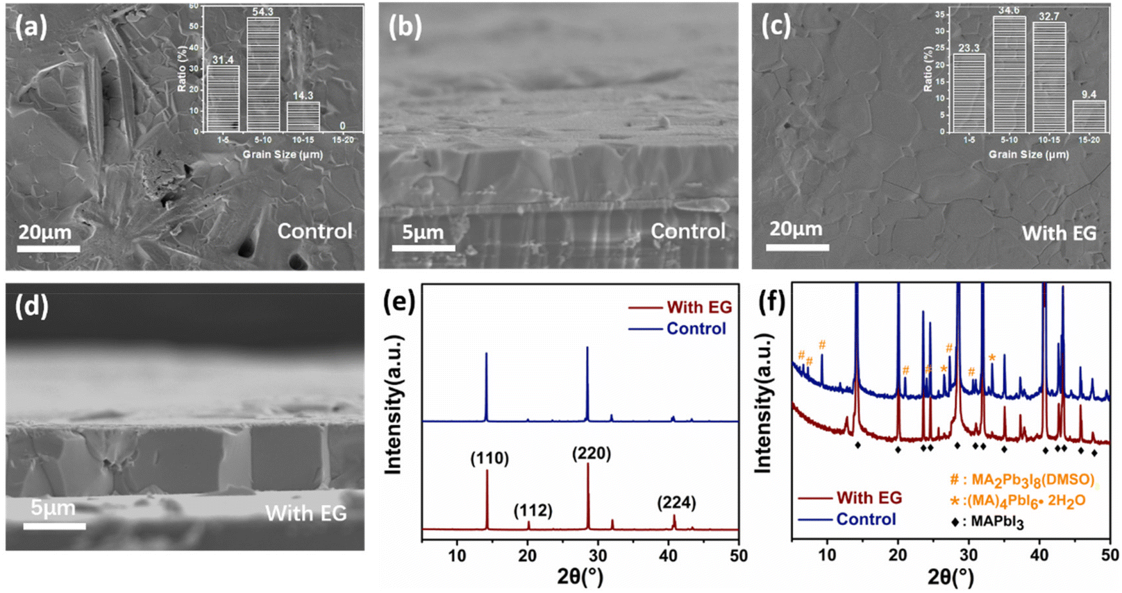 | ||
| Fig. 1 Top-view and cross-sectional SEM images of the control (a and b) and experimental sample (c and d). (e and f) The XRD patterns of the control and experimental sample. These perovskite films were all deposited on FTO. | ||
There have been many reports in the literature that, during the crystallization of the perovskite materials, some rod-like mesophase compounds may remain on the perovskite film surface. To explore this possibility, the crystal structure of the perovskite films was characterized by XRD. As shown in Fig. 1f, the XRD patterns suggest the presence of a number of the perovskite mesophase moieties in the control sample, including the lead rich MA2Pb3I8(DMSO)2 mesophase and the lead poor MA4PbI6(H2O)2 mesophase.46–49 The elemental analysis of the rod-like regions by EDS (energy dispersive spectroscopy) also showed that the I/Pb ratio was lower as compared to other regions (Fig. S4†). According to the literature,46–49 these mesophases often have a rod-like morphology, which is in line with our SEM observations. On the contrary, the experimental sample showed a uniform surface composition. It was noticed that the characteristic XRD peaks of the mesophase structures of the control sample were much weaker than the MAPbI3 peaks (Fig. 1f). This is reasonable given that such a rod-like mesophase could only exist on the surface of the perovskite film as concluded above.
The two kinds of perovskite films have very strong characteristic diffraction peaks of MAPbI3 at (110) and (220), which are indicative of the strongly preferred orientation of the MAPbI3 polycrystalline films (Fig. 1e). However, the full width at half maximum (FWHM) of the (110) diffraction peak (0.06°) for the experimental sample was lower than that for the control sample (0.11°). This phenomenon suggests that the crystal grain size of the perovskite film prepared with the ethylene glycol additive was larger than that of the control film. The differences of the two kinds of the perovskite films indicate that the addition of ethylene glycol could considerably affect the surface properties and crystalline quality of the perovskite films.
3.2 Mechanism of the additive effect
Further studies were carried out to reveal the mechanism of the additive effect on the perovskite film properties. Firstly, owing to its high boiling point 197.3 °C, ethylene glycol could possibly remain in the perovskite film during the ALS process. However, our NMR results ruled out this possibility. For the NMR testing, the perovskite film of the experimental sample was dissolved in the DMSO solvent (Fig. S5†), and no characteristic peak of ethylene glycol was found (the methylene peak was generally between 3–4 ppm). Therefore, ethylene glycol should only play a substantive role in the crystallization process and then volatilize completely after the annealing process.It is worth noting that ethylene glycol can dissolve MAI but can hardly dissolve lead iodide. This fact raised another possibility that the role of ethylene glycol was similar to the alcohol often used as an anti-solvent in the spin coating method. To uncover the influence of ethylene glycol on the crystallization of perovskite in the ALS process, an in situ microscopy system was built on a transparent hot plate to monitor the nucleation and crystallization process after the perovskite liquid membrane was formed by spraying (Fig. 2a–h) in ambient conditions. For the experimental sample, upon heating at 150 °C for about 31 s, the liquid membrane started to show a small amount of crystal nuclei, along with the solvent evaporation. The crystal nuclei continued to develop and about 7 s later, a full perovskite film was formed (Fig. 2d). For the control sample without ethylene glycol, however, the rod-like structures were immediately observed when the liquid membrane was just sprayed on the substrate (at 0 s). After about 30 s heating, a large number of crystal nuclei appeared and about 2 s later, the crystallization process quickly completed, but the rod structures did not transform into perovskite crystals (Fig. 2e–h).
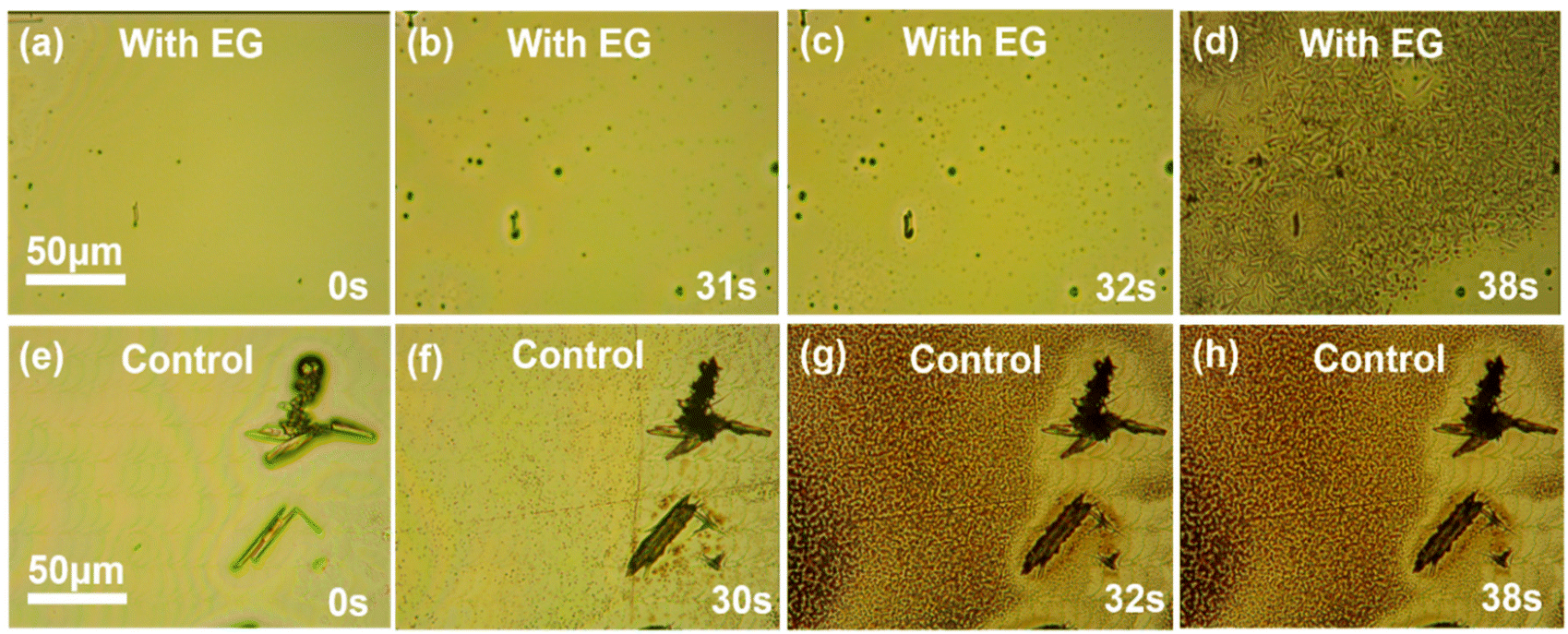 | ||
| Fig. 2 In situ optical microscopic images during the nucleation and crystallization process of the experimental sample at 0 s (a), 31 s (b), 32 s (c) and 38 s (d) and the control sample at 0 s (e), 30 s (f), 32 s (g) and 38 s (h). | ||
The above experimental results show that the nucleation and crystallization process of the perovskite changed significantly after the addition of ethylene glycol. Several points can be summarized here: (1) in the experimental sample, the nucleation rate was almost the same as in the control sample, but the inchoate grain density was far less than that of the control group (Fig. 2b and f); (2) the crystallization process in the experimental sample was slower than that in the control sample (Fig. 2c and d and 2g and h); and (3) after the precursor solution of the control sample was sprayed on the substrate, some large rod-like structures were formed immediately, but not at all in the experimental sample. In order to eliminate the influence of the ultrasonic spraying process, the spin coating method was used to prepare the corresponding perovskite wet films in ambient conditions. In situ optical microscopy images showed that a large number of rod-like structures still appeared in the control group but hardly any in the experimental group (Fig. S6†). This result is in accordance with that of the ALS method, ruling out that this structure is generated by the ultrasonic spraying process. Through the above analysis, from (1) and (2), we believe that the larger grain size of the perovskite film in the experimental group could be caused by the fewer nucleation sites and the slower crystallization rate. Also, from (3), the origin of the rod-structure could be inferred as follows. In fact, it has been reported previously that50,51 such rod-like structures originated from the interactions between the antisolvent molecules and the water molecules in air and perovskite precursors. These interactions and the formation of the complex intermediate phases were adverse to the ALS crystallization process or other solution methods for the perovskite film preparation in ambient air. Here, the ethylene glycol additive we used could be a magic bullet to fix this problem.
The preparation of the thick perovskite films by the solution method generally requires the deposition of thick liquid membranes for solid films fabrication after solvent volatilization or multi-step deposition method. No matter what method is adopted, it is necessary to obtain crystals with a large grain size and high crystal quality. Therefore, the right amount of nucleation sites in the crystallization process and full transformation of the mesophase is required when too many grain boundaries and defect sites are to be avoided. In this context, we have demonstrated that the addition of ethylene glycol could be a good solution to perfect perovskite films by modulating the corresponding nucleation and crystallization processes and thereby to significantly improve the photoelectric properties of the films.
3.3 Characterization of perovskite films
Next, optical and electrical characterizations were performed. Through the steady-state PL measurements on the surface of perovskite films, it can be seen that the photoluminescence peak positions of the two perovskite films were the same near 795 nm, which can be attributed to the intrinsic emission peak of MAPbI3. However, the photoluminescence of the perovskite films grown by the ALS process with ethylene glycol was significantly stronger than that of the control group. The change of the PL emission intensity was closely related to the recombination process inside the perovskite film. Some defect states on the surface of the perovskite film could induce substantial non-radiative recombination, leading to a reduction in the luminescence intensity (Fig. 3a).52,53 Therefore, the difference in the PL emission intensities suggests that the defect density on the surface of the experimental film sample was greatly reduced.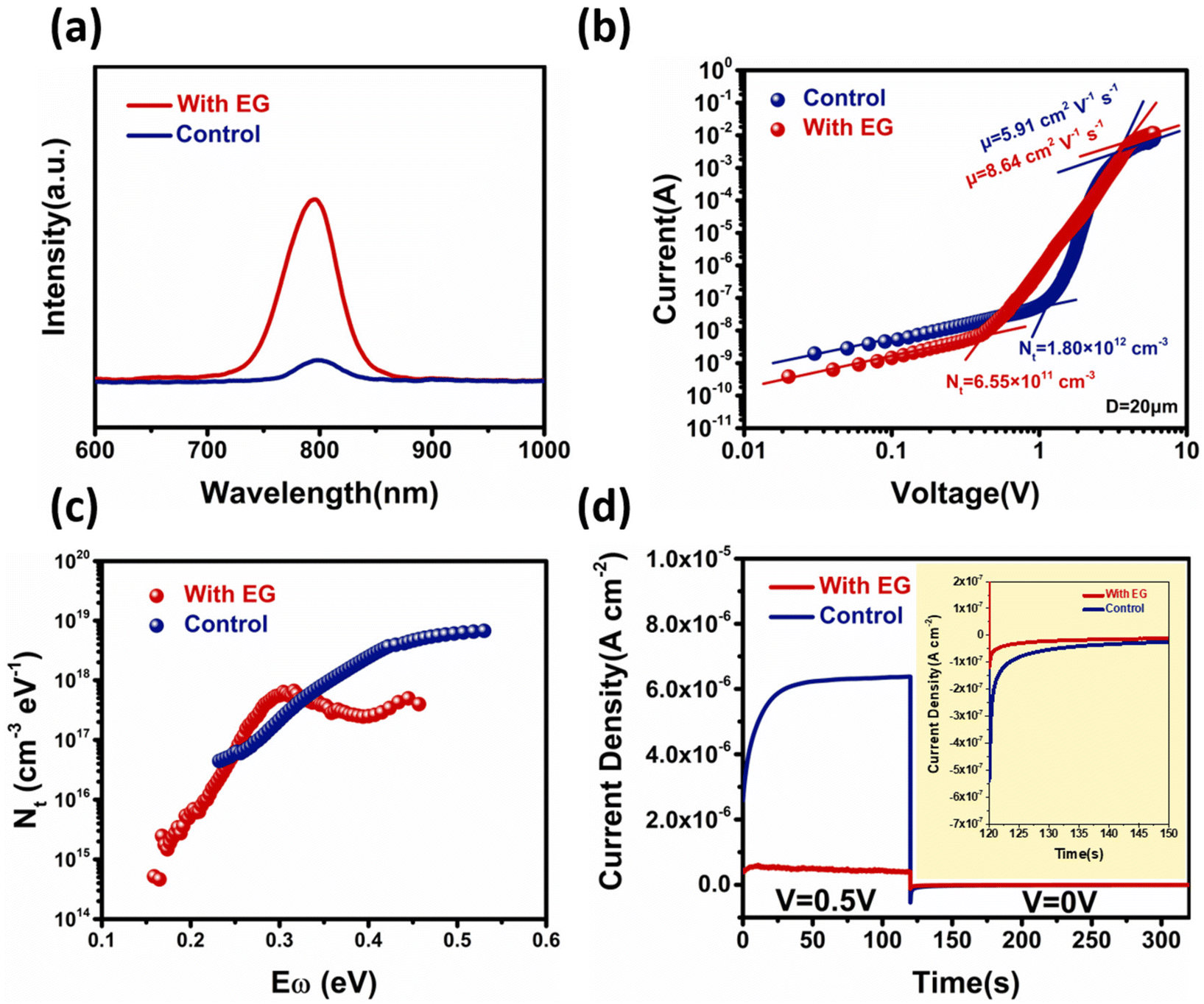 | ||
| Fig. 3 (a) PL signal of the MAPbI3 films (control and with EG). (b) SCLC measurements of the device with a structure of FTO/MAPbI3 (20 μm)/Carbon. (c) The trap density of states of the experimental and control sample obtained by thermal admittance spectroscopy. (d) The sample is first subjected to a bias to drive migration of the ions to the interfaces, followed by relaxation of the accumulated ions. | ||
To further investigate the defect density of two perovskite films, we carried out the space-charge-limited current (SCLC) and thermal admittance spectroscopy (TAS) measurements. The SCLC and TAS measurements were performed on the device structures of FTO/MAPbI3/carbon54 and FTO/NiOx/MAPbI3/PCBM/Ag,55 respectively. In Fig. 3b, the defect density was calculated from the transition voltage of the defect filling region. The perovskite film defect density for the experimental group was only 6.55 × 1011 cm−3, which was lower than that for the control group (1.80 × 1012 cm−3). By fitting the curves in the Child region, the carrier mobilities (μ) of the control and experimental perovskites were calculated to be 8.64 cm2 V−1 s−1 and 5.91 cm2 V−1 s−1, respectively. The TAS measurements further revealed the difference in the defect density and defect energy level for these two samples.56,57 As shown in Fig. 3c, for the experimental group, the defect state density at the deeper level (0.35–0.45 eV) was significantly lower than that for the control group. This result further indicates that ethylene glycol could regulate the crystallization process and reduce the deep-level defects in the perovskite films, which is beneficial for the detector applications.
The defects in the perovskite materials can also cause ion migration. The concentrations of the mobile ions in the two MAPbI3 films were measured by first applying a bias to the device with the FTO/MAPbI3/C structure to drive the mobile ions to the interfaces, followed by the relaxation of the accumulated ions.58,59 As shown in Fig. 3d, once the bias was removed, the device immediately showed a negative ionic current. By integrating the ionic current, we found that the experimental sample had a much lower charge density than the control devices. This result indicates that the experimental sample had a lower mobile ion concentration than the control sample. The lower defect density, lower mobile ion concentration, and higher mobility for the experimental sample could be ascribed to the EG-enhanced crystal quality.
3.4 Device performance
To assess the performance of the materials we developed above, we inserted a layer of them into a perovskite X-ray detector with a device structure of FTO/MAPbI3(100 μm)/C and subjected it to a series of standard characterizations. Under the electric field of 15 V mm−1, the response signals of the two detector devices under the X-ray exposure dose of 2.25 mGyair s−1 were measured (Fig. 4a). The photocurrent density of the X-ray detector in the experimental group was about 3.75 × 10⁻⁵ A cm−2, which is higher than that in the control group (3.46 × 10⁻⁵ A cm−2). The dark current of the experimental sample was reduced from 1.05 × 10⁻⁵ A cm−2 to 6.81 × 10⁻⁶ A cm−2. The J–V test also indicated that the experimental group had a lower dark current (Fig. 4b). Overall, the on/off ratio was much improved. The significant decrease of the dark current is ascribed to the decrease of the ionic conductivity, while the small increase of the photocurrent could be due to the decrease of deep level defects.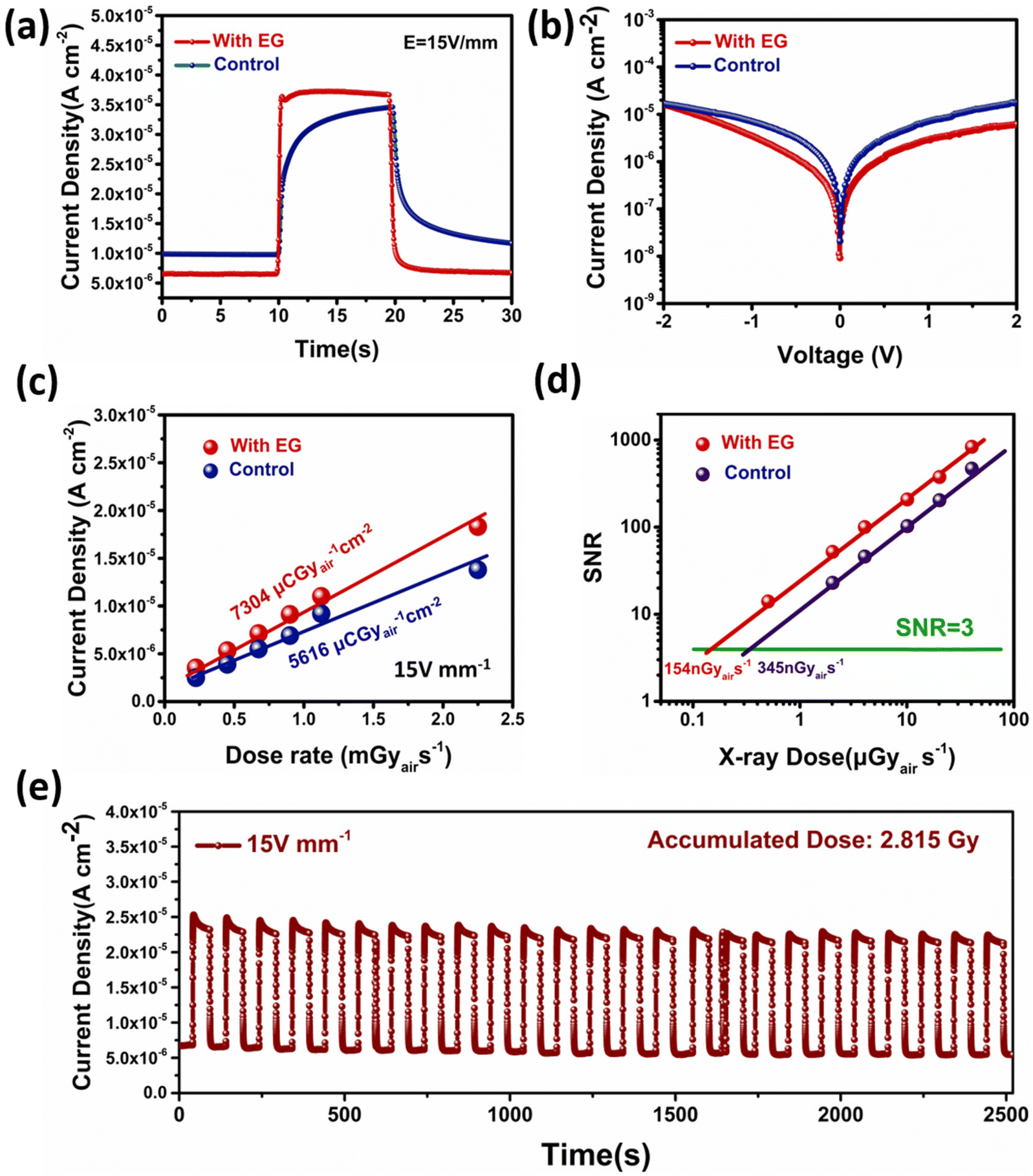 | ||
| Fig. 4 (a) The X-ray response profiles of the control and experimental detectors with a dose rate at 2.25 mGyair s−1 under 15 V mm−1. (b) J–V characteristics of the X-ray detectors. (c) The X-ray generated current density as a function of dose rate at different applied electrical fields. (d) The dose rate dependent SNR of the control and experimental detectors. (e) X-ray response stability of an experimental detector. | ||
More importantly, the photocurrent of the detector in the control group reached its steady state very slowly and did not stabilize even after 10 s of exposure. The rise and fall times of the experimental sample were measured to be about 200 ms and 360 ms, respectively. Notably, because the opening of the X-ray shutter had a 200 ms delay, the actual response of the X-ray should be faster. The deep-level defects at the perovskite interface could trap the carriers and change the injection barrier at the interface. This process might lead to an increase of the response time. However, the details about the defect types and mechanisms need to be further investigated in the future.
By varying the X-ray dose from 2.25 mGy s−1 to 0.225 mGy s−1 (Fig. S7†), the sensitivity of the perovskite X-ray detector in the experimental group was measured to be about 7304 μCGyair−1 cm−2 (Fig. 4c), which was higher than 5616 μCGy−1 cm−2 in the control group. As shown in Fig. S8,† this performance difference was statistically significant. The SNR (signal-to-noise ratio) of the detectors is plotted in Fig. 4d as a function of the dose rate. The SNR showed a good linear dependence on the dose rate and therefore, the LoD (limit of detection) could be obtained by extrapolating the SNR to the value of 3. The LoD was found to be reduced from 345 nGyair s−1 for the control detectors to 154 nGyair s−1 for the experimental detectors (Fig. S9†). We benchmarked the key parameters of our X-ray detectors with other reported detectors measured under similar test conditions (Table S1†) and we found that our detectors have higher sensitivity and lower LoD than most of the others.38,60–66
The stability of the perovskites used in our devices is important for the X-ray detection. To check this aspect, we measured the response of the detector under on–off X-ray radiation. The dark current and photocurrent of the MAPbI3 detector showed little degradation throughout the whole test period with an accumulated radiation dose of 2.815 Gy (Fig. 4e).
4 Conclusions
In this study, we revisited the solvent engineering strategy but on the ALS platform in order to deposit thick high-quality perovskite films in the ambient air for the X-ray detector applications. Previously, the MAPbI3 perovskite film grown by the ALS method suffered from a considerable number of defect sites and mesophase residues on the surface. We herein have identified ethylene glycol as an excellent quality-boosting additive for MAPbI3 perovskite films. In the mechanistic study, ethylene glycol was found to inhibit the generation of the perovskite mesophase by primarily curbing the effect of ambient air with high humidity, reduce the number of nucleation in the nucleation process, and slow down the crystallization rate in the crystallization process, which could effectively reduce the defects of the perovskite film especially on the surfaces. The X-ray detector applications taking advantage of the afforded materials were further demonstrated with much improved performance. The sensitivity of the detectors was promoted from 5616 μCGyair−1 cm−2 to 7304 μCGyair−1 cm−2. Their dark current density was reduced from 1.05 × 10⁻⁵ A cm−2 to 6.81 × 10⁻⁶ A cm−2 and the response speed was also faster. This work provided a simple effective strategy to process high-quality thick perovskite films for the direct X-ray detector applications.Conflicts of interest
There are no conflicts to declare.Acknowledgements
This work was supported by the National Natural Science Foundation of China (22261160370, U2001217, 21972006 and 22175005), Guangdong Basic and Applied Basic Research Foundation (2020B1515120039), Shenzhen Peacock Plan (KQTD2016053015544057) and Shenzhen Innovation Fund (JCYJ20220818101018038).References
- J. M. Kadro and A. Hagfeldt, Joule, 2017, 1, 29–46 CrossRef.
- N. Li, X. Niu, L. Li, H. Wang, Z. Huang, Y. Zhang, Y. Chen, X. Zhang, C. Zhu, H. Zai, Y. Bai, S. Ma, H. Liu, X. Liu, Z. Guo, G. Liu, R. Fan, H. Chen, J. Wang, Y. Lun, X. Wang, J. Hong, H. Xie, D. S. Jakob, X. G. Xu, Q. Chen and H. Zhou, Science, 2021, 373, 561–567 CrossRef CAS PubMed.
- Y. Zhao, F. Ma, Z. Qu, S. Yu, T. Shen, H. X. Deng, X. Chu, X. Peng, Y. Yuan, X. Zhang and J. You, Science, 2022, 377, 531–534 CrossRef CAS PubMed.
- Y. Cao, N. Wang, H. Tian, J. Guo, Y. Wei, H. Chen, Y. Miao, W. Zou, K. Pan, Y. He, H. Cao, Y. Ke, M. Xu, Y. Wang, M. Yang, K. Du, Z. Fu, D. Kong, D. Dai, Y. Jin, G. Li, H. Li, Q. Peng, J. Wang and W. Huang, Nature, 2018, 562, 249–253 CrossRef CAS PubMed.
- S. Yakunin, B. M. Benin, Y. Shynkarenko, O. Nazarenko, M. I. Bodnarchuk, D. N. Dirin, C. Hofer, S. Cattaneo and M. V. Kovalenko, Nat. Mater., 2019, 18, 846–852 CrossRef CAS PubMed.
- L. Shen, Y. Fang, D. Wang, Y. Bai, Y. Deng, M. Wang, Y. Lu and J. Huang, Adv. Mater., 2016, 28, 10794–10800 CrossRef CAS PubMed.
- T. Zhang, F. Wang, P. Zhang, Y. Wang, H. Chen, J. Li, J. Wu, L. Chen, Z. D. Chen and S. Li, Nanoscale, 2019, 11, 2871–2877 RSC.
- D. H. Kang, S. R. Pae, J. Shim, G. Yoo, J. Jeon, J. W. Leem, J. S. Yu, S. Lee, B. Shin and J. H. Park, Adv. Mater., 2016, 28, 7799–7806 CrossRef CAS PubMed.
- Z. Guo, Y. Wan, M. Yang, J. Snaider, K. Zhu and L. Huang, Science, 2017, 356, 59–62 CrossRef CAS PubMed.
- W. J. Yin, T. Shi and Y. Yan, Adv. Mater., 2014, 26, 4653–4658 CrossRef CAS PubMed.
- B. Li, D. Binks, G. Cao and J. Tian, Small, 2019, 15, 1–24 Search PubMed.
- D. K. Mohamad, J. Griffin, C. Bracher, A. T. Barrows and D. G. Lidzey, Adv. Energy Mater., 2016, 6, 1–7 Search PubMed.
- L. Li, Y. Chen, Z. Liu, Q. Chen, X. Wang and H. Zhou, Adv. Mater., 2016, 28, 9862–9868 CrossRef CAS PubMed.
- M. Liu, M. B. Johnston and H. J. Snaith, Nature, 2013, 501, 395–398 CrossRef CAS PubMed.
- Y. Deng, X. Zheng, Y. Bai, Q. Wang, J. Zhao and J. Huang, Nat. Energy, 2018, 3, 560–566 CrossRef CAS.
- N. G. Park and K. Zhu, Nat. Rev. Mater., 2020, 5, 333–350 CrossRef CAS.
- Z. Xiao, Q. Dong, C. Bi, Y. Shao, Y. Yuan and J. Huang, Adv. Mater., 2014, 26, 6503–6509 CrossRef CAS PubMed.
- K. Yan, M. Long, T. Zhang, Z. Wei, H. Chen, S. Yang and J. Xu, J. Am. Chem. Soc., 2015, 137, 4460–4468 CrossRef CAS PubMed.
- X. Cao, C. Li, Y. Li, F. Fang, X. Cui, Y. Yao and J. Wei, Nanoscale, 2016, 8, 19804–19810 RSC.
- F. Hao, C. C. Stoumpos, P. Guo, N. Zhou, T. J. Marks, R. P. H. Chang and M. G. Kanatzidis, J. Am. Chem. Soc., 2015, 137, 11445–11452 CrossRef CAS PubMed.
- J. C. Yu, D. W. Kim, D. B. Kim, E. D. Jung, K. S. Lee, S. Lee, D. Di Nuzzo, J. S. Kim and M. H. Song, Nanoscale, 2017, 9, 2088–2094 RSC.
- Y. Liu, Z. Xu, Z. Yang, Y. Zhang, J. Cui, Y. He, H. Ye, K. Zhao, H. Sun, R. Lu, M. Liu, M. G. Kanatzidis and S. Liu, Matter, 2020, 3, 180–196 CrossRef.
- Y. C. Kim, K. H. Kim, D. Y. Son, D. N. Jeong, J. Y. Seo, Y. S. Choi, I. T. Han, S. Y. Lee and N. G. Park, Nature, 2017, 550, 87–91 CrossRef CAS PubMed.
- J. A. Rowlands, Nature, 2017, 550, 47–48 CrossRef CAS PubMed.
- H. Wei, Y. Fang, P. Mulligan, W. Chuirazzi, H. H. Fang, C. Wang, B. R. Ecker, Y. Gao, M. A. Loi, L. Cao and J. Huang, Nat. Photonics, 2016, 10, 333–339 CrossRef CAS.
- S. Shrestha, R. Fischer, G. J. Matt, P. Feldner, T. Michel, A. Osvet, I. Levchuk, B. Merle, S. Golkar, H. Chen, S. F. Tedde, O. Schmidt, R. Hock, M. Rührig, M. Göken, W. Heiss, G. Anton and C. J. Brabec, Nat. Photonics, 2017, 11, 436–440 CrossRef CAS.
- S. Yakunin, M. Sytnyk, D. Kriegner, S. Shrestha, M. Richter, G. J. Matt, H. Azimi, C. J. Brabec, J. Stangl, M. V. Kovalenko and W. Heiss, Nat. Photonics, 2015, 9, 444–449 CrossRef CAS PubMed.
- W. Wei, Y. Zhang, Q. Xu, H. Wei, Y. Fang, Q. Wang, Y. Deng, T. Li, A. Gruverman, L. Cao and J. Huang, Nat. Photonics, 2017, 11, 315–321 CrossRef CAS.
- Y. Liu, Y. Zhang, X. Zhu, J. Feng, I. Spanopoulos, W. Ke, Y. He, X. Ren, Z. Yang, F. Xiao, K. Zhao, M. Kanatzidis and S. Liu, Adv. Mater., 2021, 33, 1–10 Search PubMed.
- S. Deumel, A. van Breemen, G. Gelinck, B. Peeters, J. Maas, R. Verbeek, S. Shanmugam, H. Akkerman, E. Meulenkamp, J. E. Huerdler, M. Acharya, M. García-Batlle, O. Almora, A. Guerrero, G. Garcia-Belmonte, W. Heiss, O. Schmidt and S. F. Tedde, Nat. Electron., 2021, 4, 681–688 CrossRef CAS.
- S. Yakunin, D. N. Dirin, Y. Shynkarenko, V. Morad, I. Cherniukh, O. Nazarenko, D. Kreil, T. Nauser and M. V. Kovalenko, Nat. Photonics, 2016, 10, 585–589 CrossRef CAS.
- Y. Liu, X. Zheng, Y. Fang, Y. Zhou, Z. Ni, X. Xiao, S. Chen and J. Huang, Nat. Commun., 2021, 12, 4–11 CrossRef PubMed.
- R. Zhuang, X. Wang, W. Ma, Y. Wu, X. Chen, L. Tang, H. Zhu, J. Liu, L. Wu, W. Zhou, X. Liu and Y. Yang, Nat. Photonics, 2019, 13, 602–608 CrossRef CAS.
- W. Qian, X. Xu, J. Wang, Y. Xu, J. Chen, Y. Ge, J. Chen, S. Xiao and S. Yang, Matter, 2021, 4, 942–954 CrossRef CAS.
- M. Xia, Z. Song, H. Wu, X. Du, X. He, J. Pang, H. Luo, L. Jin, G. Li, G. Niu and J. Tang, Adv. Funct. Mater., 2022, 32, 1–10 Search PubMed.
- W. Li, Y. Xu, J. Peng, R. Li, J. Song, H. Huang, L. Cui and Q. Lin, ACS Appl. Mater. Interfaces, 2021, 13, 2971–2978 CrossRef CAS PubMed.
- H. Tsai, S. Shrestha, L. Pan, H. H. Huang, J. Strzalka, D. Williams, L. Wang, L. R. Cao and W. Nie, Adv. Mater., 2022, 34, 2106498 CrossRef CAS PubMed.
- H. Mescher, F. Schackmar, H. Eggers, T. Abzieher, M. Zuber, E. Hamann, T. Baumbach, B. S. Richards, G. Hernandez-Sosa, U. W. Paetzold and U. Lemmer, ACS Appl. Mater. Interfaces, 2020, 12, 15774–15784 CrossRef CAS PubMed.
- J. Lin, M. Lai, L. Dou, C. S. Kley, H. Chen, F. Peng, J. Sun, D. Lu, S. A. Hawks, C. Xie, F. Cui, A. P. Alivisatos, D. T. Limmer and P. Yang, Nat. Mater., 2018, 17, 261–267 CrossRef CAS PubMed.
- J. K. Nam, M. S. Jung, S. U. Chai, Y. J. Choi, D. Kim and J. H. Park, J. Phys. Chem. Lett., 2017, 8, 2936–2940 CrossRef CAS PubMed.
- B. R. Sutherland, Joule, 2019, 3, 1–3 CrossRef.
- H. Zhang, F. Wang, Y. Lu, Q. Sun, Y. Xu, B. B. Zhang, W. Jie and M. G. Kanatzidis, J. Mater. Chem. C, 2020, 8, 1248–1256 RSC.
- C. Liu, Y. Yang, C. Zhang, S. Wu, L. Wei, F. Guo, G. M. Arumugam, J. Hu, X. Liu, J. Lin, R. E. I. Schropp and Y. Mai, Adv. Mater., 2020, 32, 1–9 Search PubMed.
- L. M. Herz, ACS Energy Lett., 2017, 2, 1539–1548 CrossRef CAS.
- Y. Liu, Y. Zhang, Z. Yang, D. Yang, X. Ren, L. Pang and S. F. Liu, Adv. Mater., 2016, 28, 9204–9209 CrossRef CAS PubMed.
- Y. Rong, S. Venkatesan, R. Guo, Y. Wang, J. Bao, W. Li, Z. Fan and Y. Yao, Nanoscale, 2016, 8, 12892–12899 RSC.
- Y. Bai, S. Xiao, C. Hu, T. Zhang, X. Meng, Q. Li, Y. Yang, K. S. Wong, H. Chen and S. Yang, Nano Energy, 2017, 34, 58–68 CrossRef CAS.
- Y. Guo, K. Shoyama, W. Sato, Y. Matsuo, K. Inoue, K. Harano, C. Liu, H. Tanaka and E. Nakamura, J. Am. Chem. Soc., 2015, 137, 15907–15914 CrossRef CAS PubMed.
- L. Zuo, S. Dong, N. De Marco, Y. T. Hsieh, S. H. Bae, P. Sun and Y. Yang, J. Am. Chem. Soc., 2016, 138, 15710–15716 CrossRef CAS PubMed.
- K. Zhang, Z. Wang, G. Wang, J. Wang, Y. Li, W. Qian, S. Zheng, S. Xiao and S. Yang, Nat. Commun., 2020, 11, 1–11 CrossRef PubMed.
- S. Xiao, K. Zhang, S. Zheng and S. Yang, Nanoscale Horiz., 2020, 5, 1147–1154 RSC.
- F. Zheng, X. Wen, T. Bu, S. Chen, J. Yang, W. Chen, F. Huang, Y. Cheng and B. Jia, ACS Appl. Mater. Interfaces, 2018, 10, 31452–31461 CrossRef CAS PubMed.
- G. Xing, N. Mathews, S. S. Lim, N. Yantara, X. Liu, D. Sabba, M. Grätzel, S. Mhaisalkar and T. C. Sum, Nat. Mater., 2014, 13, 476–480 CrossRef CAS PubMed.
- X. Xu, W. Qian, J. Wang, J. Yang, J. Chen, S. Xiao, Y. Ge and S. Yang, Adv. Sci., 2021, 8, 1–12 Search PubMed.
- J. Wang, S. Xiao, W. Qian, K. Zhang, J. Yu, X. Xu, G. Wang, S. Zheng and S. Yang, Adv. Mater., 2021, 33, 1–9 Search PubMed.
- S. Yang, S. Chen, E. Mosconi, Y. Fang, X. Xiao, C. Wang, Y. Zhou, Z. Yu, J. Zhao, Y. Gao, F. De Angelis and J. Huang, Science, 2019, 365, 473–478 CrossRef CAS PubMed.
- J. M. Ball and A. Petrozza, Nat. Energy, 2016, 1, 16149 CrossRef CAS.
- Y. Cheng, H. W. Li, J. Qing, Q. D. Yang, Z. Guan, C. Liu, S. H. Cheung, S. K. So, C. S. Lee and S. W. Tsang, J. Mater. Chem. A, 2016, 4, 12748–12755 RSC.
- Y. Zhao, C. Liang, H. Zhang, D. Li, D. Tian, G. Li, X. Jing, W. Zhang, W. Xiao, Q. Liu, F. Zhang and Z. He, Energy Environ. Sci., 2015, 8, 1256–1260 RSC.
- J. Li, X. Du, G. Niu, H. Xie, Y. Chen, Y. Yuan, Y. Gao, H. Xiao, J. Tang, A. Pan and B. Yang, ACS Appl. Mater. Interfaces, 2020, 12, 989–996 CrossRef PubMed.
- C. Ji, S. Wang, Y. Wang, H. Chen, L. Li, Z. Sun, Y. Sui, S. Wang and J. Luo, Adv. Funct. Mater., 2020, 30, 1905529 CrossRef CAS.
- W. Yuan, G. Niu, Y. Xian, H. Wu, H. Wang, H. Yin, P. Liu, W. Li and J. Fan, Adv. Funct. Mater., 2019, 29, 1900234 CrossRef.
- Z. Xu, X. Liu, Y. Li, X. Liu, T. Yang, C. Ji, S. Han, Y. Xu, J. Luo and Z. Sun, Angew. Chem., Int. Ed., 2019, 58, 15757–15761 CrossRef CAS PubMed.
- K. Tao, Y. Li, C. Ji, X. Liu, Z. Wu, S. Han, Z. Sun and J. Luo, Chem. Mater., 2019, 31, 5927–5932 CrossRef CAS.
- Y. Haruta, T. Ikenoue, M. Miyake and T. Hiratol, MRS Adv., 2020, 5, 395–401 CrossRef CAS.
- J. Guo, Y. Xu, W. Yang, B. Zhang, J. Dong, W. Jie and M. G. Kanatzidis, J. Mater. Chem. C, 2019, 7, 8712–8719 RSC.
Footnote |
| † Electronic supplementary information (ESI) available. See DOI: https://doi.org/10.1039/d2nr07016b |
| This journal is © The Royal Society of Chemistry 2023 |