
 Open Access Article
 This Open Access Article is licensed under a Creative Commons Attribution-Non Commercial 3.0 Unported Licence
Tuning the energy transfer in Ruddlesden–Popper perovskites phases through isopropylammonium addition – towards efficient blue emitters†
Martha Judith
Rivera Medina
 ab,
Lorenzo
Di Mario
a,
Simon
Kahmann‡
a,
Jun
Xi§
a,
Giuseppe
Portale
c,
Giovanni
Bongiovanni
d,
Andrea
Mura
d,
Juan Carlos
Alonso Huitrón
b and
Maria Antonietta
Loi
*a
ab,
Lorenzo
Di Mario
a,
Simon
Kahmann‡
a,
Jun
Xi§
a,
Giuseppe
Portale
c,
Giovanni
Bongiovanni
d,
Andrea
Mura
d,
Juan Carlos
Alonso Huitrón
b and
Maria Antonietta
Loi
*a
aPhotophysics & Optoelectronics group, Zernike Institute of Advanced Materials, University of Groningen, Nijenborgh 4, 9747 AG, Groningen, The Netherlands. E-mail: M.A.Loi@rug.nl
bDepartamento de Materia Condensada y Criogenia. Instituto de Investigaciones en Materiales. Universidad Nacional Autónoma de México. Ciudad Universitaria, A.P. 70-360, Coyoacán, 04510, Mexico City, Mexico
cMacromolecular Chemistry and New Polymeric Material, Zernike Institute for Advanced Materials, University of Groningen, Nijenborgh 4, 9747 AG Groningen, The Netherlands
dDipartimento di Fisica, Università degli Studi di Cagliari, cittadella universitaria 09040, Monserrato, Cagliari, Italy
First published on 13th March 2023
Abstract
Here we demonstrate blue LEDs with a peak wavelength of 481 nm, with outstanding colour purity of up to 88% (CIE coordinates (0.1092, 0.1738)), an external quantum yield of 5.2% and a luminance of 8260 cd m−2. These devices are based on quasi-2D PEA2(Cs0.75MA0.25)Pb2Br7, which is cast from solutions containing isopropylammonium (iPAm). iPAm as additive assist in supressing the formation of bulk-like phases, as pointed out by both photophysical and structural characterization. Additionally, the study of the excitation dynamics demonstrates a hindering of the energy transfer to domains of lower energy that generally undermines the performance and emission characteristics of blue-emitting LEDs based on quasi-2D perovskites. The achieved narrow distribution of quantum well sizes and the hindered energy transfer result in a thin film photoluminescence quantum yield exceeding 60%. Our work demonstrates the great potential to tailor the composition and the structure of thin films based on Ruddlesden–Popper phases to boost performance of optoelectronic devices – specifically blue perovskite LEDs.
Introduction
Metal halide perovskites (MHP) are hot contenders for the next generation of light emitters, especially for display technology.1 They show remarkable optical properties, such a high luminescence quantum yield, a higher colour purity2 compared to currently employed emitters and a colour tunability that offers a wide colour gamut (≈120%–140% above the NTSC CIE chromaticity standards).3,4 Moreover, facile solution-processable techniques allow for reducing fabrication costs.Light-emitting diodes based on MHPs (PeLEDs) have been extensively studied in the last few years. As a result, devices with exceptional external quantum efficiency (EQE) with electroluminescence in the green (as high as 28%),5–7 red (record above 25%),8,9 and infrared (20%) spectral range10,11 have been fabricated. But for blue-emitting PeLEDs, the progress in efficiency has been lagging behind, although many efforts have been dedicated to improving these devices.12–25 Recently, a record EQE of 17.9% has been reported by ligand manipulation in on-substrate synthesis of quantum dots.26
At least three major approaches have been used to fabricate efficient blue-emissive MHP layers with high values of photoluminescence quantum yields (PLQYs), which acts as a primary indicator for a promising emissive layers in emitting devices technology.27 These three approaches rely on the use of active layers of very different nature, namely: (i) 3D MHPs,15,25,28 (ii) quasi-2D perovskites,17,21,22,29,30 and (iii) nanocrystals based on 3D MHPs.16,23,31
The first approach has the advantage of the good charge transport properties of 3D perovskites, which contribute to improve the EQE. However, the PLQY is often limited in bulk materials, as it is affected by trap-induced and non-radiative recombination.25,28 Furthermore, to push the emission towards the blue spectral region, it is common to use Cl/Br mixtures, which are prone to phase separate in Cl-rich or Br-rich domains, leading to multiple emission peaks and unstable colour coordinates.15 In the last strategy, based on perovskites nanocrystals, the colour is primarily tailored by varying the halide composition, although also variation of the dimensionality of the system composing the nanostructure from 3D to 2D perovskites have been reported.33–35 This approach shows its potential with PLQY values higher than 80%,32 reached thanks to charge carrier confinement and when good ligand passivation is achieved. However, ligands at the surface are also detrimental for charge carrier transport because of their insulating nature, but removing them leads the crystal to fuse losing the confinement, which is already intrinsically weak. Therefore, to obtain PeLEDs with high EQE with this approach, a careful selection of the ligands is crucial and often challenging.16,23,31
In quasi-2D perovskites, the emission colour can be adjusted according to the dimensionality of the phases obtained upon the film formation. In general, thin films casted from solutions of a nominal stoichiometry (〈n〉) corresponding to a specific thickness of the layered inorganic octahedral slabs (for example n = 2), in reality will incorporate a wide array of domains of different dimensionality (n = 2,3,4,5,…) and band gap energies.36 The injected charge carriers can then funnel amongst the n-values from highest to lowest energy domain resulting in very high quantum yields.37 This relation between optical and structural-properties makes quasi-2D perovskites a promising candidate for light emission applications. Both Ruddlesden–Popper (RP)17,21,29,30,38 as well as Dion–Jacobson (DJ) phases,22,39,40 the two most common quasi-2D perovskites structures, already achieved remarkable performance in blue-emitting PeLEDs with record EQE above 15%.21,22 RP phases are currently the most investigated, thanks to the more favourable formation energy of middle-n phases (such as n = 3) and the less efficient energy transfer from 2D to 3D phases, both key factors to obtain blue-emitting PeLEDs.41,42
The interesting properties of quasi-2D perovskites, and in particular of the RP phases, come with several challenges, as to control the phase distribution and their orientation to favour charge transport. In fact, the crystallisation process which undergoes the formation of quasi-2D perovskites is complex and still not fully understood, as solvents molecules, organic cations and precursor salts coexist giving rise to the presence of intermediate phases.43 Thus, depending on the solvent, the organic cations dispersibility and the nature of the intermediate phases, a different phase distribution and therefore the phase orientation will be obtained. Possible ways to address such challenges include careful procedures for solvent engineering,44–46 antisolvent methods,47 and the incorporation of additives.48
Additives have played an important role in the crystallisation of perovskite films, acting as passivating agents, and structural and optical modifiers.49–53 For quasi-2D, phenyl-based amines are predominantly used as spacer cations as they provide rigidness to the structure. The introduction as additives of alkyl chain organic amines cations can further assist in controlling the phase distribution.54–56 Fine-tuning of the optoelectronic properties can be achieved by adequately selecting the size of the alkyl chain. The length of the alkyl chain can build up intermolecular interactions, which may become a barrier for carrier transport. Branched spacer cations have proved to increase crystallinity of the quasi-2D phases and their orientation with enhanced charge transport properties.57
This work reports the fabrication of LEDs using quasi-2D perovskites to achieve bright blue electroluminescence by incorporating the small branched alkyl amine cation iPAm (isopropylammonium) as an additive to the nominal 〈n〉 = 2 phase of composition PEA2(Cs0.75MA0.25)n−1PbnBr3n+1. By adding iPAm, we achieve blue emission with a PLQY of 64% when the active layer is deposited on the hole transporting layer PEDOT:PSS. Optical and structural investigations unveiled that the crystallisation of our RP phases is favoured for n = 3 perovskite crystallites embedded in a randomly oriented matrix of higher dimensional RP domains. This promotes efficient transport of charges towards domains of lower n-values, where they radiatively recombine. Interestingly, the energy transfer mechanism is inhibited by the use of iPAm. As a result, the champion PeLED fabricated reached an EQE of 5.2% with an EL peak at 481 nm and a high luminance of 8260 cd m−2. While these values are not record for this colour and class of materials, we provide a deep investigation of the optical and structural properties of the active layer that can be of guidance to further improve the optoelectronic properties of quasi-2D perovskites.
Results and discussion
To obtain blue-light emission we fabricated by spin-casting (using toluene as antisolvent) quasi-2D films of PEA2(Cs0.75MA0.25)n−1PbnBr3n+1 varying the nominal n phase (〈n〉); see Experimental section for details. We added isopropylammonium bromide (iPAm) to the precursor solutions, with the aim of controlling the phase distribution in the films. A schematic of the 〈n = 2〉 phase for neat and iPAm-modified films is proposed in Fig. 1(a).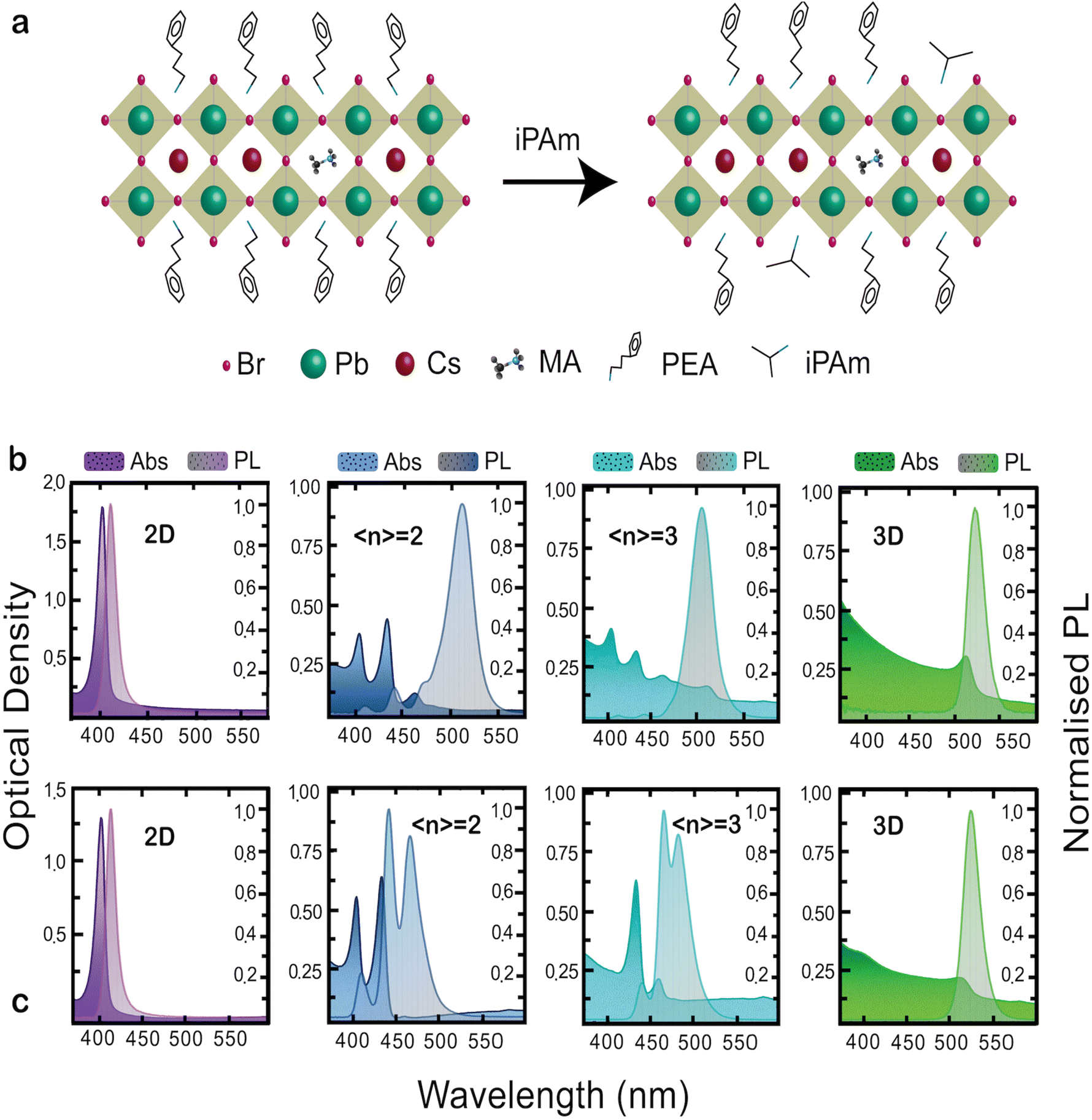 | ||
| Fig. 1 (a) Schematic illustration of our perovskite 〈n〉 = 2 RP phases system used as active layer of the blue PeLED. On the left side is depicted the composition PEA2(Cs0.75MA0.25)Pb2Br7 [neat] and on the right side the composition PEA2(Cs0.75MA0.25)Pb2Br7:iPAm obtained using isopropylammonium (iPAm) as additive. Steady-state optical characteristics of 3D (Cs0.75MA0.25PbBr3), 2D (PEA2PbBr4), and quasi-2D perovskites deposited on quartz substrates. Absorbance and photoluminescence (PL) spectra of thin films of different nominal 〈n〉 value for neat (b) and iPAm-modified (c) perovskite systems. PL spectra excitation wavelength is 267 nm. | ||
Fig. 1(b and c) depicts the absorption and photoluminescence spectra of 2D (n = 1; PEA2PbBr4), the 〈n〉 = 2 and 〈n〉 = 3 RP phases, and the 3D perovskite (Cs0.75MA0.25PbBr3) deposited on quartz substrates. In Fig. 1b the absorbance and PL spectra of the neat system are displayed. The spectra of the 2D sample, with an absorption peak at 403 nm and emission peak at 410 nm, are dominated by the excitonic features determined by dielectric and quantum confinement of carriers into the inorganic layers. The quasi-2D RP phases 〈n〉 = 2 and 〈n〉 = 3 show multiple peaks indicating the simultaneous presence of different phases in the thin film. The 〈n〉 = 2 thin film shows, together with the 2D phase (n = 1), the n = 2 and n = 3 phases with absorption and emission peaks located at 433 nm and 441 nm for the former and 464 nm and 475 nm for the latter. The absorbance spectrum shows a low energy tail indicating the presence of a small amount of material of larger n-values (quasi-3D) in the film. The PL spectrum is dominated by emission at 512 nm (note the 3D phase absorbance is located around 520 nm with an emission at 530 nm). The comparison between absorbance and PL spectra hints to an effective energy transfer (funnelling), from higher to lower energy phases, as the absorbance is dominated by the n = 2 phase, while the PL is mainly governed by the quasi-3D phases. Similarly, for the 〈n〉 = 3 thin film, we can observe the coexistence of the 2D, the n = 2, and of quasi-3D phases (peak at 516 nm) in the absorbance spectrum; whereas the PL is practically dominated by a broad emission ascribed to the quasi-3D phase.
Fig. 1c shows the absorption and PL properties of the iPAm samples. Interestingly, while the addition of iPAm does not seem to have a significant influence on the 2D sample and only a slight 5 nm blue-shift for both absorbance and PL on the 3D sample is observable, it has significant effect on the RP phases of 〈n〉 = 2 and 〈n〉 = 3, where an almost total suppression of larger n contributions and a significant diminishment for the 2D phase, are observed. The suppressed formation of quasi-3D phases (as exhibited from absorption) is extremely important, as it allows avoiding energy transfer and therefore the achievement of blue photoluminescence in the 423–507 nm range for the system with 〈n〉 = 2 and 〈n〉 = 3.
Aiming at fabricating LEDs, it is important to note that the perovskite emission layer will not be deposited on quartz, but on a hole transport layer (HTL). Different surface materials will lead to different wetting, which in turn has a strong impact not only on the structure and crystallisation of deposited films, but also on the energy landscape of RP phases.58,59 In our case, the perovskite layers of finished devices will be deposited onto a HTL which is poly(3,4-ethylenedioxythiophene) polystyrene sulfonate (PEDOT:PSS).60 It is therefore imperative to investigate the optical and structural properties of our perovskite films when deposited on PEDOT:PSS.
Hence, we first analyse the PL behaviour of our nominal 〈n〉 = 2 thin films for the neat and iPAm system when deposited on ITO/PEDOTS:PSS substrates (further referred to as PEDOT substrate). By comparing the PL for the neat system deposited on quartz and PEDOT (Fig. 2a), we observed no significant shift between the emissions from the samples except for an enhancement of the intensity of emission of lower n-phases. Upon adding iPAm (Fig. 2b), in the sample on PEDOT the n = 4 phase is favoured with an emission of 491 nm, while for the sample on quartz the n = 3 phase, with an emission at 475 nm, is the dominant. Consistently, with what observed for the neat system, iPAm samples show an increase in the relative intensity of emission from lower n-phases. Comparing the neat system with the one where iPAm is added on PEDOT (Fig. 2c), the emission from n = 2 and n = 3 phases is remarkably higher in the latter system. In contrast, the emission from n = 1 phase is diminished. Most importantly, the photoluminescence quantum yield (PLQY) of the films deposited on PEDOT (Fig. 2d) amount to about 60% for the iPAm samples, which is twice the neat film value. Notably, PLQYs for samples deposited on quartz do not overcome values of 7.2%.
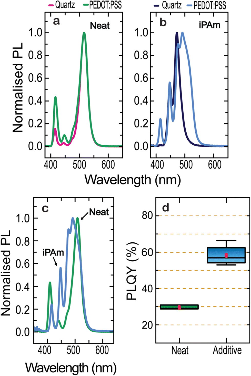 | ||
| Fig. 2 Photoluminescence characteristic of 〈n〉 = 2 thin films deposited on quartz and PEDOT of the (a) neat system (b) and the iPAm system, (c) comparison of both systems when deposited on PEDOT, and the (d) PLQYs of 12 samples of iPAm and neat thin films. | ||
To further understand the energy transfer mechanism in our 〈n〉 = 2 systems on PEDOT, we proceed to investigate the charge carrier dynamics with time-resolved PL (TRPL). Fig. 3a displays the TRPL spectra for the neat system. It is observed that shortly after the excitation, two high-intensity emissions arise from n = 1 and n = 2 phases, together with a broad emission located at 510 nm, which is the result of the overlapped emissions from n = 3, n = 4, and n ≥ 5 phases. By comparing the spectra at different time intervals after the excitation, the peaks assigned to the low values of n-phases undergo a rapid decay. On the contrary, the broad emission at 510 nm decays more slowly and it remains strong for entire time range investigated.
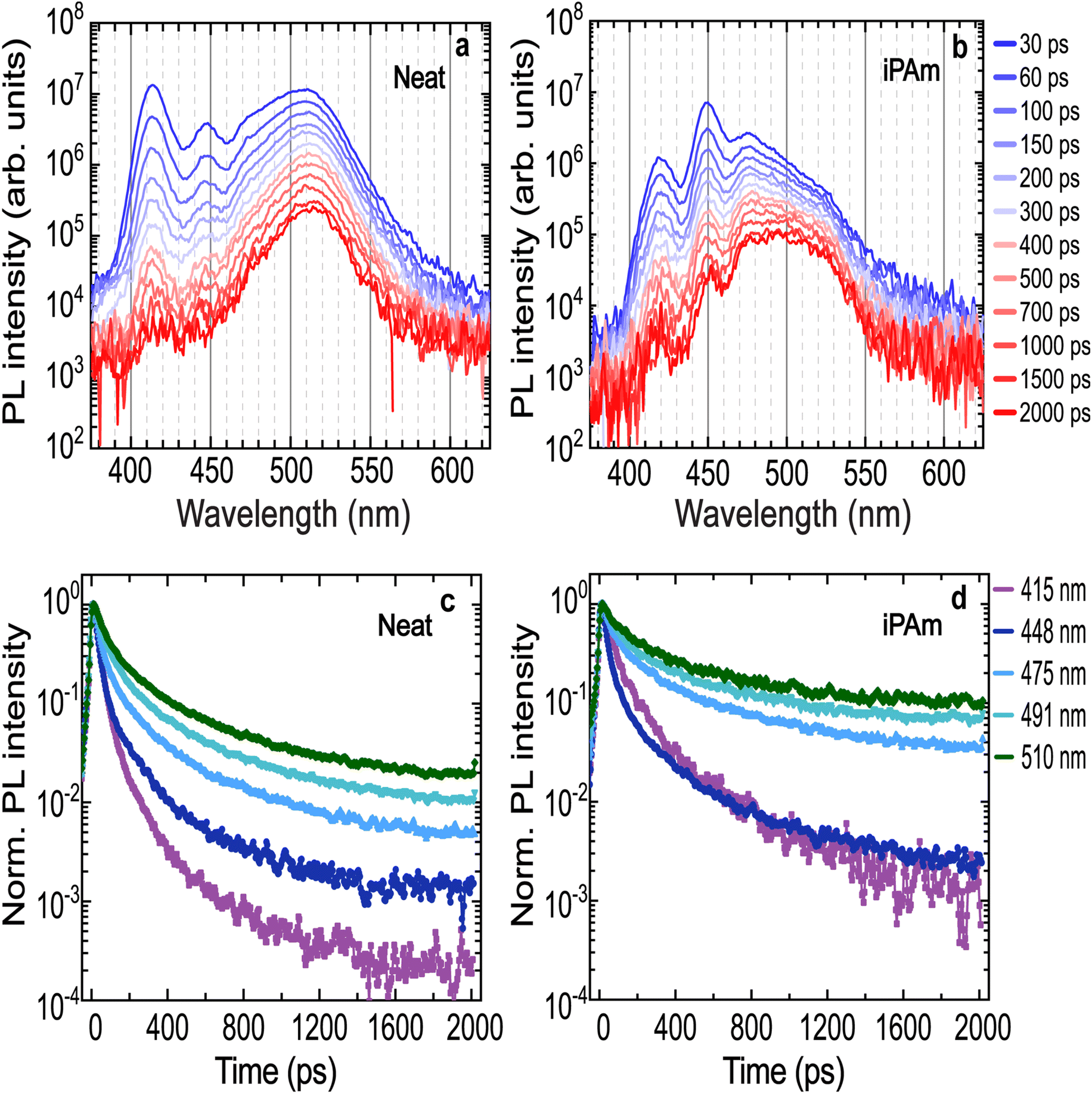 | ||
| Fig. 3 Time-resolved photoluminescence (TRPL) of 〈n〉 = 2 thin films deposited on PEDOT. PL spectra at different times after excitation of (a) neat system and (b) iPAm system. PL decays measured at different wavelengths, corresponding to the emission of different n-phases, in (c) neat system and (d) iPAm-modified thin films. | ||
The decays of the PL (Fig. 3c) are reported at the wavelengths corresponding to the peak positions extracted from the steady-state spectra (see Table S1†).
The decay dynamics were fitted using a multi-exponential function. The obtained PL lifetimes are reported in the ESI Table S2.† The lifetimes increase with higher n-phases values, both in the time range of tens and hundreds of picoseconds. Additionally, the n ≥ 5 phase emission is characterised by the slowest decay, with calculated lifetimes almost two-fold those of the emission of the other n-phases. While this behaviour seems to indicate energy transfer from the phases with larger bandgaps to the one with narrower bandgaps, which eventually ends in radiative recombination of the carriers in the n ≥ 5 phases, we have also to remember that low dimensional RP phases show normally a shorter lifetime than, for example, the 3D MHP.
For the iPAm system (Fig. 3b), despite an initial rapid decay, the emissions from n = 1 and n = 2 phases remain distinctly visible in the spectra up to 2 ns. Moreover, the PL broadband, which includes the emissions from n = 3, n = 4, and n ≥ 5 phases, at short times after the excitation, appears peaked at 475 nm, showing a dominant contribution of the n = 3 phase. Overall, the profile still shows components at high energy as if the energy funneling is partially hindered. This is a distinct behaviour from that observed in the neat system.
Driving our attention to the decay dynamics of the iPAm system (Fig. 3d), an increase in the PL lifetimes is evident for all the phases. The lifetimes are reported in Table S2.† Not only the emission from n = 1 and n = 2 for the iPAm-modified film is substantially longer than in the neat film, but also, the lifetime of emission from the n = 3, n = 4 and n ≥ 5 phases is significantly longer with lifetimes of tens or even hundreds of picoseconds.
In short, the analysis of the TRPL behaviour points out that the addition of iPAm to the RP 〈n〉 = 2 films, increases the PL lifetimes for all phases. This is in good agreement with the high values of PLQY observed for the system with iPAm. An increase in the PL lifetime could be explained by a hindering of the energy transfer but also by a reduction of non-radiative recombination, both possible effects of the addition of iPAm.
To better understand the effects of iPAm on the photophysics of the material, we performed fast-transient transmission spectroscopy measurements (FTTS) on both systems. Following the absorbance spectra shown above, the transient spectra of the neat system (Fig. 4a) show several photobleaching features in the range of wavelengths between 400 and 500 nm, result of the depopulation of the ground state of the different n-phases. The transient spectra evidence a rapid decay dynamic for the photobleaching associated with n = 1, n = 2, n = 3, and n = 4 phases (signals located at 403, 432, 462, and 480 nm, respectively), whereas the signal related to n ≥ 5 (507 nm) has a much longer lifetime, analogous to what we observed in the TRPL results.
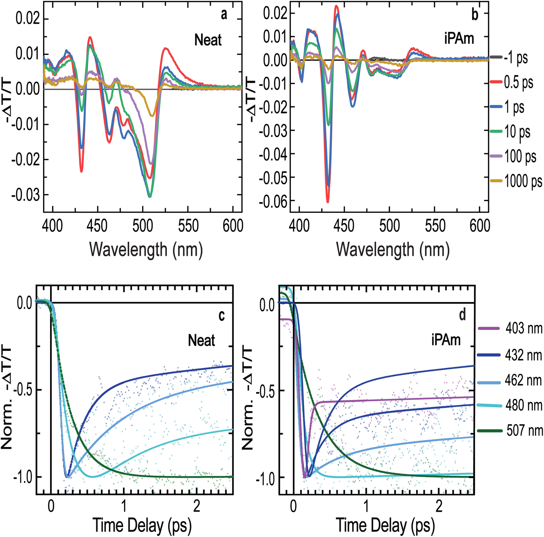 | ||
| Fig. 4 Fast transient transmission spectroscopy (FTTS) characterisation of 〈n〉 = 2 thin films deposited on PEDOT:PSS. Transient spectra at different delay times between pump and probe for (a) the neat system and (b) the iPAm system. Time dependence of the normalized FTAS signal at different wavelengths, corresponding to the main absorption bleaching features on the spectra, for (c) neat and (d) iPAm systems. The experimental data (coloured dots) and best fitting models (coloured lines). | ||
The decay dynamics of the transient transmission can be fitted by a multi-exponential function. The resultant fits are displayed in Fig. 4c and the extracted values are reported in ESI Table S3.† The dynamics of the transmission related to n = 1 phase (403 nm) was not possible to fit due to its extremely fast decay and the overlap with a much stronger photoinduced absorption feature. The photobleaching features related to n = 2 and n = 3 phases (432 and 462 nm, respectively) have both an initial fast decay, which halves the intensity of the signals in the time scale of hundreds of femtoseconds.
The decay dynamics for the n = 4 phase is similar, except for two noteworthy differences. First, the signal does not experience a sharp rising as the previous ones. It reaches its maximum in a time of hundreds of femtoseconds, which adequately corresponds to the initial fast decay of the former two signals. Second, the decay dynamics of this signal is much slower than the one of the low dimensional phases. The photobleaching signal associated with n ≥ 5 phases displays an even longer rise time than n = 4 and the decay dynamics is in the nanosecond regime. Therefore, the ultrafast decays for the signals related to low n-values and the rising in the signals associated with high n-values demonstrate an efficient energy transfer mechanism in the neat system.42,61,62
Conversely, the iPAm system exhibits higher intensities of the photobleaching signals for the low n-values, and their decay is significantly slower than in the neat system, as shown in Fig. 4b and d. The higher intensity suggests a more considerable amount of the related phases present in the sample, or a hindering of the ultrafast decay processes.
The effects of the addition of iPAm are clearly observed in the fit of the dynamics of the signals (Fig. 4d). While the initial fast decay of the signals associated with n = 1, n = 2, and n = 3 phases remain present, its impact on the intensity of the signals is largely reduced. Most of the photobleaching signal decays in the time range of a few nanoseconds, compatible with the radiative recombination for all these phases. The effects of the additive are highly pronounced on the n = 4 phase signal. After the rising, we do not observe further fast decay as if the energy funnelling towards higher values of n-phases is completely hindered. Lastly, the photobleaching related to the n ≥ 5 phases is still characterised by a noticeable rising, followed by prolonged decay longer than the neat system (and longer than the probed time range of 8 ns). However, it is important to underline that in this sample the n ≥ 5 phases are extremely weak as is evident from Fig. 4b and 2c. These results prove a substantial hindering of the energy transfer and thus a higher possibility of radiative recombination of the excitons in the phases, where they are generated. This is expected to enhance quantum yields and colour purity of the emission in light-emitting devices.
Having established the strong impact of iPAm on the optical characteristics of quasi-2D MHP thin films, we shift our focus towards structural aspects. Scanning electron microscopy images presented in Fig. 5a and b highlight strong differences in the morphology of the films. The neat system displays a wrinkled structure, whereas the iPAm system exhibits a smooth surface composed of small and randomly oriented flat crystallites, as furthermore revealed by atomic force microscopy (AFM) (ESI Fig. S4†). We expect the smooth film with uniform morphology induced by iPAm can promote an enhanced charge carrier transport.
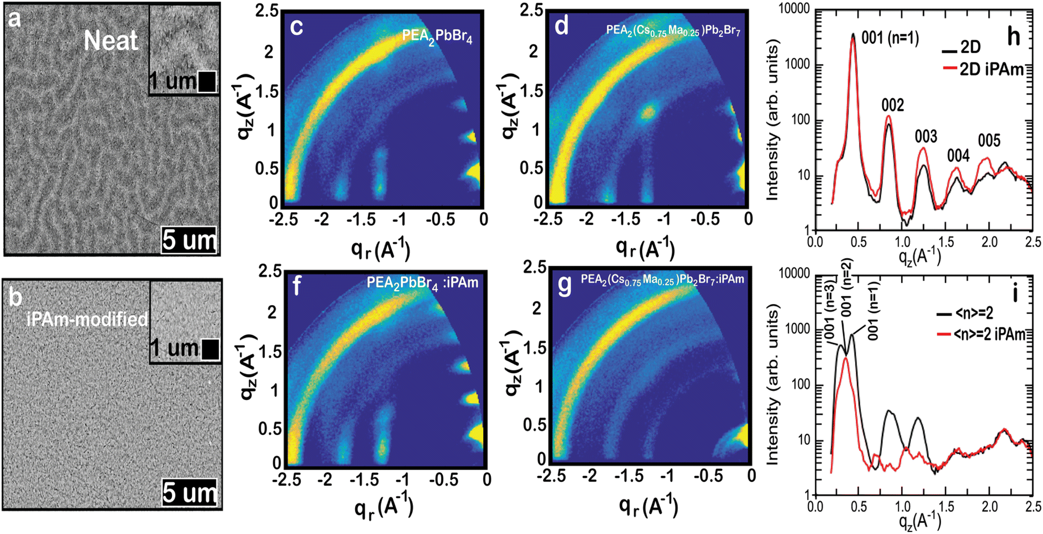 | ||
| Fig. 5 SEM micrographs of (a) 〈n〉 = 2 neat system and (b) 〈n〉 = 2 iPAm system. The inset shows a magnification of the surface. GIWAXS patterns of the neat system for (c) 2D control-perovskite and (d) 〈n〉 = 2 samples and GIWAXS patterns of the iPAm system for (f) 2D control-perovskite and (g) 〈n〉 = 2 samples. Comparison of the GIWAXS intensity cuts along the quasi vertical qz direction for the (h) 2D control-perovskite and (i) 〈n〉 = 2 samples with and without the iPAm addition. All films were deposited on PEDOT. | ||
To understand whether the formation of crystallites in the iPAm system deposited on PEDOT is due to a structural change during the perovskite film formation, we have performed powder-XRD characterisations for both systems when they are grown on either quartz or PEDOT. Moreover, we have performed the same characterisation to control samples, namely the 2D RP phases (n = 1). In general, no significant perturbation is observed for the 2D control-systems after the addition of iPAm, except for the emergence of two diffraction peaks when deposited on PEDOT (Fig. S5† and text therein). The 〈n〉 = 2 sample shows the coexistence of 2D and 3D phases with a clear dominance of the former after incorporating iPAm on quartz. Nonetheless, a particular situation occurs when this film is grown on PEDOT. It seems that the film has very low crystallinity with the emergence of a broad feature and a weak diffraction peak located a low value of 2-theta (see Fig. S5d†).
The puzzling XRD results called for further investigation. Therefore, the crystal structure of the neat and iPAm system deposited on PEDOT were further investigated by using 2D grazing-incidence wide-angle X-ray scattering (GIWAXS) (Fig. 5c–g). Despite of its lower resolution, GIWAXS is better suited than powder-XRD to gain a complete picture of quasi-2D perovskites in thin film structure, which tend to crystallise with multiple RP phases with certain orientation. The GIWAXS patterns allow for obtaining information about the packing adopted by the material and the preferred orientation of the perovskite crystallites.36,63,64 The GIWAXS pattern of the 2D neat system (PEA2PbBr4) can be described assuming a unit cell with a, b, and c axis of 12 × 12.5 × 17.5 Å in agreement with the powder-XRD results and the reported crystal structure for PEA2PbBr4.65 The 00l peaks are highly aligned along the quasi-vertical z-direction (see Fig. 5h), indicating that the 2D crystallites align with the 00l planes parallel to the substrate. This behaviour has been already reported for other 2D Pb- and Sn-based perovskites using PEA cations.36,66 The film shows a high degree of order as up to 5 00l reflections are visible along the z-direction. The addition of iPAm to the 2D neat system does not significantly alter the structure but increases the order slightly as the 00l reflections (with l > 1) are generally more intense and the 005 peak is more evident (see Fig. 5f).
As expected from the optical results, inspection of the intensity cuts along the qz direction reveals the simultaneous presence of different n-phases for the 〈n〉 = 2 neat system (PEA2(Cs0.75MA0.25)Pb2Br7), with n = 1 and n = 3 being the most abundant phases (Fig. 5i). Similar to the 2D phase, the 〈n〉 = 2 neat film is composed of crystallites strongly oriented with their 00l planes parallel to the substrate (see Fig. 5d). Contrary to what was observed for the 2D film, the addition of iPAm strongly alters the 〈n〉 = 2 phase structure. Two main effects are observed when iPAm is added to the 〈n〉 = 2 system: first, a change in the relative composition of the different phases is detected, as revealed by the change in the 001-peak intensity along the qz direction in Fig. 5i. Adding iPAm causes a decrease in the n = 1 and n = 3 phases, as previously observed in the PL data. Second, a significant increase of the fraction of the crystallites with a random orientation upon the addition of iPAm is observed from the appearance of the Debye–Sherrer rings in the GIWAXS pattern of Fig. 5f.
This change in orientation is expected to have a profound effect in the device performance. It has been reported that crystallites with random orientation can improve the charge transport in the direction perpendicular to the perovskite film; consequently, they may lead to higher efficiencies in light-emitting diodes.67 On the other hand, it has been shown that high orientation of a single phase can be beneficial to enhance the radiative recombination of the carriers.62
PeLEDs with 〈n〉 = 2 emission layers were fabricated using a device structure composed of ITO/PEDOT:PSS(35 nm)/〈n〉 = 2 perovskite (125 nm)/TPBi (40 nm) LiF (1 nm)/Al (80 nm), as depicted schematically in Fig. 6a. The details of the device fabrication process can be found in the Experimental section. The energy level alignment of the different materials composing the device and the carrier pathway are shown in Fig. 6b. The energy alignment of our emissive perovskite layer was estimated according to previous reports on bromide-based multi-cation quasi-2D perovskites.14,18,68 Electron are injected from a Li/Al top contact via a TPBi electron transport layer, while the holes are injected from the bottom ITO through PEDOT:PSS. It is important to underline that these energy levels are probably oversimplified as the composition of phases in the above-mentioned report is rather different than in our case. In case the estimation would be realistic, the energy diagram calls for a better HTL than PEDOT:PSS for this type of devices.
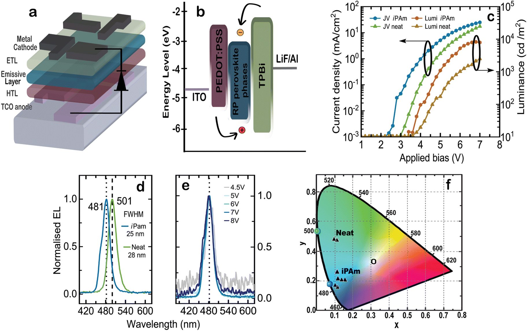 | ||
| Fig. 6 (a) Schematic illustration of the structure of our PeLED and (b) energy level alignment of the materials comprising the device structure. (c) JVL curves of the champion iPAm and neat devices. (d) EL spectra of iPAm and neat PeLEDs recorded at an applied bias of 7 V. (e) EL spectra of blue-emitting iPAm PeLED at different applied biases. (f) CIE colour coordinates of the best performing iPAm and neat devices. | ||
The performance metrics of our LEDs are summarized in Fig. 6. The colourimetry characteristics of several 〈n〉 = 2 iPAm devices were calculated based on their EL spectra and plotted in the CIE 1931 colour space diagram using as reference the standard illuminant E (Fig. 6f). The colour coordinates, the dominant wavelength, and colour purity of a set of best performing devices from different batches are presented in Table 1.
| PeLED | Coordinates | Dominant wavelength | Color purity |
|---|---|---|---|
| Neat (i) | (0.1105,0.4710) | 501 nm | 66% |
| Neat (ii) | (0.1003,0.4679) | 500 nm | 70% |
| iPAm (i) | (0.1092, 0.1738) | 481 nm | 88% |
| iPAm (ii) | (0.1096,0.2675) | 488 nm | 79% |
| iPAm (iii) | (0.1576, 0.2030) | 481 nm | 69% |
| iPAm (iv) | (0.1148, 0.2146) | 484 nm | 82% |
| iPAm (v) | (0.1415, 0.2148) | 483 nm | 73% |
The current density-applied bias-luminance (JVL) characteristics for both systems are shown in Fig. 6c. Upon the addition of iPAm, the electrical properties of the diodes improve, showing a decrease of the threshold voltage from 3.6 to 2.9 V. More interesting, the current passing through the device is enhanced when iPAm is added. Contrary to what is expected when insulating ligands are added to a highly cation-rich system, in our devices the electrical properties are not hampered but rather improved. A possible explanation can be found in the chemical structure of iPAm and in its short and ramified alkyl chain. Additionally, the randomly oriented crystallites of perovskite films when iPAm is added also can have an impact on the electrical transport in our devices. Moving to the light emission from the devices, the luminance is one order of magnitude higher for the iPAm system compared to the neat system. The maximum luminance reached by our iPAm devices is 8260 cd m−2 at an applied bias of 6.5 V; after this point, the devices experience the typical roll-off behaviour. As reference, the neat devices reached a maximum luminance of 2469 cd m−2 at an applied bias of 7 V.
Our champion iPAm device show electroluminescence emission at 481 nm (Fig. 6d), corresponding to the blue part of the visible spectrum, and a full width at half maximum (FWHM) of 25 nm. The neat champion device shows instead an emission at 501 nm, in the green, and a FWHM of 28 nm. These electrical and optical features for iPAm devices result in a champion external quantum efficiency (EQE) of 5.2% whereas for the neat devices a maximum EQE of 1.5% was reached. Another essential quality for a LED is its colour stability. We evaluated the colour stability of our iPAm devices by inspecting the emission peak shape at different applied bias (Fig. 6e), ranging from 4.5 to 8 V. Both the wavelength and the peak shape at 481 nm remained constant.
The colourimetry characteristics of several iPAm devices were calculated based on their EL spectra (using the method previously described69) and plotted in the CIE 1931 colour space diagram using as reference the standard illuminant E (Fig. 6f). The colour coordinates, the dominant wavelength, and colour purity of a set of devices from different batches are presented in Table 1. As is clear from Fig. 6f, iPAm devices perform well as blue light sources, whereas neat devices emit green light of low purity. In fact, while the neat devices displayed a maximum colour purity of 70%, iPAm devices reached a notable value of 88%. Our champion iPAm PeLED displays the CIE chromaticity coordinates of x = 0.10 and y = 0.17, which corresponds to a 15.5% colour coordinates deviation from the deep blue required to meet the NTSC standards.70 Furthermore, we have estimated a dominant-wavelength distribution colour by averaging the evaluated iPAm PeLEDs. The average dominant wavelength is 483 nm, and it is represented by a blue dot at the locus curve. Similarly, the green dot at 501 nm represents the average EL emission of our neat devices.
Conclusions
Ruddlesden–Popper perovskite phases of nominal composition PEA2(Cs0.75MA0.25)Pb2Br7 with and without the incorporation of isopropylammonium as additive were shown to emit in the wavelength range around 480 nm and 500 nm, respectively. The optical characterization of perovskite layers deposited on top of quartz and PEDOT:PSS showed a complex interplay between substrate and perovskite precursors, especially when iPAm is present, which has a strong effect on the phase distribution of the quasi-2D perovskite film. As result, the iPAm sample deposited on a PEDOT:PSS-coated substrate displays an exceptional PLQY, as high as 64%, compared with the neat sample. The synergy of optical and structural investigations indicates that the quasi-2D perovskite film is composed of domains of n = 3 phases surrounded by higher dimensionality phases. This, together with the random orientation of the crystalline domains, allows an efficient charge carrier transport in the film. A thoughtful investigation of the photophysics of perovskite films with and without the addition of iPAm fully reveal their differences in exciton dynamics. Interestingly, the energy transfer of photoexcitations towards higher dimensional phases is hindered in samples using the iPAm additive, which is an important characteristic to obtained blue light emission. These interesting features present in our iPAm system allowed us to fabricate bright blue-emitting PeLEDs with an average wavelength of 483 nm and FWHM of the electroluminescence of 25 nm for our champion device. While the external quantum efficiency of 5.2% reached is still lagging behind the highest values reported in literature, the remarkable colour purity of up to 88% together with a maximum luminance of 8260 cd m−2 demonstrate the potential of the strategy employed here, which is highly promising for the future of PeLEDs. Moreover, the insight here provided on the correlation between structural properties, exciton dynamics and device performance can pave the way towards the identification of novel and better additives to improve the performance of blue-emitting PeLEDs.Experimental section
Chemicals
The methylammonium bromide (MABr), the small cation isopropylammonium bromide (iPAmBr), and PbBr2 were purchased from Tokyo Chemical Industry (TCI). Phenylethylammonium bromide (PEABr), cesium bromide (CsBr), fused lithium fluoride (LiF), and metal aluminium pieces were purchased from Sigma-Aldrich. The chemicals 2,2′,2′′-(1,3,5-benzinetriyl)-tris(1-phenyl-1-H-benzimidazole) (TPBi), poly(3,4-ethylenedioxythiophene) polystyrene sulfonate (PEDOT:PSS), toluene, and dimethyl sulfoxide (DMSO) were purchased from Ossila, Heraeus, Acros Organics, and Alfa Aesar, respectively. All chemicals were used as received without any further purification.Preparation of thin films
All precursor solutions were prepared using 0.5 M of Pb. PbBr2, PEABr, MABr, CsBr, and iPAmBr were dissolved in DMSO under continuous stirring for 90 min at room temperature. Solutions were mixed respecting the required final stoichiometry, iPAm was used as an additive and added in 50% with molar respect to the Pb. The solutions were spin-coated on fused quartz or ITO/PEDOT:PSS substrates through a one-step process at 6000 rpm for 60 s. At the 20th second after the beginning of the spin process, 275 μL of toluene was dripped as antisolvent. Subsequently, films were annealed for 10 min at 85 °C to ensure the removal of residual solvent.Optical spectroscopy
The absorbance of the thin films has been measured in a UV-Vis-NIR spectrophotometer (Shimadzu UV-3600) in transmission mode, using an integrating sphere.Absolute PLQYs have been recorded using a Horiba FluoroMax Plus spectrofluorometer coupled with optical fibers to the Quanta-Phi integrated sphere. The excitation source is provided by a monochromatized Xe lamp.
Photoluminescence and time-resolved photoluminescence measurements have been performed in reflection geometry. The third harmonic (267 nm) of the emission from an ultrafast Ti:Sapphire laser (Coherent Mira 900) has been used to excite the samples with an average power of 50 μW. A 150 mm focal lens was used to focus the laser beam on the sample while the photoluminescence was collected through an achromatic doublet to a combined spectrograph, consisting of a monochromator with a 50 1 mm−1 grating and two detectors; one for steady-state and the second for time-resolved PL. Scattered light from the excitation beam was filtered with a 305 nm long-pass filter. Steady-state spectra were acquired with a spectral-calibrated EM-CCD camera (Hamamatsu C9100-13). Time-resolved PL was taken using a picosecond steak camera (Hamamatsu C5680-24) working in synchroscan mode, in a time range of 2 ns. Under the experimental conditions used for these measurements, a time resolution of 10 ps has been evaluated. For the PL measurements, samples were transferred from a glove box to a sample holder without exposing them to air and then kept in a vacuum during the measurements.
Fast transient transmission spectroscopy was performed in a pump–probe configuration. The output of a regenerative amplifier (794 nm, 4 mJ, 1 kHz) with an integrated Ti:Sapphire oscillator (Coherent Libra) was used to seed an optical parametric amplifier (Light Conversion Topas 800) to generate the 100 fs long pulses at 360 nm used as a pump. The probe was a white light supercontinuum (390–850 nm), generated inside a transient absorption spectrometer (Ultrafast Systems Helios) by focusing a small part of the regenerative amplifier output into a rotating CaF2 crystal. For all measurements, the pump fluence was adjusted to 3 nJ while the excitation wavelength was 360 nm. The time delay (up to 8 ns) between the pump and white supercontinuum probe pulses was adjusted through a computer-controlled delay line with sub-micrometer spatial resolution. All samples before measuring were encapsulated with quartz lids and adequately sealed with epoxy resins.
Structural measurements
X-ray diffraction patterns were recorded by a Bruker D8 Advance Diffractometer using Cu Kα source (λ = 1.54 Å) and a LynxEye detector. Grazing incidence wide-angle X-ray scattering (GIWAXS) measurements on perovskite thin films were performed using a MINA X-ray scattering instrument built on a Cu rotating anode source (λ = 1.5413 Å) following the procedure reported in our previous work.71 SEM images were recorded on an FEI NovaNano SEM 650 microscope through a CBS detector and with an acceleration voltage of 18 kV. AFM micrographs were recorded by ScanAsyst mode using a Bruker Dimension Icon microscope and analysed through Gwyddion software.Fabrication of the PeLEDs
PeLEDs were fabricated using ITO patterned substrates with four different active areas of 0.1, 0.16, 0.36, and 1.0 cm2. These substrates were ultrasonically cleaned using a hot soapy solution, rinsed with DI water, acetone, and isopropanol. A 35 nm PEDOT:PSS film was achieved by a two-step spin coating process followed by an annealing process at 140 °C in air for 20 min. During the first spin-step process, PEDOT:PSS solution was dripped carefully to fully cover the substrate at 500 rpm for 5 s. Sequentially, the second step began at 3000 rpm for 60 s. Next, the perovskite active layer was deposited on top of the PEDOT:PSS film in a N2 glovebox following the process described above. Finally, TPBi and LiF/AL electrodes were thermally evaporated in vacuum with pressure as low as 10–8 mbar through a patterned shadow mask to determine the active areas as the ITO and AL overlapping section electrode. For this investigation, more than 60 PeLEDs were fabricated and characterised.Characterisation of the PeLEDs
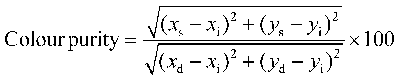
PeLEDs were characterised through a calibrated integrated sphere with barium sulphate coating from Newport. A 2400 Keithley power source supplied the applied bias. The EL spectra were recorded through an Ocean Optics spectrometer (USB2000) coupled to the optical fibre (QP400-2-UV-Vis), and the radiant flux was collected by a silicon photodiode (Hamamatsu S2281-01). In addition, a 6514 Keithley electrometer registered the generated photocurrent. Both the detectors were residing on the wall of the integrated sphere at about 90° from the light source. The colorimetric characteristics were calculated through a designed Python program when feeding our EL spectra. Briefly, the colour coordinates were calculated by solving the integrals of the colour matching functions by discrete numerical sums. From the colour coordinates, the dominant wavelength was determined in the CIE chromaticity diagram by the intersection between the locus curve and the line passing through the white point (illuminant E) and the sample point. Finally, the colour purity was calculated using the expression:where xs,ys are the colour coordinates of the sample, xi,yi those of the white point and xd,yd those of the dominant wavelength.
Conflicts of interest
The authors declare no conflict of interest.Acknowledgements
We thank Arjen Kamp and Teo Zaharia for all the technical support in the laboratory. The University of Groningen is acknowledged for the UNAM scholarship program. Special thanks to B. Juárez García and E. A. González Villa for providing the Python script for the colorimetry analysis. S. K. acknowledge the Deutsche Forschungsgemeinschaft (DFG) for a postdoctoral research fellowship (grant number 408012143). A. M. acknowledge access to research infrastructure in CeSAR – Centro Servizi di Ateneo per la Ricerca- at Universita degli Studi di Cagliari and thank Dr M. Marceddu for technical assistance. This research work received partial financial support from the project PAPIIT-UNAM (number IN111022).References
- M. Lu, Y. Zhang, S. Wang, J. Guo, W. W. Yu and A. L. Rogach, Adv. Funct. Mater., 2019, 29, 1902008 CrossRef.
- L. Protesescu, S. Yakunin, M. I. Bodnarchuk, F. Krieg, R. Caputo, C. H. Hendon, R. X. Yang, A. Walsh and M. V. Kovalenko, Nano Lett., 2015, 15, 3692–3696 CrossRef CAS PubMed.
- Y. Hassan, O. J. Ashton, J. H. Park, G. Li, N. Sakai, B. Wenger, A. A. Haghighirad, N. K. Noel, M. H. Song, B. R. Lee, R. H. Friend and H. J. Snaith, J. Am. Chem. Soc., 2019, 141, 1269–1279 CrossRef CAS PubMed.
- J. H. Heo, J. K. Park and S. H. Im, Cell Rep. Phys. Sci., 2020, 1, 100177 CrossRef.
- Y. H. Kim, S. Kim, A. Kakekhani, J. Park, J. Park, Y. H. Lee, H. Xu, S. Nagane, R. B. Wexler, D. H. Kim, S. H. Jo, L. Martínez-Sarti, P. Tan, A. Sadhanala, G. S. Park, Y. W. Kim, B. Hu, H. J. Bolink, S. Yoo, R. H. Friend, A. M. Rappe and T. W. Lee, Nat. Photonics, 2021, 15, 148–155 CrossRef CAS.
- D. Ma, K. Lin, Y. Dong, H. Choubisa, A. H. Proppe, D. Wu, Y. K. Wang, B. Chen, P. Li, J. Z. Fan, F. Yuan, A. Johnston, Y. Liu, Y. Kang, Z.-H. Lu, Z. Wei and E. H. Sargent, Nature, 2021, 599, 594–598 CrossRef CAS PubMed.
- J. S. Kim, J.-M. Heo, G.-S. Park, S.-J. Woo, C. Cho, H. J. Yun, D.-H. Kim, J. Park, S.-C. Lee, S.-H. Park, E. Yoon, N. C. Greenham and T.-W. Lee, Nature, 2022, 611, 688–694 CrossRef CAS PubMed.
- Y. K. Wang, F. Yuan, Y. Dong, J. Y. Li, A. Johnston, B. Chen, M. I. Saidaminov, C. Zhou, X. Zheng, Y. Hou, K. Bertens, H. Ebe, D. Ma, Z. Deng, S. Yuan, R. Chen, L. K. Sagar, J. Liu, J. Fan, P. Li, X. Li, Y. Gao, M. K. Fung, Z. H. Lu, O. M. Bakr, L. S. Liao and E. H. Sargent, Angew. Chem., Int. Ed., 2021, 60, 16164–16170 CrossRef CAS.
- J. Jiang, Z. Chu, Z. Yin, J. Li, Y. Yang, J. Chen, J. Wu, J. You and X. Zhang, Adv. Mater., 2022, 34, 2204460 CrossRef CAS PubMed.
- Y. Cao, N. Wang, H. Tian, J. Guo, Y. Wei, H. Chen, Y. Miao, W. Zou, K. Pan, Y. He, H. Cao, Y. Ke, M. Xu, Y. Wang, M. Yang, K. Du, Z. Fu, D. Kong, D. Dai, Y. Jin, G. Li, H. Li, Q. Peng, J. Wang and W. Huang, Nature, 2018, 562, 249–253 CrossRef CAS PubMed.
- W. Xu, Q. Hu, S. Bai, C. Bao, Y. Miao, Z. Yuan, T. Borzda, A. J. Barker, E. Tyukalova, Z. Hu, M. Kawecki, H. Wang, Z. Yan, X. Liu, X. Shi, K. Uvdal, M. Fahlman, W. Zhang, M. Duchamp, J. M. Liu, A. Petrozza, J. Wang, L. M. Liu, W. Huang and F. Gao, Nat. Photonics, 2019, 13, 418–424 CrossRef CAS.
- Y. Tian, X. Y. Qian, C. C. Qin, M. H. Cui, Y. Q. Li, Y. C. Ye, J. K. Wang, W. J. Wang and J. X. Tang, Chem. Eng. J., 2021, 415, 129088 CrossRef CAS.
- Q. Wang, X. Wang, Z. Yang, N. Zhou, Y. Deng, J. Zhao, X. Xiao, P. Rudd, A. Moran, Y. Yan and J. Huang, Nat. Commun., 2019, 10, 5633 CrossRef CAS PubMed.
- Z. Chu, Y. Zhao, F. Ma, C. X. Zhang, H. Deng, F. Gao, Q. Ye, J. Meng, Z. Yin, X. Zhang and J. You, Nat. Commun., 2020, 11, 4165 CrossRef CAS PubMed.
- M. Karlsson, Z. Yi, S. Reichert, X. Luo, W. Lin, Z. Zhang, C. Bao, R. Zhang, S. Bai, G. Zheng, P. Teng, L. Duan, Y. Lu, K. Zheng, T. Pullerits, C. Deibel, W. Xu, R. Friend and F. Gao, Nat. Commun., 2021, 12, 361 CrossRef CAS PubMed.
- C. Bi, Z. Yao, J. Hu, X. Wang, M. Zhang, S. Tian, A. Liu, Y. Lu, N. H. de Leeuw, M. Sui and J. Tian, ACS Energy Lett., 2023, 8, 731–739 CrossRef CAS.
- B. Liu, J. Li, G. Wang, F. Ye, H. Yan, M. Zhang, S. C. Dong, L. Lu, P. Huang, T. He, P. Xu, H. S. Kwok and G. Li, Sci. Adv., 2022, 8, eabq0138 CrossRef CAS PubMed.
- Y. Liu, J. Cui, K. Du, H. Tian, Z. He, Q. Zhou, Z. Yang, Y. Deng, D. Chen, X. Zuo, Y. Ren, L. Wang, H. Zhu, B. Zhao, D. Di, J. Wang, R. H. Friend and Y. Jin, Nat. Photonics, 2019, 13, 760–764 CrossRef CAS.
- Y. Yang, S. Xu, Z. Ni, C. H. Van Brackle, L. Zhao, X. Xiao, X. Dai, J. Huang, Y. Yang, S. Xu, Z. Ni, C. H. Van Brackle, L. Zhao, X. Xiao, X. Dai and J. Huang, Adv. Mater., 2021, 33, 2100783 CrossRef CAS PubMed.
- Y. Dong, Y. K. Wang, F. Yuan, A. Johnston, Y. Liu, D. Ma, M. J. Choi, B. Chen, M. Chekini, S. W. Baek, L. K. Sagar, J. Fan, Y. Hou, M. Wu, S. Lee, B. Sun, S. Hoogland, R. Quintero-Bermudez, H. Ebe, P. Todorovic, F. Dinic, P. Li, H. T. Kung, M. I. Saidaminov, E. Kumacheva, E. Spiecker, L. S. Liao, O. Voznyy, Z. H. Lu and E. H. Sargent, Nat. Nanotechnol., 2020, 15, 668–674 CrossRef CAS PubMed.
- S. Liu, Z. Guo, X. Wu, X. Liu, Z. Huang, L. Li, J. Zhang, H. Zhou, L. D. Sun and C. H. Yan, Adv. Mater., 2022, 35, 2208078 CrossRef.
- X. Peng, B. He, H. Zheng, Z. Su, X. Li, L. Ji, T. Zhang, L. Chen, C. Qin, X. Gao, S. Li and X. Yang, ACS Energy Lett., 2023, 8, 339–346 CrossRef CAS.
- A. Liu, C. Bi and J. Tian, Adv. Funct. Mater., 2022, 32, 2207069 CrossRef CAS.
- W. Cai, M. U. Ali, P. Liu, M. He, C. Zhao, Z. Chen, Y. Zang, M. C. Tang, H. Meng, H. Fu, G. Wei and H. L. Yip, Adv. Sci., 2022, 9, 2200393 CrossRef CAS PubMed.
- Y. Tong, X. Bi, S. Xu, H. Min, L. Cheng, Z. Kuang, L. Yuan, F. Zhou, Y. Chu, L. Xu, L. Zhu, N. Zhao, N. Wang, W. Huang and J. Wang, Adv. Mater., 2023, 35, 2207111 CrossRef CAS.
- Y. Jiang, C. Sun, J. Xu, S. Li, M. Cui, X. Fu, Y. Liu, Y. Liu, H. Wan, K. Wei, T. Zhou, W. Zhang, Y. Yang, J. Yang, C. Qin, S. Gao, J. Pan, Y. Liu, S. Hoogland, E. H. Sargent, J. Chen and M. Yuan, Nature, 2022, 612, 679–684 CrossRef CAS PubMed.
- F. Fries and S. Reineke, Sci. Rep., 2019, 9, 15638 CrossRef PubMed.
- S. Chu, Y. Zhang, P. Xiao, W. Chen, R. Tang, Y. Shao, T. Chen, X. Zhang, F. Liu and Z. Xiao, Adv. Mater., 2022, 34, 2108939 CrossRef CAS PubMed.
- Y. Shen, Y. Q. Li, K. Zhang, L. J. Zhang, F. M. Xie, L. Chen, X. Y. Cai, Y. Lu, H. Ren, X. Gao, H. Xie, H. Mao, S. Kera and J. X. Tang, Adv. Funct. Mater., 2022, 32, 2206574 CrossRef CAS.
- Y. Xia, Y. H. Lou, Y. H. Zhou, Y. R. Shi, K. L. Wang, L. Cai, C. H. Chen, F. Hu, Z. K. Wang and L. S. Liao, Adv. Funct. Mater., 2022, 32, 2208538 CrossRef CAS.
- H. Zhu, G. Tong, J. Li, E. Xu, X. Tao, Y. Sheng, J. Tang and Y. Jiang, Adv. Mater., 2022, 34, 2205092 CrossRef CAS PubMed.
- S. Gonzalez-Carrero, L. Francés-Soriano, M. González-Béjar, S. Agouram, R. E. Galian and J. Pérez-Prieto, Small, 2016, 12, 5245–5250 CrossRef CAS PubMed.
- M. P. Hautzinger, D. Pan, A. K. Pigg, Y. Fu, D. J. Morrow, M. Leng, M. Y. Kuo, N. Spitha, D. P. Lafayette, D. D. Kohler, J. C. Wright and S. Jin, ACS Energy Lett., 2020, 5, 1430–1437 CrossRef CAS.
- J. Cui, Y. Liu, Y. Deng, C. Lin, Z. Fang, C. Xiang, P. Bai, K. Du, X. Zuo, K. Wen, S. Gong, H. He, Z. Ye, Y. Gao, H. Tian, B. Zhao, J. Wang and Y. Jin, Sci. Adv., 2021, 7, eabg8458 CrossRef CAS PubMed.
- X. Xiao, Y. Li and R. J. Xie, Nanoscale, 2020, 12, 9231–9239 RSC.
- S. Shao, H. Duim, Q. Wang, B. Xu, J. Dong, S. Adjokatse, G. R. Blake, L. Protesescu, G. Portale, J. Hou, M. Saba and M. A. Loi, ACS Energy Lett., 2020, 5, 39–46 CrossRef CAS.
- M. Righetto, D. Giovanni, S. S. Lim and T. C. Sum, Appl. Phys. Rev., 2021, 8, 011318 CAS.
- Y. Liu, L. Zhang, S. Chen, C. Liu, Y. Li, J. Wu, D. Wang, Z. Jiang, Y. Li, Y. Li, X. Wang and B. Xu, Small, 2021, 17, 2101477 CrossRef CAS PubMed.
- X. Wang, L. Cai, Y. Zou, D. Liang, L. Wang, Y. Li, J. Zang, G. Bai, X. Gao, T. Song and B. Sun, Nanoscale, 2021, 13, 13497–13505 RSC.
- Y. Liu, L. K. Ono, G. Tong, H. Zhang and Y. Qi, ACS Energy Lett., 2021, 6, 908–914 CrossRef CAS.
- Y. Lian, Y. Yang, L. He, X. Yang, J. Gao, C. Qin, L. Niu and X. Yang, ACS Appl. Mater. Interfaces, 2022, 14, 1659–1669 CrossRef CAS PubMed.
- C. Qin, L. Xu, Z. Zhou, J. Song, S. Ma, Z. Jiao and Y. Jiang, J. Mater. Chem. A, 2022, 10, 3069–3076 RSC.
- R. Quintero-Bermudez, A. Gold-Parker, A. H. Proppe, R. Munir, Z. Yang, S. O. Kelley, A. Amassian, M. F. Toney and E. H. Sargent, Nat. Mater., 2018, 17, 900–907 CrossRef CAS PubMed.
- Y. Han, S. Park, J. Wang, S. Jariwala, K. Lee, C. G. Bischak, S. Kim, J. Hong, S. Kim, M. J. Lee, D. S. Ginger and I. Hwang, Adv. Mater. Interfaces, 2020, 7, 1901860 CrossRef CAS.
- Y. Xia, Y. H. Lou, Y. H. Zhou, K. L. Wang, J. Chen, Z. K. Wang and L. S. Liao, J. Mater. Chem. C, 2022, 10, 3276–3286 RSC.
- S. Yudco, A. S. Dayan, B. El Cohen, T. Binyamin and L. Etgar, J. Mater. Chem. C, 2022, 10, 10037–10046 RSC.
- C. Sun, Y. Jiang, M. Cui, L. Qiao, J. Wei, Y. Huang, L. Zhang, T. He, S. Li, H. Y. Hsu, C. Qin, R. Long and M. Yuan, Nat. Commun., 2021, 12, 2207 CrossRef CAS PubMed.
- F. Zhang, H. Lu, J. Tong, J. J. Berry, M. C. Beard and K. Zhu, Energy Environ. Sci., 2020, 13, 1154–1186 RSC.
- J. Yao, H. Wang, P. Wang, R. S. Gurney, A. Intaniwet, P. Ruankham, S. Choopun, D. Liu and T. Wang, Mater. Chem. Front., 2019, 3, 1357–1364 RSC.
- Y. Zhao, P. Zhu, S. Huang, S. Tan, M. Wang, R. Wang, J. Xue, T. H. Han, S. J. Lee, A. Zhang, T. Huang, P. Cheng, D. Meng, J. W. Lee, J. Marian, J. Zhu and Y. Yang, J. Am. Chem. Soc., 2020, 142, 20071–20079 CrossRef CAS PubMed.
- S. Liu, Y. Guan, Y. Sheng, Y. Hu, Y. Rong, A. Mei and H. Han, Adv. Energy Mater., 2020, 10, 1902492 CrossRef CAS.
- C. Xu, Z. Zhang, S. Zhang, H. Si, S. Ma, W. Fan, Z. Xiong, Q. Liao, A. Sattar, Z. Kang and Y. Zhang, Adv. Funct. Mater., 2021, 31, 2009425 CrossRef CAS.
- Z. Liu, W. Qiu, X. Peng, G. Sun, X. Liu, D. Liu, Z. Li, F. He, C. Shen, Q. Gu, F. Ma, H. L. Yip, L. Hou, Z. Qi and S. J. Su, Adv. Mater., 2021, 33, 2103268 CrossRef CAS PubMed.
- M. Long, T. Zhang, D. Chen, M. Qin, Z. Chen, L. Gong, X. Lu, F. Xie, W. Xie, J. Chen and J. Xu, ACS Energy Lett., 2019, 4, 1025–1033 CrossRef CAS.
- T. L. Leung, H. W. Tam, F. Liu, J. Lin, A. M. C. Ng, W. K. Chan, W. Chen, Z. He, I. Lončarić, L. Grisanti, C. Ma, K. S. Wong, Y. S. Lau, F. Zhu, Ž. Skoko, J. Popović and A. B. Djurišić, Adv. Opt. Mater., 2020, 8, 1901679 CrossRef CAS.
- J. Xing, Y. Zhao, M. Askerka, L. N. Quan, X. Gong, W. Zhao, J. Zhao, H. Tan, G. Long, L. Gao, Z. Yang, O. Voznyy, J. Tang, Z. H. Lu, Q. Xiong and E. H. Sargent, Nat. Commun., 2018, 9, 3541 CrossRef PubMed.
- Y. Chen, Y. Sun, J. Peng, W. Zhang, X. Su, K. Zheng, T. Pullerits and Z. Liang, Adv. Energy Mater., 2017, 7, 1700162 CrossRef.
- Q. Wang, S. Shao, B. Xu, H. Duim, J. Dong, S. Adjokatse, G. Portale, J. Hou, M. Saba and M. A. Loi, ACS Appl. Mater. Interfaces, 2020, 12, 29505–29512 CAS.
- L. N. Quan, Y. Zhao, F. Pelayo García De Arquer, R. Sabatini, G. Walters, O. Voznyy, R. Comin, Y. Li, J. Z. Fan, H. Tan, J. Pan, M. Yuan, O. M. Bakr, Z. Lu, D. H. Kim and E. H. Sargent, Nano Lett., 2017, 17, 3701–3709 CrossRef CAS PubMed.
- L. Zhang, C. Sun, T. He, Y. Jiang, J. Wei, Y. Huang and M. Yuan, Light: Sci. Appl., 2021, 10, 61 CrossRef CAS PubMed.
- M. Yuan, L. N. Quan, R. Comin, G. Walters, R. Sabatini, O. Voznyy, S. Hoogland, Y. Zhao, E. M. Beauregard, P. Kanjanaboos, Z. Lu, D. H. Kim and E. H. Sargent, Nat. Nanotechnol., 2016, 11, 872–877 CrossRef CAS PubMed.
- L. Lei, D. Seyitliyev, S. Stuard, J. Mendes, Q. Dong, X. Fu, Y. Chen, S. He, X. Yi, L. Zhu, C. Chang, H. Ade, K. Gundogdu and F. So, Adv. Mater., 2020, 32, 1906571 CrossRef CAS PubMed.
- Q. Wang, S. Shao, B. Xu, H. Duim, J. Dong, S. Adjokatse, G. Portale, J. Hou, M. Saba and M. A. Loi, ACS Appl. Mater. Interfaces, 2020, 12, 45 Search PubMed.
- J. Dong, S. Shao, S. Kahmann, A. J. Rommens, D. Hermida-Merino, G. H. ten Brink, M. A. Loi and G. Portale, Adv. Funct. Mater., 2020, 30, 2001294 CrossRef CAS.
- K. Shibuya, M. Koshimizu, F. Nishikido, H. Saito and S. Kishimoto, Acta Crystallogr., Sect. E: Struct. Rep. Online, 2009, 65, m1323–m1324 CrossRef CAS PubMed.
- Y. Liao, H. Liu, W. Zhou, D. Yang, Y. Shang, Z. Shi, B. Li, X. Jiang, L. Zhang, L. N. Quan, R. Quintero-Bermudez, B. R. Sutherland, Q. Mi, E. H. Sargent and Z. Ning, J. Am. Chem. Soc., 2017, 139, 6693–6699 CrossRef CAS PubMed.
- H. Lee, H. Kim, H. Cho, W. Cha, Y. Hong, Y. Kim, A. Sadhanala, V. Venugopalan, J. S. Kim, J. W. Choi, C. Lee, D. Kim, H. Yang, R. H. Friend and T. Lee, Adv. Funct. Mater., 2019, 29, 1901225 CrossRef.
- D. B. Kim, S. Lee, C. H. Jang, J. H. Park, A. Lee and M. H. Song, Adv. Mater. Interfaces, 2020, 7, 1902158 CrossRef CAS.
- M. J. Rivera-Medina, A. Carrillo-Verduzco, A. Rodríguez-Gómez, M. A. Loi and J. C. Alonso-Huitrón, Mater. Chem. Phys., 2021, 270, 124866 CrossRef CAS.
- X. Yang, X. Xu and G. Zhou, J. Mater. Chem. C, 2015, 3, 913–944 RSC.
- S. Shao, J. Liu, G. Portale, H.-H. Fang, G. R. Blake, G. H. ten Brink, L. J. A. Koster and M. A. Loi, Adv. Energy Mater., 2018, 8, 1702019 CrossRef.
Footnotes |
| † Electronic supplementary information (ESI) available. See DOI: https://doi.org/10.1039/d3nr00087g |
| ‡ New address: Cavendish Laboratory, University of Cambridge, University of Cambridge, JJ Thomson Avenue CB30HE, Cambridge, UK. |
| § New address: Key Laboratory for Physical Electronics and Devices of the Ministry of Education & Shaanxii Key Lab of Information Photonic Technique, School of Electronic Science and Engineering, Xi'an Jiaotong University, Xi'an, 710049, China. |
| This journal is © The Royal Society of Chemistry 2023 |