
Highly stable, substrate-free, and flexible broadband halide perovskite paper photodetectors†
Lam-Gia-Hao
Dao
,
Chih-Hao
Chiang
,
Sumedh M.
Shirsat
,
Thi-Quynh-Hoa
Nguyen
,
Jitendra
Singh
,
Han-Song
Wu
,
Yu-Lun
Liu
and
Meng-Lin
Tsai
 *
*
Department of Materials Science and Engineering, National Taiwan University of Science and Technology, Taipei 106335, Taiwan. E-mail: mltsai@mail.ntust.edu.tw
First published on 14th March 2023
Abstract
In this work, we aim to fabricate a highly stable and flexible perovskite paper photodetector based on a Zn-doped MA0.6FA0.4PbI3 perovskite and CNC. The paper photodetector has been successfully synthesized by the vacuum filtration method and deposited with interdigitated electrodes. The paper photodetector exhibits a significant photoresponse with a responsivity of 0.23 A W−1 under 650 nm light irradiation when operated at 5 V. The stability of the paper photodetector has also been tested and it shows high photoresponse after 30 days under ambient conditions. Therefore, this paper photodetector holds promise for developing efficient, stable, and flexible optoelectronic devices in the future.
Introduction
Halide perovskites have attracted extensive attention in recent years due to their outstanding properties in the development of various optoelectronic devices including photodetectors, solar cells, light-emitting diodes (LEDs), and field effect transistors (FETs).1–4 Despite their great performance in terms of a wide absorption range, narrow emission width, high wavelength tunability, ultrahigh quantum yield, and hysteresis-free behavior, the stability problem has remained a major challenge for their practical application.5–7 Halide perovskite materials suffer from various instability problems including structural, interfacial, and environmental instabilities. Recently, many studies have been carried out to improve the interface stability of perovskite light emitting/conversion or photodetection devices through various passivation methods. For perovskite nanocrystal-based light emitting devices, conventionally used capping ligands such as oleic acid and oleylamine exhibit a dynamic nature which makes them highly sensitive to moisture. Therefore, strategies such as phthalimide passivation, benzoic acid treatment, and ascorbic acid post-treatment have been applied to increase the stability as well as the quantum yield of perovskite nanocrystals.8–14 For photodetection devices, small organic molecules such as sec-pentanol have been used as polar additives to improve the crystallization of the perovskite films and reduce the grain boundaries.15 A fluorous polymer has also been used on the perovskite film as a light protective layer.16 Ye et al. used the amino groups of 1H,1H-perfluorooctylamine (PFA) to bind with the Pb2+ of perovskite microwires. The hydrophobic fluorocarbon alkyl chains in PFA can prevent the perovskite microwires from moisture. The PFA-modified device retained 80% of its initial performance after 30 days under ambient conditions.17 Ma et al. mixed poly[48-bis(5-(2-ethylhexyl)thiophen-2-yl)benzo[1,2-b;4,5-b′]dithiophene-2,6-diyl-alt-(4-(2-ethylhexyl)-3-fluorothieno[3,4-b]thiophene-2-carboxylate-2-6-diyl)] (PCE10) and polystyrene (PS) with the precursor solution. These polymers with a large dipole moment can suppress the ion migration of the device, resulting in stability enhancement.18Paper is a flexible material that is light weight, biodegradable, and recyclable. Recently, various paper electronics including transistors, diodes, photodetectors, memory devices, photovoltaics, and even batteries have been developed.19–24 Therefore, with the development of paper electronics, the properties and processing of cellulose materials play important roles in the mechanical properties and electrical properties, as well as the biodegradability and environmental compatibility of the devices. Among various cellulose based materials, cellulose nanocrystals (CNCs) have been reported to exhibit a large surface area, a high aspect ratio, high mechanical strength, and adjustable surface chemistry.25,26 In addition, CNCs can be obtained through the acid hydrolysis of cellulose to form hybrids with other nanomaterials including nanocrystals, nanowires, and nanoplatelets. Previously, we have shown that CNC surface-passivated halide perovskites possess better stability and optical characteristics. The organosulfate groups on CNCs with high electronegativity can attach to the exposed Pb ions of halide perovskite nanocrystals and reduce the trapping states caused by halide vacancies.27
In the development of flexible devices, most of the flexible optoelectronic devices are fabricated simply using flexible substrates such as polyimide (PI), polyethylene terephthalate (PET), polymethyl methacrylate (PMMA), or papers with electrodes, transport layers, and active layers on top of them.1,28 Therefore, additional packaging techniques should be applied to further protect the device from degradation. By adopting substrate-free fabrication techniques, electronic circuits and devices can be fully embedded within the matrix for further reducing the manufacturing waste, cost, and weight of the device. These properties are in high demand in applications such as e-skin and wearable electronics.29 Recently, CNCs with controllable conductivity have been achieved by performing functionalization techniques to form functional groups.25,26 Moreover, hydrophilic and hydrophobic properties can also be adjusted through various functionalization techniques. Apart from the encapsulation of electronic devices, it is expected that CNCs can play an important role in improving the interface stability.
In our perivous study, we have shown that the performance of CsPbI3 perovskite quantum dots can be efficiently enhanced by doping Zn due to the improved structural stability of iodide-based perovskites.30 Moreover, excess ZnI2 can form an iodide-rich condition during paper fabrication to facilitate the formation of perovskite crystals. Herein, we combine the advantage of CNCs and Zn dopants to synthesize highly stable Zn-doped MA0.6FA0.4PbI3/CNC papers. The technique can be applied to fabricate substrate-free and flexible photodetectors by directly depositing a metal electrode on the as-synthesized perovskite paper. The paper photodetector exhibits a significant photoresponse with a responsivity of 0.23 A W−1 under 650 nm laser irradiation when operated at 5 V. The photoresponse retains 65% of its original value after 30 days under ambient conditions. In addition, the responsivity of the paper photodetector retains ∼80% of its original value after 3000 bending cycles. Due to its high stability and flexibility, the perovskite paper photodetector shows great potential for long-term operation of photodetector devices.
Results and discussion
Fig. 1a shows the structure of the Zn-doped MA0.6FA0.4PbI3/CNC paper. The presence of organosulfate groups with high electronegativity on CNCs (–OSO3−) can provide a strong binding strength to the exposed Pb on the surface of perovskite crystals and stabilize the structure of perovskites to achieve surface passivation. In addition, the long carbon chains and hydrogen bonds between CNCs can also prevent perovskites from oxygen and moisture-induced degradation. The photographic images of the bare CNC paper and the Zn-doped MA0.6FA0.4PbI3/CNC paper are shown in Fig. 1b. The bare CNC paper is highly transparent and the Zn-doped MA0.6FA0.4PbI3/CNC paper is extremely dark, showing great potential in light absorption. Fig. 1c shows the schematic of the fabrication process of the paper photodetector. The details of the experimental procedure are further explained in the Experimental section. The absorbance spectra and of the bare CNC paper, the Zn-doped MAPbI3/CNC paper, and the Zn-doped MA0.6FA0.4PbI3/CNC paper are shown in Fig. 2a. It can be observed that the absorbance of the Zn-doped MA0.6FA0.4PbI3/CNC paper exhibits a wider absorption wavelength range than those without FA+, indicating its broadband absorption behavior. The fluorescence spectra of Zn-doped MA0.6FA0.4PbI3/CNC and Zn-doped MAPbI3/CNC papers are also shown in Fig. 2a (dashed line). The emission peaks of Zn-doped MA0.6FA0.4PbI3/CNC and Zn-doped MAPbI3/CNC papers are around 809 nm and 762 nm, respectively. The optical band gap was determined using the Tauc plot (Fig. 2b) and the calculated value is around 1.49 eV. The X-ray diffraction (XRD) patterns of the bare CNC paper, Zn-doped MA0.6FA0.4PbI3/CNC paper, and Zn-doped MA0.6FA0.4PbI3 paper are shown in Fig. 2c. The diffraction peaks of the bare CNC paper at 15° and 22° correspond to the (110) and (200) planes of CNCs, respectively.27,30 The diffraction peaks of the Zn-doped MA0.6FA0.4PbI3/CNC paper are 15°, 21°, 25°, 28.4°, 31.8°, 35°, 40.5°, and 43°, which correspond to the (110), (112), (211), (220), (310), (312), (224), and (330) planes of the Zn-doped MA0.6FA0.4PbI3 perovskite. However, the (110) and (211) peaks of the Zn-doped MA0.6FA0.4PbI3/CNC paper overlap with the (110) and (200) peaks of CNC due to the broader peak width of CNC.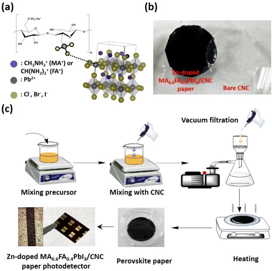 | ||
| Fig. 1 (a) Schematic of a Zn-doped MA0.6FA0.4PbI3/CNC structure. (b) Photographic images of bare CNC and Zn-doped MA0.6FA0.4PbI3/CNC papers. (c) Experimental procedure and photograph of the paper photodetector. | ||
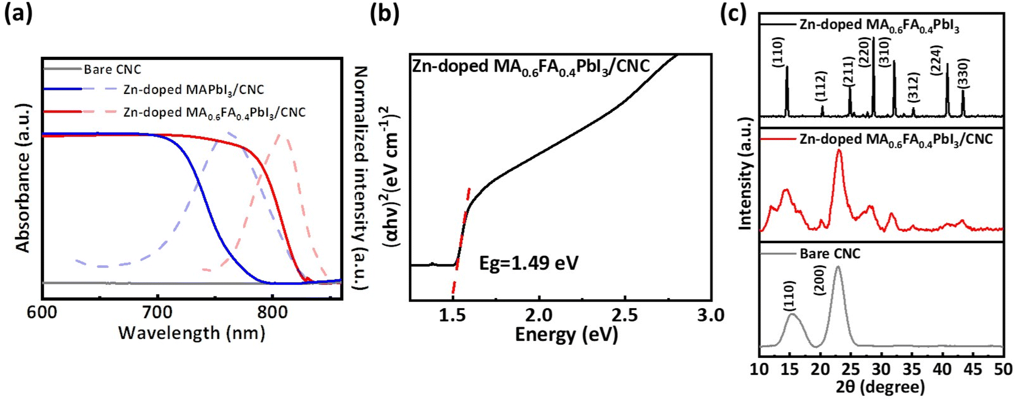 | ||
| Fig. 2 (a) Absorbance spectra of bare CNC, Zn-doped MA0.6FA0.4PbI3/CNC, and Zn-doped MAPbI3/CNC papers and fluorescence spectra of Zn-doped MA0.6FA0.4PbI3/CNC and Zn-doped MAPbI3/CNC papers (dashed lines). (b) Tauc plot of the Zn-doped MA0.6FA0.4PbI3/CNC paper. (c) XRD patterns of bare CNC, Zn-doped MA0.6FA0.4PbI3/CNC papers, and Zn-doped MA0.6FA0.4PbI3 films. | ||
The scanning electron microscopic (SEM) images of the Zn-doped MA0.6FA0.4PbI3/CNC paper and Zn-doped MA0.6FA0.4PbI3 films are shown in Fig. 3a and b, respectively. The size of perovskite crystals in the Zn-doped MA0.6FA0.4PbI3 films is around 2–8 μm. On the other hand, the size of perovskite crystals in the Zn-doped MA0.6FA0.4PbI3/CNC paper is <1 μm due to the growth limited by CNC. The transmission electron microscopy (TEM), high resolution transmission electron microscopy (HRTEM), and fast Fourier transform (FFT) images of the Zn-doped MA0.6FA0.4PbI3/CNC paper and Zn-doped MA0.6FA0.4PbI3 are shown in Fig. S2.† The d-spacing of (220) in the Zn-doped MA0.6FA0.4PbI3/CNC paper has been found to be around 0.32 nm, which is consistent with that obtained in Zn-doped MA0.6FA0.4PbI3 without CNC (0.318 nm).
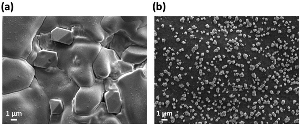 | ||
| Fig. 3 (a) SEM image of the Zn-doped MA0.6FA0.4PbI3 film. (b) SEM image of the Zn-doped MA0.6FA0.4PbI3/CNC paper. | ||
For device fabrication, 5 nm/95 nm of Ti/Au was deposited on the paper through electron-beam evaporation with interdigitated electrode patterns defined by a shadow mask. The photographs of the paper before and after electron-beam evaporation are shown in Fig. S1a.† It can be observed that the appearance of the paper does not obviously change after the evaporation process. Moreover, the XRD patterns of the paper before and after electron beam evaporation were collected and are shown in Fig. S1b.† The diffraction peaks of the paper show similar patterns before and after the evaporation, indicating that the structure of the perovskite crystals does not change after the evaporation process.
Fig. 4a, b, and c show the characteristic curves of the paper photodetector under 450 nm, 520 nm, and 650 nm laser light irradiation, respectively. It can be observed that the current increases with increasing power density of the excitation laser. Fig. 4d, e, and f show the photoresponsivity as a function of power density and bias voltages (operated from 3 V to 5 V) under 450 nm, 520 nm, and 650 nm laser light irradiation, respectively. It can be observed that responsivity decreases rapidly with increasing power density due to the decreasing empty states in the conduction band. The highest photoresponse of 0.23 A W−1 (with 650 nm laser irradiation) can be observed under a power density of 0.3 mW cm−2 at an applied bias voltage of 5 V. As shown in Fig. 5a, the current–time (I–t) curves of the paper photodetector were obtained from 1 V to 5 V at an interval of 1 V under 650 nm (35 mW cm−2) laser irradiation. Based on the results, the device exhibits good photocurrent stability, fast response, and consistent response in numerous ON–OFF cycles. Additionally, the paper photodetector exhibits a fast temporal photoresponse. The rise and fall time are 600 μs and 709 μs, respectively (Fig. 5b).
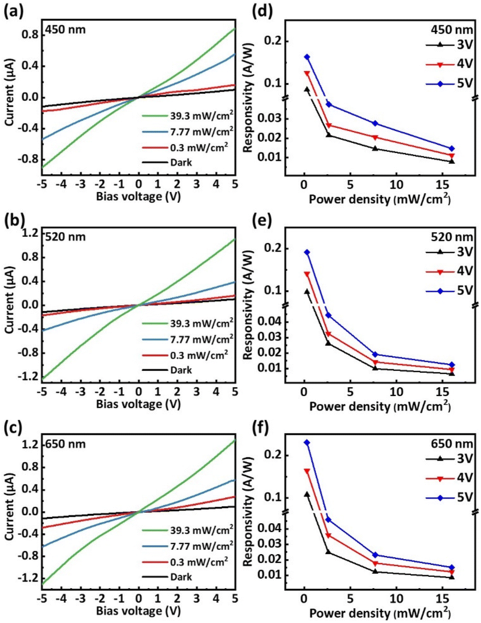 | ||
| Fig. 4 I–V curves of the paper photodetector under dark and light illumination conditions at (a) 450 nm, (b) 520 nm, and (c) 650 nm laser irradiation. Power density dependent responsivity of the paper photodetector under (d) 450 nm, (e) 520 nm, and (f) 650 nm laser irradiation. | ||
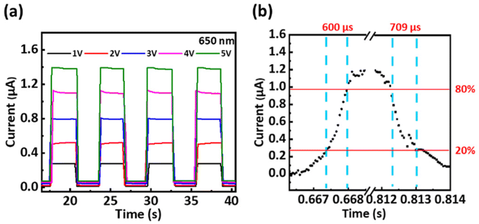 | ||
| Fig. 5 (a) Time response at various applied voltages under 650 nm laser irradiation. (b) I–t curve of the paper photodetector in a cycle. | ||
In order to demonstrate the flexibility of the paper photodetector, bending test has been carried out and the schematic is shown in Fig. 6a. The paper photodetector is bended from flat to curved (angle of bend = 180°) and then back to flat as a bending cycle. The result of the bending test was recorded and is shown in Fig. 6b. The relative responsivity is defined as the responsivity divided by the initial responsivity. The responsivity of the paper photodetector remains at 94%, 87%, and ∼70% of the original value after 500, 1000, and 3000 bending cycles, respectively. The curve shows a linear degradation after each bending cycle. Fig. 6c shows the stability test results of the bare Zn-doped MA0.6FA0.4PbI3 film on a SiO2/Si substrate and the paper photodetector. The responsivity of the paper photodetector retained 65% of its original value after 30 days under ambient conditions (temperature of 25 °C and relative humidity of 70%), whereas the bare Zn-doped MA0.6FA0.4PbI3 film on the substrate quickly degrades to 0% in only 3 days. Moreover, doping Zn into iodide-based perovskites can further enhance the stability. Fig. S3a and S3b† show the photographs of the Zn-doped MA0.6FA0.4PbI3 film and the MA0.6FA0.4PbI3 film under ambient conditions immediately after drop-coating (0 h) and after 20 h. The color of the undoped MA0.6FA0.4PbI3 film has changed after 20 h due to degradation. Therefore, the enhanced stability of the paper photodetector can be attributed to the combination of the long carbon chain of CNC, the strong binding strength between the organosulfate (–OSO3−) groups of CNC, and Zn dopants within the perovskite structure.
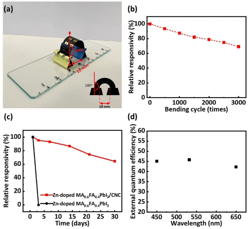 | ||
| Fig. 6 (a) Schematic of the bending test of the paper photodetector. (b) Stability of the paper photodetector after various bending cycles. (c) Stabilities of the paper and bare Zn-doped MA0.6FA0.4PbI3 photodetectors under ambient conditions. (d) EQE of the paper photodetectors under 450 nm, 520 nm, and 650 nm laser irradiation. | ||
Fig. 6d shows the calculated external quantum efficiency (EQE) under 450 nm, 520 nm, and 650 nm laser irradiation using the following equation:
 | (1) |
| Substrate type | Devices | Bias voltage | Response range | R (A W−1) | Bending cycles | Bending condition | Bending stability | Response time | Ref. |
|---|---|---|---|---|---|---|---|---|---|
| PI | Au/MAPbI3/Au | 0 | 300 nm | 0.0022 | — | R = 3.7 mm | — | T r = 27.2, Tf = 26.2 (ms) | 31 |
| PET | Au/MAPbI3/Au | 10 | 650 nm | 0.1 | 10![[thin space (1/6-em)]](https://www.rsc.org/images/entities/char_2009.gif) 000 000 |
θ = 40° | 90% | ∼0.3 ms | 32 |
| PEN | Au/P(VDF-TrFE)/MAPbI3 nanowires/Au | 0 | 650 nm | 0.012 | 100 | θ = 45° | ∼75% | T r = 88, Tf = 154 (μs) | 33 |
| PET | ITO/MAPbI3/Al | 26 | 459 nm | 0.004 | — | R = 5 mm | 66% | T r = 50, Tf = 120 (μs) | 34 |
| PET | Au/PbPc/MAPbI3−xClx/Au | 50 | 655 nm | 0.152 | 1000 | R = 6.5 mm | ∼99% | T r = 632, Tf = 680 (μs) | 35 |
| θ = 80° | |||||||||
| PEN | Au/MAPbI3/RhB/Au | 5 | 550 nm | 0.0426 | 1000 | R = 9 mm | 92.7% | T r = 60, Tf = 40 (ms) | 36 |
| PEN | Au/P(VDF-TrFE)/MAPbI3/Au | 0 | 650 nm | 0.02 | 200 | θ = 120° | ∼90% | T r = 92, Tf = 193 (μs) | 37 |
| Substrate-free | Au + Ti/MAPbI3 + CNC/Ti + Au | 5 | 650 nm | 0.23 | 1000 | R = 2 mm | 87% | T r = 600, Tf = 709 (μs) | This work |
| θ = 180° |
Conclusions
In summary, we have demonstrated the synthesis, characterization, and fabrication of a Zn-doped MA0.6FA0.4PbI3 perovskite paper photodetector. It is shown in the bending test that the paper photodetector retains 70% of its initial responsivity after 3000 bending cycles. In addition, the responsivity of the device retains 65% of its initial value after 30 days under ambient conditions. Moreover, the paper device exhibits a considerable responsivity of up to 0.23 A W−1. As a result, the substrate-free, flexible, stable, broadband, and high responsivity paper photodetector holds the potential for the future development of optoelectronic and photosensing devices.Experimental section
Chemicals
Methylammonium iodide (MAI, FMPV, 99%), formamidinium iodide (FAI, FMPV, 99%), zinc iodide (ZnI2, SHOWA, 98%), lead iodide (PbI2, ACROS, 99%), cellulose nanocrystals (CNC, Celluforce), dimethylformamide (DMF, Echo, 99%), and deionized (DI) water were used.Preparation of the dispersed CNC solution
5 wt% of a CNC/DI water mixture was prepared by dissolving CNC powders in DI water. Then, an appropriate amount of the as-prepared CNC/DI water mixture was dispersed in DMF to prepare 1 wt% of dispersed CNC solution. The solution was kept at room temperature for subsequent procedures.Preparation of the Zn-doped MA0.6FA0.4PbI3 precursor solution
To prepare the Zn-doped MA0.6FA0.4PbI3 precursor solution, 2.4 mmol of MAI, 1.6 mmol of FAI, 4 mmol of PbI2, and 0.4 mmol of ZnI2 were dissolved in 5 mL of DMF. The precursor solution was kept stirred until all the powders were completely dissolved. The precursor solution was then kept at room temperature for subsequent procedures.Preparation of the Zn-doped MAPbI3 precursor solution
To prepare the Zn-doped MAPbI3 solution, 4 mmol of MAI, 4 mmol of PbI2, and 0.4 mmol of ZnI2 were dissolved in 5 mL of DMF. The precursor solution was kept stirred until all the powders were completely dissolved. The precursor solution was then kept at room temperature for subsequent procedures.Preparation of the MA0.6FA0.4PbI3 precursor solution
To prepare the MA0.6FA0.4PbI3 precursor solution, 2.4 mmol of MAI, 1.6 mmol of FAI, and 4 mmol of PbI2 were dissolved in 5 mL of DMF. The precursor solution was kept stirred until all the powders were completely dissolved. The precursor solution was then kept at room temperature for subsequent procedures.Fabrication of the Zn-doped MA0.6FA0.4PbI3 photodetector
1 mL of the Zn-doped MA0.6FA0.4PbI3 precursor was directly dropped on the SiO2/Si substrate and dried on a hot plate at 80 °C overnight. 5 nm/95 nm of Ni/Au was deposited on the paper through electron beam evaporation with interdigitated electrode patterns defined by a shadow mask.Fabrication of the Zn-doped MA0.6FA0.4PbI3/CNC paper photodetector
5 mL of the as-prepared precursor and 5 mL of the as-prepared dispersed CNC solution were mixed and stirred to obtain a homogeneous mixture. Afterwards, the mixture was poured into a Buchner funnel with a 0.02 μm pore size ceramic filter to perform vacuum filtration. This procedure was kept on until all of the remaining solvent was drained for 30 min. Then the paper was dried at 60 °C in an oven for 24 h until the paper can be easily separated from the ceramic filter. For device fabrication, 5 nm/95 nm of Ti/Au was deposited on the paper through electron beam evaporation with interdigitated electrode patterns defined by a shadow mask. The active area of the device is ∼0.27 mm2 defined by the open area between the interdigitated fingers.Characterization
The crystal structures of the papers were measured using a D2 phaser X-ray diffractometer (Bruker). The photoluminescence spectra of the papers were recorded using a spectrofluorometer (JASCO FP8500). The transmittance and absorbance spectra of the papers were recorded using a UV-vis-NIR spectrophotometer (JASCO V670). The characteristic curves of paper photodetector were confirmed using a sourcemeter (Keithley 2612B) with a probestation and power tunable laser light sources (450 nm, 520 nm, and 650 nm). The light powers were measured using a power meter (LP10, SANWA, Japan). The transmission electron microscopy and high-resolution transmission electron microscopy images were collected using an FEI (Thermo Fisher Scientific), Talos F200XG2. The scanning electron microscope images were collected using a JEOL 7900F.Author contributions
L. G. H. D. conceived this study and designed the experiments. L. G. H. D., C. H. C., and M. L. T. wrote the manuscript. L. G. H. D., S. M. S., T. Q. H. N., J. S., H. S. W., and Y. L. L. carried out the experiments. M. L. T. guided the project.Conflicts of interest
There are no conflicts to declare.Acknowledgements
This work was supported by the National Science and Technology Council of Taiwan under project No. 110-2221-E-011-076 and 111-2222-E-011-001.References
- X. Hu, X. Zhang, L. Liang, J. Bao, S. Li, W. Yang and Y. Xie, Adv. Funct. Mater., 2014, 24(46), 7373–7380 CrossRef CAS.
- A. K. Jena, A. Kulkarni and T. Miyasaka, Chem. Rev., 2019, 119(5), 3036–3103 CrossRef CAS PubMed.
- X. K. Liu, W. Xu, S. Bai, Y. Jin, J. Wang, R. H. Friend and F. Gao, Nat. Mater., 2021, 20, 10–21 CrossRef CAS PubMed.
- A. Liu, H. Zhu, S. Bai, Y. Reo, T. Zou, M. G. Kim and Y. Y. Noh, Nat. Electron., 2022, 5, 78–83 CrossRef CAS.
- S. Wang, A. A. Y. Amin, L. Wu, M. Cao, Q. Zhang and T. Ameri, Small Struct., 2021, 2, 2000124 CrossRef CAS.
- D. Wang, M. Wright, N. K. Elumalai and A. Uddin, Sol. Energy Mater. Sol. Cells, 2016, 147, 255–275 CrossRef CAS.
- Y. Wei, Z. Cheng and J. Lin, Chem. Soc. Rev., 2019, 48, 310–350 RSC.
- V. G. V. Dutt, S. Akhil and N. Mishra, Nanoscale, 2021, 13, 14442 RSC.
- V. G. V. Dutt, S. Akhil, R. Singh, M. Palabathuni and N. Mishra, J. Phys. Chem. C, 2022, 126, 9502–9508 CrossRef CAS.
- S. Akhil, V. G. V. Dutt, R. Singh and N. Mishra, J. Phys. Chem. C, 2022, 126, 10742–10751 CrossRef CAS.
- S. Akhil, V. G. V. Dutt and N. Mishra, ChemNanoMat, 2021, 7, 342–353 CrossRef CAS.
- V. G. V. Dutt, S. Akhil, R. Singh, M. Palabathuni and N. Mishra, ACS Appl. Nano Mater., 2022, 5, 5972–5982 CrossRef CAS.
- S. Akhil, V. G. V. Dutt and N. Mishra, Nanoscale, 2021, 13, 13142 RSC.
- V. G. V. Dutt, S. Akhil and N. Mishra, ChemistrySelect, 2021, 6, 8171–8176 CrossRef.
- T. Li, Q. Li, X. Tang, Z. Chen, Y. Li, H. Zhao, S. Wang, X. Ding, Y. Zhang and J. Yao, J. Phys. Chem. C, 2021, 125(5), 2850 CrossRef CAS.
- Y. Guo, C. Liu, H. Tanaka and E. Nakamura, J. Phys. Chem. Lett., 2015, 6(3), 535 CrossRef CAS PubMed.
- Q. Ye, J. Zhang, P. Guo, H. Fan, D. Shchukin, B. Wei and H. Wang, ACS Appl. Mater. Interfaces, 2018, 10(50), 43850 CrossRef CAS PubMed.
- Y. Ma, Y. Cheng, X. Xu, M. Li, C. Zhang, S. H. Cheung, Z. Zeng, D. Shen, Y. M. Xie, K. L. Chiu, F. Lin, S. K. So, C. S. Lee and S. W. Tsang, Adv. Funct. Mater., 2020, 31(3), 2006802 CrossRef.
- R. Martins, D. Gaspar, M. J. Mendes, L. Pereira, J. Martins, P. Bahubalindruni, P. Barquinha and E. Fortunato, Appl. Mater. Today, 2018, 12, 402–414 CrossRef.
- W. Zhang, X. Zhang, C. Lu, Y. Wang and Y. Deng, J. Phys. Chem. C, 2012, 116(16), 9227–9234 CrossRef CAS.
- C. H. Lin, H. C. Fu, B. Cheng, M. L. Tsai, W. Luo, L. Zhou, S. H. Jang, L. Hu and J. H. He, npj 2D Mater. Appl., 2018, 2, 23 CrossRef.
- D. H. Lien, Z. K. Kao, T. H. Huang, Y. C. Liao, S. C. Lee and J. H. He, ACS Nano, 2014, 8(8), 7613–7619 CrossRef CAS PubMed.
- N. Zarabinia, G. Lucarelli, R. Rasuli, F. D. Rossi, B. Taheri, H. Javanbakht, F. Brunetti and T. M. Brown, iScience, 2021, 25(2), 103712 CrossRef PubMed.
- A. Poulin, X. Aeby and G. Nyström, Sci. Rep., 2022, 12, 11919 CrossRef CAS PubMed.
- M. Islam, L. Chen, J. Sisler and K. Tam, J. Mater. Chem. B, 2018, 6(6), 864–883 RSC.
- Y. Habibi, L. A. Lucia and O. J. Rojas, Chem. Rev., 2010, 110, 3479–3500 CrossRef CAS PubMed.
- C. H. Chiang, T. Y. Li, H. S. Wu, K. Y. Li, C. F. Hsu, L. F. Tsai, P. K. Yang, Y. J. Lee, H. C. Lee, C. Y. Wang and M. L. Tsai, Nanotechnology, 2020, 31(32), 324002 CrossRef CAS PubMed.
- G. Zhou, R. Sun, Y. Xiao, G. Abbas and Z. Peng, Adv. Electron. Mater., 2021, 7(3), 2000522 CrossRef CAS.
- Y. Qiao, X. Li, J. Jian, Q. Wu, Y. Wei, H. Shuai, T. Hirtz, Y. Zhi, G. Deng, Y. Wang, G. Gou, J. Xu, T. Cui, H. Tian, Y. Yang and T. L. Ren, ACS Appl. Mater. Interfaces, 2020, 12(44), 49945–49956 CrossRef CAS PubMed.
- K. Y. Li, J. Singh, C. H. Chiang, Y. L. Liu, Y. C. Chen, T. Y. Li and M. L. Tsai, Adv. Eng. Mater., 2021, 23, 2100424 CrossRef CAS.
- S. Lim, M. Ha, Y. Lee and H. Ko, Adv. Opt. Mater., 2018, 6(21), 1800615 CrossRef.
- H. Deng, X. Yang, D. Dong, B. Li, D. Yang, S. Yuan, K. Qiao, Y.-B. Cheng, J. Tang and H. Song, Nano Lett., 2015, 15(12), 7963–7969 CrossRef CAS PubMed.
- F. Cao, W. Tian, M. Wang, H. Cao and L. Li, Adv. Funct. Mater., 2019, 29(24), 1901280 CrossRef.
- Y. P. Jeon, S. J. Woo and T. W. Kim, Appl. Surf. Sci., 2018, 434, 375–381 CrossRef CAS.
- Z. Gao, W. Jin, Y. Zhou, Y. Dai, B. Yu, C. Liu, W. Xu, Y. Li, H. Peng and Z. Liu, Nanoscale, 2013, 5(12), 5576–5581 RSC.
- Z. Zheng, L. Gan, J. Zhang, F. Zhuge and T. Zhai, Adv. Sci., 2017, 4(3), 1600316 CrossRef PubMed.
- X. Li, D. Yu, J. Chen, Y. Wang, F. Cao, Y. Wei, Y. Wu, L. Wang, Y. Zhu and Z. Sun, ACS Nano, 2017, 11(2), 2015–2023 CrossRef CAS PubMed.
Footnote |
| † Electronic supplementary information (ESI) available: Transmission electron microscopy images and various characterization techniques. See DOI: https://doi.org/10.1039/d2nr07008a |
| This journal is © The Royal Society of Chemistry 2023 |