
Two-dimensional semiconducting Cu(I)/Sb(III) bimetallic hybrid iodides with a double perovskite structure and photocurrent response†
Qian-Wen
Li
ab,
Le-Yu
Bi
ab,
Mohamed Saber
Lassoued
*ab,
Qian-Cheng
Luo
 ab,
Rong
Yan
ab,
Xin-Kai
Ding
a,
Gao-Yang
Gou
*a and
Yan-Zhen
Zheng
*ab
ab,
Rong
Yan
ab,
Xin-Kai
Ding
a,
Gao-Yang
Gou
*a and
Yan-Zhen
Zheng
*ab
aFrontier Institute of Science and Technology (FIST), State Key Laboratory for Mechanical Behavior of Materials, MOE Key Laboratory for Nonequilibrium Synthesis of Condensed Matter, and School of Physics, Xi'an Jiaotong University, Xi'an 710054, China. E-mail: saber10@xjtu.edu.cn; gougaoyang@mail.xjtu.edu.cn; zheng.yanzhen@xjtu.edu.cn
bSchool of Chemistry, Xi'an Key Laboratory of Sustainable Energy and Materials Chemistry, Xi'an Jiaotong University, Xi'an, Shaanxi 710054, P. R. China
First published on 31st January 2023
Abstract
Stable lead-free hybrid halide double perovskites have sparked widespread interest as a new kind of photoelectric material. Herein, for the first time, we successfully incorporated copper(I) and antimony(III) into two two-dimensional (2D) hybrid bimetallic double perovskite iodides, namely (NH3C6H11)4CuSbI8·H2O (CuSbI-1) and (NH3C6H10NH3)2CuSbI8·0.5H2O (CuSbI-2), using cyclohexylamine and 1,4-cyclohexanediamine as organic components. The band gaps for CuSbI-1 and CuSbI-2 were determined to be 2.22(2) eV and 2.21(2) eV, respectively. Furthermore, these two layered perovskites were readily dissolved in an organic solvent (1 mL DMF can dissolve 1 g sample for each compound) and could form smooth, pinhole-free, and uniform thin films through a facile spin-coating method. Photocurrent experiments with xenon lamp irradiation revealed the obvious photoelectric responses for both 2D double perovskites. The ratio of the photocurrent to the dark current (Ilight/Idark) for CuSbI-1 and CuSbI-2 is about 23 and 10, respectively, further suggesting their potential to be applied as light harvesters or light detectors. More importantly, these 2D double perovskite iodides show high moisture and thermal stabilities, indicating their potential for optoelectronic applications.
1. Introduction
Organic–inorganic hybrid perovskites have made remarkable progress since they have emerged as photovoltaic materials, with their power conversion efficiencies (PCEs) increased substantially from 3.8% to above 25.7%.1–3 The excellent performance of this kind of material is attributed to their suitable band gap, efficient photo-generated exciton dissociation,4 high carrier mobility,5 high absorption coefficient,6–9 and facile solution fabrication processing.10 Therefore, besides their outstanding performance as high-efficiency solar cells, organic–inorganic hybrid perovskites have also attracted the attention of researchers in fields such as light-emitting diodes (LEDs),11–13 lasers,14,15 field-effect transistors (FET),16,17 photodetectors,18,19 optoelectronic devices,20,21etc. However, the widely used organic–inorganic hybrid perovskites are lead (Pb)-based halides. Environmental toxicity of the key element Pb is still an urgent issue to be solved; at the same time, 3D Pb-based halide perovskites (e.g. MAPbI3) are extremely unstable. These two factors severely restrict their extensive application and commercialization. Thus, it is urgent to seek new lead-free and stable organic–inorganic hybrid perovskites.A straightforward method of eliminating Pb from halide perovskites is to replace Pb2+ with other isovalent ions.3 Tin (Sn) and Germanium (Ge) of the same group as Pb have become the first choice, but studies have shown that Sn2+ and Ge2+ ions are easily oxidized to tetravalent Sn4+ and Ge4+ ions.22,23 Thus, the corresponding perovskites of Sn and Ge are very unstable. Another strategy is replacing Pb2+ with heterovalent ions, where the chemical properties of the lone-pair ns2 electronic configurations can be maintained just like that of Pb2+; the cations of group-VA elements such as Bi3+ and Sb3+ have been explored as substitutes for Pb2+.3,24 In addition, on combining monovalent cations (K+, Na+, Ag+, Cu+) with Bi3+ or Sb3+ ions, new structures of bimetallic double perovskites can be produced.25–31 By the introduction of monovalent metal ions, the properties of perovskite materials can be enriched; meanwhile, the surplus charge of Bi3+ or Sb3+ can be effectively balanced during the formation of perovskite structures.29 Since this strategy was proposed, the structures and properties of bimetallic perovskites are considered very fascinating and have great potential for applications.
However, according to the radius-ratio rules describing the packing principles in ionic solids, the formation of bimetallic perovskites is challenging. Therefore, the strategy of incorporating trivalent and monovalent cations into organic–inorganic hybrids was proposed. Different organic components are able to generate a suitable force field to maintain the layered structure constituted by vertex-sharing octahedra in inorganic components. However, this is not easy to achieve with inorganic ions due to their approximately spherical shape. The emergence of (C6H16N2)2AgBiI8·H2O,29 (1,3-diaminocyclohexane)2BiCuI8,32 (APP)4 AgBiI8·H2O,33 (C14H35N4)CsBiI7 and other compounds proves the feasibility of this strategy.34 In addition, the introduction of organic components with various structures can flexibly control the structure of organic–inorganic hybrid bimetal perovskites, thereby regulating the properties of compounds. In this context, we were encouraged to fabricate lead-free bimetallic hybrid perovskites.
Compared to chloride or bromide double perovskites, iodide double perovskites are highly preferable because their band gaps are expected to be similar to those of Pb-based iodide perovskites based on theoretical calculations.35 There have been many reports on Bi-based iodide double perovskites whether inorganic or organic–inorganic hybrid compounds.36–38 Sb3+, similar to Bi3+, is also explored as a candidate to replace Pb2+ in lead-free metal halide perovskites. Xia et al. prepared a double perovskite of Cs2AgSbCl6, which is found to have a varied band gap associated with different body colors.39 In the same year, Solis-Ibarra et al. obtained a mixed metal layered perovskite of Cs4CuSb2Cl12, with a direct band gap of 1.0 eV and its conductivity is an order of magnitude greater than that of MAPbI3.40 In 2018, Cheetham et al. further studied the enhanced visible light absorption for Cs2AgSbBr6, with an indirect optical band gap of 1.64 eV.41 In 2021, Kuang et al. reported a series of single crystals of BAPPIn2−2xSb2xCl10 (BAPP = C10H28N4, x = 0–1), which exhibit high-efficiency white-light emission.42 Related studies of these perovskites show that Sb-based double perovskites have potential application in the photovoltaics, LEDs and other fields of optoelectronics. Nonetheless, the halogens are mostly chloride (Cl) and bromide (Br) rather than iodide (I) in these compounds. In 2017, Deng et al. have reported a hybrid of (MA)2AgSbI6 (MA: methylammonium) with a band gap of 1.93 eV and high stability under ambient conditions.43 However, this hybrid has not been substantiated by definitive structural characterization, and it has not been tabulated in structural databases either.35 These reports indicate that Sb-based iodide hybrid double perovskites are relatively scarce and the synthesis of these kinds of iodides appears to be challenging. Furthermore, first-principles calculations predict that the band gap of CuI-based halide double perovskites is smaller than that of the corresponding AgI-based analogues.41,44,45
Thus, we endeavor to fabricate Sb/Cu organic–inorganic hybrid bimetallic perovskites and explore their potential for photovoltaic applications. Here, by rational selection of organic cations, the single-crystals of Sb/Cu organic–inorganic hybrid bimetallic perovskite iodides have been unprecedentedly prepared. Two new compounds, namely (NH3C6H11)4CuSbI8·H2O (CuSbI-1) and (NH3C6H10NH3)2CuSbI8·0.5H2O (CuSbI-2), where NH3C6H11 = cyclohexylammonium and NH3C6H10NH3 = cyclohexane-1,4-diammonium, were confirmed to form two-dimensional structures through interaction region indicator (IRI) analysis. CuSbI-1 and CuSbI-2 show semiconducting properties with the band gaps of 2.22(2) eV and 2.21(2) eV, respectively. Interestingly, they exhibit high photo-responses as evidenced by the photocurrent measurements under xenon lamp irradiation, suggesting that the two materials have the potential to be applied as light harvesters or light detectors. In addition, both compounds can be easily processed into smooth, pinhole-free, and uniform thin films through the spin-coating method. Both the single-crystal powder and thin films of the two compounds exhibit good stability in humid and hot environments, which is beneficial for the long-term usage of the corresponding devices.
2. Results and discussion
2.1 Crystal structures
CuSbI-1 was generated by a facile one-pot hydrothermal reaction. This red crystal crystallized in the monoclinic space group C2/c (Table S1, ESI†). The relevant crystallographic data are listed in Tables S2 and S3 in the ESI.†CuSbI-1 exhibits a two-dimensional (2D) structure in which inorganic and organic layers are stacked alternately (Fig. 1(a–c)). Indeed, each inorganic layer is separated by two organic layers of (NH3C6H11)4+ cations. Considering the inorganic part of [CuSbI8]4−, each Sb3+ and Cu+ ion formed a six-coordination octahedron structure with iodine. Herein, the [CuSbI8]4n− layers were assembled through Cu–I–Sb bridges to undergo vertex-sharing of [CuI6] and [SbI6] octahedra. Sb–I bond lengths ranged from 3.010 (10) to 3.046 (11) Å and I–Sb–I bond angles varied from 88.02 (3)° to 180.00 (2)°. In the [CuI6] octahedron, Cu+ cations are disordered and distributed among two positions around the center of the octahedron, with an occupancy rate of 0.5. In other words, Cu+ ions are not in the center of the octahedron; instead, they vibrate on both sides of the center. Herein, Cu–I bond lengths (taking into account the disorder) ranged from 2.47 (4) to 3.25 (5) Å. Two apical Cu–I bonds were shorter and ranged between 2.47 (4) Å to 2.59(4) Å. On the other hand, within the layer, the four equatorial Cu–I distances were much longer (2.71(4) Å–3.25(5) Å). Whereas, I–Cu–I bond angles varied from 105.53 (13)° to 138.92 (17)°. Thus, the CuI centers adopt extremely distorted six-fold coordination spheres while still maintaining the 2D double perovskite structure.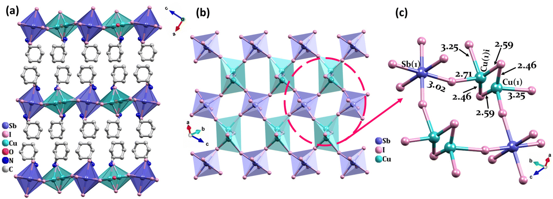 | ||
| Fig. 1 (a) The crystal structure of the 2D layered double perovskite CuSbI-1 (hydrogen atoms are omitted for clarity). (b) The platform of 2D inorganic layers consisting of alternating Cu–I6 octahedrons and Sb–I6 octahedrons. (c) The framework of the Cu–I–Sb octahedrons with different Cu–I and Sb–I bond lengths. (i): x, y − 1, z. | ||
The amino group of cyclohexylamine in the organic part is protonated, so each cyclohexylammonium ion has one positive charge. Due to the electrostatic interaction between the inorganic layer and the organic layer, the positively charged portion of the organic amine is toward the inorganic layer. As a consequence, CuSbI-1 exhibits many intermolecular hydrogen bonding interactions with the cations and water molecules of the type N–H⋯O listed in Table S4 in the ESI.†
Using a similar process, but replacing the cyclohexylamine group with cyclohexane-1,4-diamine, we obtained orange-red crystals of CuSbI-2 that crystallized in the monoclinic space group P21/n (Table S1, ESI†). The relevant crystallographic data are listed in Tables S5 and S6 in the ESI.† As shown in Fig. 2(a–c), CuSbI-2 also exhibits a 2D double perovskite structure. Obviously, the structure of CuSbI-2 is slightly different from that of CuSbI-1, with each inorganic layer being alternated with an organic layer of (NH3C6H10NH3)2+ cations. The inorganic part of CuSbI-2, is assembled to form a face by the vertex-sharing of [SbI6] and [CuI6] octahedra. Indeed, Sb–I bond lengths ranged from 2.827 (12) to 3.286 (12) Å, while, Cu–I bond lengths ranged from 2.542 (2) to 4.482 (2) Å. We noted that Cu–I bond lengths in CuSbI-2 are also quite different; the lengths of two Cu–I bonds which were vertical to the layer, were shorter. While, within the layer, the four equatorial Cu–I distances were much longer. The amino group of cyclohexane-1,4-diamine in the organic part is protonated, so each cyclohexane-1,4-diammonium ion has two positive charges. Due to the electrostatic interaction between the inorganic and organic layers, the amino groups with a positive charge at both ends of the cyclohexane-1,4-diammonium ion are close to the two inorganic counterparts (Table S7, ESI†). Thus, the cyclohexane-1,4-diammonium molecule is in a quasi-upright state.
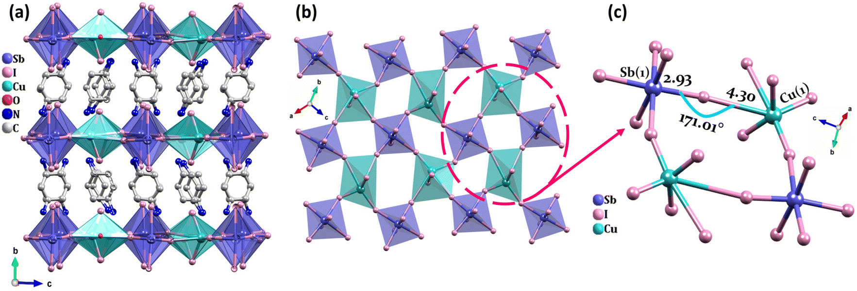 | ||
| Fig. 2 (a) The crystal structure of the 2D layered double perovskite CuSbI-2 (hydrogen atoms are omitted for clarity). (b) The platform of 2D inorganic layers consisting of alternating Cu–I6 octahedrons and Sb–I6 octahedra. (c) The framework of Cu–I–Sb octahedra with different Cu–I and Sb–I bond lengths. | ||
The bond length of Cu1–I9 (3.763 Å), Cu1–I11 (4.304 Å), Cu2–I2 (4.071 Å) and Cu2–I16 (4.482 Å) in CuSbI-2 are much longer than several reported complexes containing Cu–I bonds, such as 2.61–2.72 Å in (R/S-PCA)CuI2.46 Therefore, bonding characteristics of complexes CuSbI-1 and CuSbI-2 were investigated through the interaction region indicator (IRI) analysis47via Multiwfn program,48 which can distinguish the strengths and features of intra- or inter-molecular interactions in different regions. Reasonable fragments of both molecules were considered and their atomic coordinates were directly extracted from single crystal structures without geometry optimization (Fig. S1†). Before IRI analysis, density functional theory (DFT) calculations were performed by Gaussian 09![[thin space (1/6-em)]](https://www.rsc.org/images/entities/char_2009.gif) 49 in order to generate the stable wave functions of both fragments. Fig. 3 is the isosurface map of IRI = 0.9 for CuSbI-1 and CuSbI-2, and the function of sign(λ2)ρ is mapped on the isosurface, where ρ represents the electron density and λ2 is the second largest eigenvalue of the Hessian of ρ. The color bar ranging from blue to red corresponds to attractive and repulsive interactions with the increase of the sign(λ2)ρ value. Evidently, all C–C, C–H and Sb–I interactions belong to typical covalent and coordination bonds respectively, while for Cu(I) centers, two kinds of coordination bonds with different strengths can be observed, and the attractions between Cu(I) and I− ions correspond to their bond lengths.50,51 The much longer Cu–I bonds are so weak that they are comparable with vdW interactions, and such results demonstrate the formation of quasi-tetrahedral Cu(I) sites and two-dimensional structures for the whole system.
49 in order to generate the stable wave functions of both fragments. Fig. 3 is the isosurface map of IRI = 0.9 for CuSbI-1 and CuSbI-2, and the function of sign(λ2)ρ is mapped on the isosurface, where ρ represents the electron density and λ2 is the second largest eigenvalue of the Hessian of ρ. The color bar ranging from blue to red corresponds to attractive and repulsive interactions with the increase of the sign(λ2)ρ value. Evidently, all C–C, C–H and Sb–I interactions belong to typical covalent and coordination bonds respectively, while for Cu(I) centers, two kinds of coordination bonds with different strengths can be observed, and the attractions between Cu(I) and I− ions correspond to their bond lengths.50,51 The much longer Cu–I bonds are so weak that they are comparable with vdW interactions, and such results demonstrate the formation of quasi-tetrahedral Cu(I) sites and two-dimensional structures for the whole system.
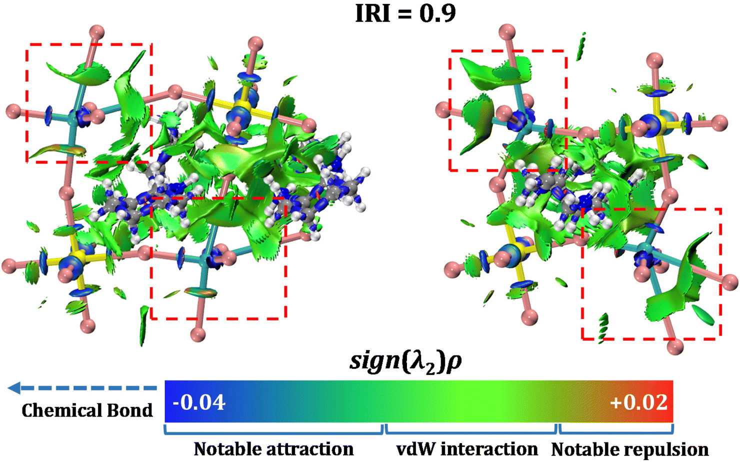 | ||
| Fig. 3 The isosurface map of the interaction region indicator (IRI) for CuSbI-1 (left) and CuSbI-2 (right). Colour codes: Cu, bluish-green; Sb, yellow; C, gray; I, pink; N, blue and H, white. | ||
To explore the composition of CuSbI-1 and CuSbI-2 along with the valence of copper, X-ray photoelectron spectroscopy (XPS) was performed. As shown in Fig. S2 in the ESI,† the XPS survey scan reveals principal peaks attributed to C 1s, N 1s, Sb 3d, I 3d, and Cu 2p for both compounds. Detailed high-resolution XPS spectra for CuSbI-1 and CuSbI-2 depicted the existence of two peaks of Cu 2p, each located near 952.0 eV and 931.5 eV, which are unique to the CuI ion and correspond to 2p1/2 and 2p3/2, respectively. Interestingly, XPS results are in well accordance with single crystal X-ray diffraction (SXRD) and prove the existence of CuI ions. Herein, it is worth noting here that CuI ions are not oxidized to CuII ions during the reaction, indicating the high stability of CuSbI-1 and CuSbI-2.
2.2 Optical properties
In order to estimate whether the compounds are suitable for optoelectronic applications, UV-vis diffuse reflectance spectra were recorded for CuSbI-1 and CuSbI-2, so that their optical band gaps could be determined. The results are displayed in Fig. 4(a and b). All the samples show typical band gap absorptions of semiconductors, which are around 500 nm for CuSbI-1 and CuSbI-2. The band gap energy (Eg) was estimated using the the Kubelka–Munk function:| F(R) = α/S = (1 − R)2/2R |
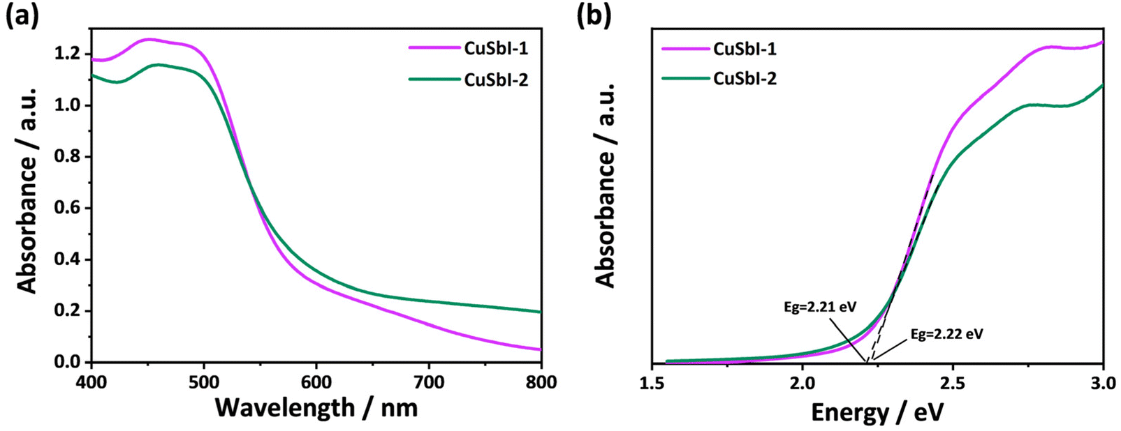 | ||
| Fig. 4 (a) UV-vis diffuse reflectance spectra of powdered CuSbI-1 and CuSbI-2. (b) Band gaps of powdered CuSbI-1 and CuSbI-2. | ||
2.3 Photo response properties
To further explore the application potential of the compounds in the field of optoelectronics, the photoconductivities of CuSbI-1 and CuSbI-2 were measured using pressed pellet samples with 10 V bias-voltages under 350 W solar-simulating xenon lamp irradiation. It can be clearly seen from Fig. 5a–d that the photo-generated currents of the two compounds are significantly higher than the current without an excitation light. Indeed, the ratio of the photocurrent to the dark current (Ilight/Idark) of CuSbI-1 and CuSbI-2 are about 23 and 10, respectively (Table S8, ESI†). Obviously, the two compounds have considerable photo responses under light illumination. Although their electrical conductivity is lower, their photo-response performance is much better, and the electric charge has a greater potential to be excited by light. In addition, the photocurrent presented a reproducible response, which could be observed for various consecutive on–off cycles under the same ambient conditions, suggesting that these materials have the potential for light detection.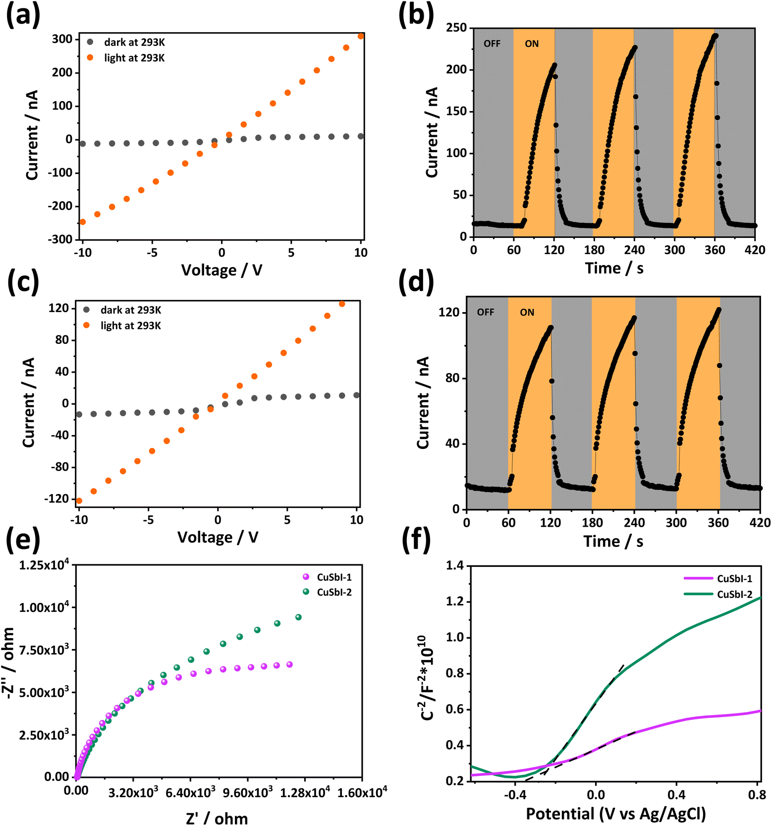 | ||
| Fig. 5 I–V plots for the dark and light current of CuSbI-1 (a) and CuSbI-2 (c) measured at 293 K under a 350 W xenon lamp. I–t plots of several irradiation cycles for CuSbI-1 (b) and CuSbI-2 (d). (e) EIS Nyquist plots of CuSbI-1 and CuSbI-2. (f) Mott–Schottky plots of CuSbI-1 and CuSbI-2. | ||
To gain an in-depth understanding of the separation efficiency of photogenerated electron–hole pairs in the materials, electrochemical impedance spectroscopy (EIS) tests were performed (Fig. 5e) and Nyquist plots were obtained. Obviously, the diameter of the plot of CuSbI-1 was significantly smaller than that of CuSbI-2, indicating that CuSbI-1 has a more efficient carrier separation ability. In addition, Mott–Schottky plots (Fig. 5f) of the compounds were also plotted, and the positive slopes confirmed the n-type semiconducting properties of CuSbI-1 and CuSbI-2. At the same time, it can be observed that the slope of CuSbI-1 in the Mott–Schottky plot is smaller than that of CuSbI-2, implying the higher carrier density of CuSbI-1.52–54
To further demonstrate the semiconducting nature of these materials, we plotted a series of I–V curves of the compounds by varying temperature from 30 °C to 80 °C (Fig. S4, ESI†). It can be seen that as the temperature increases from 30 °C to 80 °C, the electrical conductivity of CuSbI-1 and CuSbI-2 increases from 6.10 × 10⁻¹⁰ S cm−1 to 1.68 × 10⁻⁷ S cm−1 and 1.54 × 10⁻¹⁰ S cm−1 to 6.77 × 10⁻⁹ S cm−1, respectively (Table S9, ESI†). The analysis shows that the conductivity of CuSbI-1 and CuSbI-2 are temperature-dependent, indicating a typical semiconductor behavior. Using this feature, these two compounds can be used in temperature-dependent detectors or electrical devices operating at high-temperature environments.
2.4 Preparation and characterization of thin films
In order to further apply these two compounds as practical optoelectronic devices, thin films were obtained by spin coating 1 g mL−1 DMF solution of CuSbI-1 or CuSbI-2 on the ITO glass and annealing on a hot plate at 80 °C for 10 minutes and cooling to room temperature. Remarkably, both CuSbI-1 and CuSbI-2 are highly soluble in DMF as 1 ml DMF can dissolve more than 1 g crystals. Scanning electron microscopy (SEM) images shown in Fig. 6a–f demonstrated that the smooth, pinhole free, uniform CuSbI-1 and CuSbI-2 thin films covering the entire substrate are obtained. It also indicates that the two compounds can be easily made into thin films, which make it possible for them to be fabricated into thin-film devices. Moreover, as shown in Fig. S5(a–g) and S6(a–g) in the ESI,† the elemental mapping of CuSbI-1 and CuSbI-2 films shows that Cu, Sb, I, C, N, and O are uniformly and homogeneously distributed.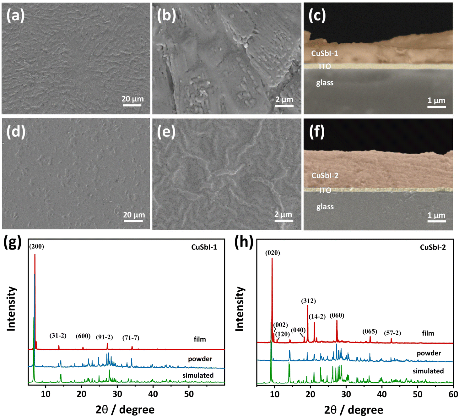 | ||
| Fig. 6 (a)–(c) SEM images of thin films formed by CuSbI-1 on ITO glass. (d)–(f) SEM images of thin films formed by CuSbI-2 on ITO glass. (g) and (h) XRD patterns of theoretical calculations of the compounds, powder diffraction, and thin films. | ||
In addition, to determine whether the prepared single crystal samples are pure and homogeneous with the phase of the corresponding single crystal compound. XRD measurements of single crystal powder samples and thin film samples were conducted, and then the results were compared with the simulated patterns (Fig. 6g and h). The results showed that there are no impurities in the prepared samples, and the diffraction peaks of the films coincide very well with powder counterparts, indicating that those compounds can be recrystallized back to original crystals after being spin-coated and annealed in the solvent.
Furthermore, in the most reported single-layer halide perovskites, inorganic layers grow parallel to the substrate surface.29 However, in this study, the XRD spectrum of the film of CuSbI-1 shows a strong (200) reflection, and that for CuSbI-2 shows a principal reflection of (020), which reveals the vertical growth of the compounds on the substrate.
Optical band gaps of the two films were obtained by UV-Vis DRS spectroscopy (Fig. S7(a and b), ESI†). The thin film band gaps of CuSbI-1 and CuSbI-2 are 2.38(3) eV and 2.33 (3) eV, respectively, which are slightly higher than the value of the corresponding powder samples (Fig. 4). This phenomenon, consistent with the works reported on (BA)4AgBiBr8, (BA)2CsAgBiBr8, Cs2AgBiBr6, (C6H16N2)2AgBiI8·H2O and (C6H16N2)2CuBiI8·0.5H2O, can be inferred to be caused by scattering according to the Mie theory.29,55
2.5 Stability characterization of materials
Improving the stability of perovskites used in devices has always been a scientific issue of concern because stability is a very important index in practical applications. In order to investigate the stability of both the synthesized perovskite compounds and the thin films, crystal powder samples were characterized by thermogravimetric analysis (TGA) as shown in Fig. S8.† Results indicated CuSbI-1 and CuSbI-2 do not show obvious mass loss until the temperature reached 260 °C and 320 °C respectively. They exhibit relatively better thermal stability than other Sb-based perovskites (Table S10, ESI†). Moreover, freshly prepared powders and thin films of CuSbI-1 and CuSbI-2 were stored at 55% relative humidity for 30 days. PXRD patterns of the powdered and thin film samples of CuSbI-1 and CuSbI-2 after the treatment showed no evidence of material decomposition (Fig. 7). The PXRD patterns of the samples after heating them at 100 °C in air for 72 h are also recorded, which confirmed their structural integrity. In other words, the two as-prepared perovskite materials are stable under high-temperature and humid environments.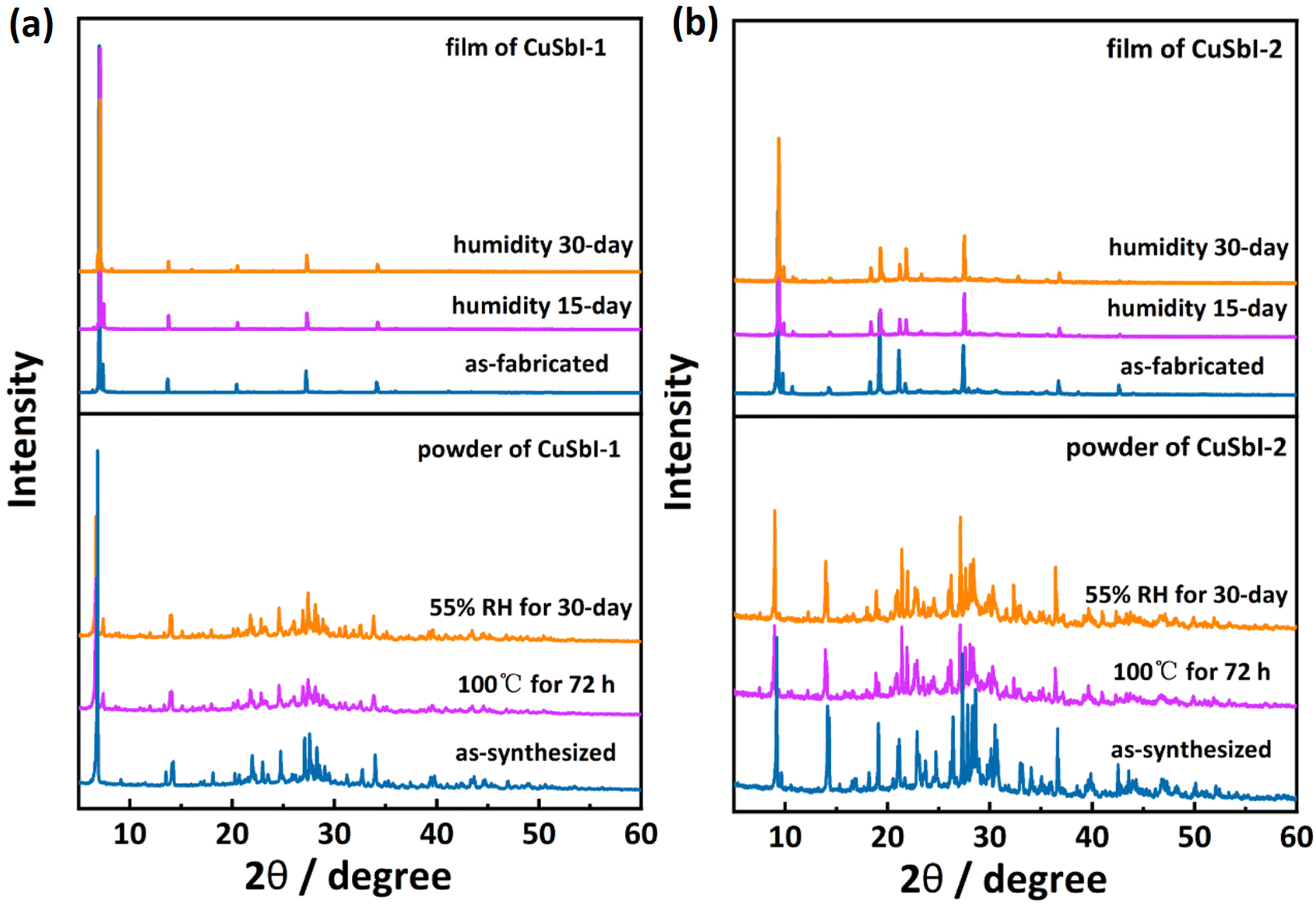 | ||
| Fig. 7 (a) PXRD patterns of the freshly prepared powdered sample of CuSbI-1, exposed to humidity (55% RH) for a month or heated at 100 °C for 72 hours; and PXRD patterns of the CuSbI-1 film before and after exposure to humidity (55% RH) for a month. (b) PXRD patterns of the freshly prepared powdered sample of CuSbI-2, exposed to humidity (55% RH) for a month or heated at 100 °C for 72 hours; and PXRD patterns of the CuSbI-2 film before and after exposure to humidity (55% RH) for a month. | ||
3. Conclusions
In summary, we have demonstrated that 2D Sb/Cu-based organic–inorganic hybrid bimetallic perovskite iodides can be obtained through the judicious selection of organic cations. Using cyclohexylamine and 1,4-cyclohexanediamine as the organic part, two 2D hybrid bimetallic perovskites CuSbI-1 and CuSbI-2, with a bandgap of 2.22(2) eV and 2.21(2) eV, respectively, have been successfully synthesized using the hydrothermal method. The temperature-dependent conductivity also reveals their semiconducting nature. Interestingly, the results of photoresponse characterization show that the photocurrent exhibited a stable and reproducible response. Pinhole-free and uniform thin films of the crystal samples can be fabricated by one-step spin coating, and the inorganic layers in the films were vertical to the substrates. Furthermore, both crystals and thin films present quite good stability and can be stable in hot and humid environments without decomposition. CuSbI-1 and CuSbI-2 with high moisture/thermal stability exhibit the potential for application in light detection and other optoelectronic fields.Conflicts of interest
There are no conflicts to declare.Acknowledgements
This work was supported by the NSFC (No. 21971203 and 11574244), the Key Scientific and Technological Innovation Team of Shaanxi Province (2020TD-001), the Xi'an Municipal Bureau of Science and Technology (201805056ZD7CG40), the State Key Laboratory for Mechanical Behavior of Materials (20212302), the Fundamental Research Funds for the Central Universities (xzy012020004) and the National Foreign Expert Program (QN2021170001L). We thank the Hefei Advanced Computing Center for computational support. We also thank the Instrument Analysis Center of Xi'an Jiaotong University.References
- K. T. A. Kojima, Y. Shirai and T. Miyasaka, J. Am. Chem. Soc., 2009, 131, 6050–6051 CrossRef PubMed.
- W. S. Yang, B. W. Park, E. H. Jung, N. J. Jeon, Y. C. Kim, D. U. Lee, S. S. Shin, J. Seo, E. K. Kim, J. H. Noh and S. I. Seok, Science, 2017, 356, 1376–1379 CrossRef CAS PubMed.
- F. Jiang, D. Yang, Y. Jiang, T. Liu, X. Zhao, Y. Ming, B. Luo, F. Qin, J. Fan, H. Han, L. Zhang and Y. Zhou, J. Am. Chem. Soc., 2018, 140, 1019–1027 CrossRef CAS PubMed.
- N. M. G. Xing, S. Sun, S. S. Lim, Y. M. Lam, M. Gratzel, S. Mhaisalkar and T. C. Sum, Science, 2013, 342, 344–347 CrossRef PubMed.
- C. S. Ponseca Jr., T. J. Savenije, M. Abdellah, K. Zheng, A. Yartsev, T. Pascher, T. Harlang, P. Chabera, T. Pullerits, A. Stepanov, J. P. Wolf and V. Sundstrom, J. Am. Chem. Soc., 2014, 136, 5189–5192 CrossRef PubMed.
- J. Cao, Y. M. Liu, X. Jing, J. Yin, J. Li, B. Xu, Y. Z. Tan and N. Zheng, J. Am. Chem. Soc., 2015, 137, 10914–10917 CrossRef CAS PubMed.
- S. De Wolf, J. Holovsky, S. J. Moon, P. Loper, B. Niesen, M. Ledinsky, F. J. Haug, J. H. Yum and C. Ballif, J. Phys. Chem. Lett., 2014, 5, 1035–1039 CrossRef CAS PubMed.
- W. J. Yin, T. Shi and Y. Yan, Adv. Mater., 2014, 26, 4653–4658 CrossRef CAS PubMed.
- M. Gratzel, Nat. Mater., 2014, 13, 838–942 CrossRef CAS PubMed.
- N. J. Jeon, J. H. Noh, Y. C. Kim, W. S. Yang, S. Ryu and S. I. Seok, Nat. Mater., 2014, 13, 897–903 CrossRef CAS PubMed.
- M. Yuan, L. N. Quan, R. Comin, G. Walters, R. Sabatini, O. Voznyy, S. Hoogland, Y. Zhao, E. M. Beauregard, P. Kanjanaboos, Z. Lu, D. H. Kim and E. H. Sargent, Nat. Nanotechnol., 2016, 11, 872–877 CrossRef CAS PubMed.
- X. Yang, X. Zhang, J. Deng, Z. Chu, Q. Jiang, J. Meng, P. Wang, L. Zhang, Z. Yin and J. You, Nat. Commun., 2018, 9, 570 CrossRef PubMed.
- Z. Liu, W. Qiu, X. Peng, G. Sun, X. Liu, D. Liu, Z. Li, F. He, C. Shen, Q. Gu, F. Ma, H. L. Yip, L. Hou, Z. Qi and S. J. Su, Adv. Mater., 2021, 33, e2103268 CrossRef PubMed.
- Y. Jia, R. A. Kerner, A. J. Grede, B. P. Rand and N. C. Giebink, Nat. Photonics, 2017, 11, 784–788 CrossRef CAS.
- S. A. Veldhuis, P. P. Boix, N. Yantara, M. Li, T. C. Sum, N. Mathews and S. G. Mhaisalkar, Adv. Mater., 2016, 28, 6804–6834 CrossRef CAS PubMed.
- B. S. Y. Kim, Y. Hikita, T. Yajima and H. Y. Hwang, Nat. Commun., 2019, 10, 5312 CrossRef PubMed.
- B. Jeong, L. Veith, T. Smolders, M. J. Wolf and K. Asadi, Adv. Mater., 2021, 33, e2100486 CrossRef PubMed.
- M. Ahmadi, T. Wu and B. Hu, Adv. Mater., 2017, 29, 1605242 CrossRef PubMed.
- R. Lyu, C. E. Moore, T. Liu, Y. Yu and Y. Wu, J. Am. Chem. Soc., 2021, 143, 12766–12776 CrossRef CAS PubMed.
- J. Zhou, J. Luo, X. Rong, P. Wei, M. S. Molokeev, Y. Huang, J. Zhao, Q. Liu, X. Zhang, J. Tang and Z. Xia, Adv. Opt. Mater., 2019, 7, 1900139 CrossRef.
- B. Su, J. Jin, Y. Peng, M. S. Molokeev, X. Yang and Z. Xia, Adv. Opt. Mater., 2022, 10, 2102619 CrossRef CAS.
- F. Igbari, Z. K. Wang and L. S. Liao, Adv. Energy Mater., 2019, 9, 1803150 CrossRef.
- P. P. Sun, Q. S. Li, L. N. Yang and Z. S. Li, Nanoscale, 2016, 8, 1503–1512 RSC.
- C. Zuo and L. Ding, Angew. Chem., Int. Ed., 2017, 56, 6528–6532 CrossRef CAS PubMed.
- Z. Deng, F. Wei, S. Sun, G. Kieslich, A. K. Cheetham and P. D. Bristowe, J. Mater. Chem. A, 2016, 4, 12025–12029 RSC.
- F. Wei, Z. Deng, S. Sun, F. Xie, G. Kieslich, D. M. Evans, M. A. Carpenter, P. D. Bristowe and A. K. Cheetham, Mater. Horiz., 2016, 3, 328–332 RSC.
- F. Wei, Z. Deng, S. Sun, F. Zhang, D. M. Evans, G. Kieslich, S. Tominaka, M. A. Carpenter, J. Zhang, P. D. Bristowe and A. K. Cheetham, Chem. Mater., 2017, 29, 1089–1094 CrossRef CAS.
- P. Li, W. Gao, C. Ran, H. Dong, X. Hou and Z. Wu, Phys. Status Solidi A, 2019, 216, 1900567 CrossRef CAS.
- L.-Y. Bi, Y.-Q. Hu, M.-Q. Li, T.-L. Hu, H.-L. Zhang, X.-T. Yin, W.-X. Que, M. S. Lassoued and Y.-Z. Zheng, J. Mater. Chem. A, 2019, 7, 19662–19667 RSC.
- T. T. Tran, J. R. Panella, J. R. Chamorro, J. R. Morey and T. M. McQueen, Mater. Horiz., 2017, 4, 688–693 RSC.
- T. Cai, W. Shi, S. Hwang, K. Kobbekaduwa, Y. Nagaoka, H. Yang, K. Hills-Kimball, H. Zhu, J. Wang, Z. Wang, Y. Liu, D. Su, J. Gao and O. Chen, J. Am. Chem. Soc., 2020, 142, 11927–11936 CrossRef CAS PubMed.
- L.-Y. Bi, T.-L. Hu, M.-Q. Li, B.-K. Ling, M. S. Lassoued, Y.-Q. Hu, Z. Wu, G. Zhou and Y.-Z. Zheng, J. Mater. Chem. A, 2020, 8, 7288–7296 RSC.
- M. S. Lassoued, L.-Y. Bi, Z. Wu, G. Zhou and Y.-Z. Zheng, J. Mater. Chem. C, 2020, 8, 5349–5354 RSC.
- M. S. Lassoued, L.-Y. Bi, Z. Wu, G. Zhou and Y.-Z. Zheng, Mater. Chem. Front., 2021, 5, 973–978 RSC.
- P. Vishnoi, R. Seshadri and A. K. Cheetham, J. Phys. Chem. C, 2021, 125, 11756–11764 CrossRef CAS.
- M. S. Lassoued, T. Wang, A. Faizan, Q.-W. Li, W.-P. Chen and Y.-Z. Zheng, J. Mater. Chem. C, 2022, 10, 12574–12581 RSC.
- M. Morana and L. Malavasi, Sol. RRL, 2021, 5, 2100550 CrossRef CAS.
- M. S. Lassoued, T. Wang, Q.-W. Li, X. Liu, W.-P. Chen, B. Jiaocd, Q.-Y. Yang, Z. Wu, G. Zhou, S. Ding, Z. Zhang and Y.-Z. Zheng, Mater. Chem. Front., 2022, 6, 2135–2142 RSC.
- J. Zhou, X. Rong, M. S. Molokeev, X. Zhang and Z. Xia, J. Mater. Chem. A, 2018, 6, 2346–2352 RSC.
- B. Vargas, E. Ramos, E. Perez-Gutierrez, J. C. Alonso and D. Solis-Ibarra, J. Am. Chem. Soc., 2017, 139, 9116–9119 CrossRef CAS PubMed.
- F. Wei, Z. Deng, S. Sun, N. T. P. Hartono, H. L. Seng, T. Buonassisi, P. D. Bristowe and A. K. Cheetham, Chem. Commun., 2019, 55, 3721–3724 RSC.
- J.-H. Wei, J.-F. Liao, L. Zhou, J.-B. Luo, X.-D. Wang and D.-B. Kuang, Sci. Adv., 2021, 7, eabg3989 CrossRef CAS PubMed.
- Y.-J. Li, T. Wu, L. Sun, R.-X. Yang, L. Jiang, P.-F. Cheng, Q.-Q. Hao, T.-J. Wang, R.-F. Lu and W.-Q. Deng, RSC Adv., 2017, 7, 35175–35180 RSC.
- K. Z. Du, W. Meng, X. Wang, Y. Yan and D. B. Mitzi, Angew. Chem., Int. Ed., 2017, 56, 8158–8162 CrossRef CAS PubMed.
- G. Volonakis, M. R. Filip, A. A. Haghighirad, N. Sakai, B. Wenger, H. J. Snaith and F. Giustino, J. Phys. Chem. Lett., 2016, 7, 1254–1259 CrossRef CAS PubMed.
- X. Ji, S. Geng, S. Zhang, Y. Gong, X. Zhang, R. Li, Y. Liu, J. Chen, R. Chen, Z. Xiao and L. Mao, Chem. Mater., 2022, 34, 8262–8270 CrossRef CAS.
- T. Lu and Q. Chen, Chem.: Methods, 2021, 1, 231–239 CAS.
- T. Lu and F. Chen, J. Comput. Chem., 2012, 33, 580–592 CrossRef CAS PubMed.
- M. J. Frisch, G. W. Trucks, H. B. Schlegel, G. E. Scuseria, M. A. Robb, J. R. Cheeseman, G. Scalmani, V. Barone, B. Mennucci, G. A. Petersson, H. Nakatsuji, M. Caricato, X. Li, H. P. Hratchian, A. F. Izmaylov, J. Bloino, G. Zheng, J. L. Sonnenberg, M. Hada, M. Ehara, K. Toyota, R. Fukuda, J. Hasegawa, M. Ishida, T. Nakajima, Y. Honda, O. Kitao, H. Nakai, T. Vreven, J. A. Montgomery Jr., J. E. Peralta, F. Ogliaro, M. Bearpark, J. J. Heyd, E. Brothers, K. N. Kudin, V. N. Staroverov, R. Kobayashi, J. Normand, K. Raghavachari, A. Rendell, J. C. Burant, S. S. Iyengar, J. Tomasi, M. Cossi, N. Rega, N. J. Millam, M. Klene, J. E. Knox, J. B. Cross, V. Bakken, C. Adamo, J. Jaramillo, R. Gomperts, R. E. Stratmann, O. Yazyev, A. J. Austin, R. Cammi, C. Pomelli, J. W. Ochterski, R. L. Martin, K. Morokuma, V. G. Zakrzewski, G. A. Voth, P. Salvador, J. J. Dannenberg, S. Dapprich, A. D. Daniels, ö. Farkas, J. B. Foresman, J. V. Ortiz, J. Cioslowski and D. J. Fox, Gaussian 09, Gaussian, Inc., Wallingford, CT, 2009 Search PubMed.
- Y. Yuan, J. Yang, Z. Liu, R. Tan, M. Chuai, J. Sun, Y. Xu, X. Zheng, M. Wang, T. Ahmad, N. Chen, Z. Zhu, K. Li and W. Chen, Adv. Energy Mater., 2022, 12, 2103705 CrossRef CAS.
- B. S. Aweke, C. H. Yu, M. Zhi, W. C. Chen, G. P. A. Yap, L. Zhao and T. G. Ong, Angew. Chem., Int. Ed., 2022, 61, e202201884 CAS.
- S. Yang, C. Liu, H. Li, S. Wang, J. Choi and L. Li, Energy Storage Mater., 2021, 39, 278–286 CrossRef.
- X. Zheng, L. Feng, Y. Dou, H. Guo, Y. Liang, G. Li, J. He, P. Liu and J. He, ACS Nano, 2021, 15, 13209–13219 CrossRef CAS.
- L. Xia, W. Zhou, Y. Xu, Z. Xia, X. Wang, Q. Yang, G. Xie, S. Chen and S. Gao, Chem. Eng. J., 2023, 451, 138747 CrossRef CAS.
- B. A. Connor, L. Leppert, M. D. Smith, J. B. Neaton and H. I. Karunadasa, J. Am. Chem. Soc., 2018, 140, 5235–5240 CrossRef CAS PubMed.
Footnote |
| † Electronic supplementary information (ESI) available. CCDC 2143410 and 2143411. For ESI and crystallographic data in CIF or other electronic format see DOI: https://doi.org/10.1039/d2nr06996b |
| This journal is © The Royal Society of Chemistry 2023 |