
 Open Access Article
 This Open Access Article is licensed under a Creative Commons Attribution-Non Commercial 3.0 Unported Licence
Plasma-jet printing of colloidal thermoelectric Bi2Te3 nanoflakes for flexible energy harvesting†
Jacob
Manzi‡
 af,
Ariel E.
Weltner‡
bc,
Tony
Varghese‡
ab,
Nicholas
McKibben
b,
Mia
Busuladzic-Begic
b,
David
Estrada
bcde and
Harish
Subbaraman
*acdf
af,
Ariel E.
Weltner‡
bc,
Tony
Varghese‡
ab,
Nicholas
McKibben
b,
Mia
Busuladzic-Begic
b,
David
Estrada
bcde and
Harish
Subbaraman
*acdf
aDepartment of Electrical and Computer Engineering, Boise State University, Boise, ID 83725, USA
bMicron School of Materials Science and Engineering, Boise State University, Boise, ID 83725, USA
cCenter for Atomically Thin Multifunctional Coatings, Boise State University, Boise, ID 83725, USA
dCenter for Advanced Energy Studies, Boise State University, Boise, ID 83725, USA
eIdaho National Laboratory, Idaho Falls, ID 83416, USA
fSchool of Electrical Engineering and Computer Science, Oregon State University, Corvallis, OR 97333, USA. E-mail: harish.subbaraman@oregonstate.edu
First published on 21st February 2023
Abstract
Thermoelectric generators (TEGs) convert temperature differences into electrical power and are attractive among energy harvesting devices due to their autonomous and silent operation. While thermoelectric materials have undergone substantial improvements in material properties, a reliable and cost-effective fabrication method suitable for microgravity and space applications remains a challenge, particularly as commercial space flight and extended crewed space missions increase in frequency. This paper demonstrates the use of plasma-jet printing (PJP), a gravity-independent, electromagnetic field-assisted printing technology, to deposit colloidal thermoelectric nanoflakes with engineered nanopores onto flexible substrates at room temperature. We observe substantial improvements in material adhesion and flexibility with less than 2% and 11% variation in performance after 10![[thin space (1/6-em)]](https://www.rsc.org/images/entities/char_2009.gif) 000 bending cycles over 25 mm and 8 mm radii of curvature, respectively, as compared to previously reported TE films. Our printed films demonstrate electrical conductivity of 2.5 × 10³ S m−1 and a power factor of 70 μW m−1 K−2 at room temperature. To our knowledge, these are the first reported values of plasma-jet printed thermoelectric nanomaterial films. This advancement in plasma jet printing significantly promotes the development of nanoengineered 2D and layered materials not only for energy harvesting but also for the development of large-scale flexible electronics and sensors for both space and commercial applications.
000 bending cycles over 25 mm and 8 mm radii of curvature, respectively, as compared to previously reported TE films. Our printed films demonstrate electrical conductivity of 2.5 × 10³ S m−1 and a power factor of 70 μW m−1 K−2 at room temperature. To our knowledge, these are the first reported values of plasma-jet printed thermoelectric nanomaterial films. This advancement in plasma jet printing significantly promotes the development of nanoengineered 2D and layered materials not only for energy harvesting but also for the development of large-scale flexible electronics and sensors for both space and commercial applications.
 Jacob Manzi | Jacob Manzi is a Ph.D. student in the School of Electrical Engineering and Computer Science at Oregon State University. He received his B.S. in Physics at Northwest Nazarene University. His research interests include additive manufacturing for flexible hybrid electronic applications, 2D materials, and printed device characterization. More specifically, his research focuses on plasma-jet printing of electronic materials for in-space manufacturing. |
 Ariel E. Weltner | Ariel Weltner received her B.S. and M.S. in Materials Science and Engineering from Boise State University. During her M.S. her research focused on solution synthesis and additive manufacturing of bismuth telluride nanoflakes. Currently, she is a product manager at Micron Technology, Inc. |
 Tony Varghese | Dr Tony Valayil Varghese is a Research Scientist in Electrical and Computer Engineering at Boise State University. He received his Ph.D. degree in Material Science and Engineering from Boise State University in 2019. His research focuses on additive manufacturing of nanomaterials for flexible energy harvesting and wearable and flexible hybrid electronics. |
 Nicholas McKibben | Nicholas McKibben is a 5th year Ph.D. student in materials science and engineering at Boise State University. He is a classically trained chemist who received his B.S. in Chemistry from Northwest Nazarene University and began his graduate studies in inorganic chemistry at Texas Tech University. Nick is currently working in the Advanced Nanomaterials and Manufacturing Laboratory under the tutelage of Dr David Estrada. His primary area of research is additive manufacturing, with specific interest in nanoparticle ink development and sensor fabrication. |
 Mia Busuladzic-Begic | Mia Busuladzic-Begic is an undergraduate student at Brown University. While at Boise High School, she worked at the Advanced Nanomaterial and Manufacturing Laboratory as a research assistant in Dr David Estrada's and Dr Harish Subbaraman's research group. During her time at Boise State University, she worked in synthesizing materials and conducting experiments, gathering stability and rheology data on several co-solvent systems to improve the morphology of printed black phosphorus thin films. Additionally, she analyzed additively manufactured thermoelectric films and participated in nanomaterial synthesis and characterization. |
 David Estrada | Dr David Estrada is an associate professor of Materials Science and Engineering at Boise State University. He is the Associate Director for the Center of Advanced Energy Studies, Deputy Director of Academic Research at Idaho National Laboratory, and the Site Director of the NSF IUCRC Center for Atomically Thin Multifunctional Coatings. He received his M.S. in Electrical Engineering 2009 and his Ph.D. in Electrical Engineering in 2013 from the University of Illinois at Urbana-Champaign, under the direction of Professor Eric Pop. His research interests are in the areas of emergent additive manufacturing, semiconductor nanomaterials, and bionanotechnology. |
 Harish Subbaraman | Harish Subbaraman earned the M.S. and Ph.D. degrees in electrical engineering from The University of Texas at Austin in 2006 and 2009, respectively. Until 2016, he worked as a Senior Research Scientist at Omega Optics, Inc (Austin, TX), where he led and managed several SBIR/STTR projects in the areas of printed and flexible hybrid electronics and silicon/polymer photonics. In 2016, he joined The Department of Electrical and Computer Engineering at Boise State University (Boise, ID). At Boise State, he served as the Associate Site Director for NSF I/UCRC (ATOMIC) and the Advanced Manufacturing BSU lead for the Center for Advanced Energy Studies. He joined The School of Electrical Engineering and Computer Science at Oregon State University in Fall 2022, where he is currently an Associate Professor. He has published in over 200 refereed journals and conferences. He is a senior member of IEEE. |
Introduction
Integrated energy harvesters for flexible hybrid electronics are in high demand following advancements in lower power consumption electronic devices for Internet of Things (IoT) and wearable electronics.1–3 Flexible thermoelectric generators (TEGs) integrated into heat sources such as radioisotope thermoelectric generators (RTG) are ideal candidates as energy sources in space industries and microgravity environments. Flexible TEGs offer many advantages over various energy harvesting methods, including long-term reliability, lightweight and not requiring sunlight to operate, offering a longer mission lifetime. They are insensitive to the extreme cold and high radiation fields in space and have no moving parts involved in producing uninterrupted power using available temperature differences.4,5 The ability of thermoelectric materials to convert heat energy into electrical energy can be described by a dimensionless figure of merit,| ZT = S2σT/κ | (1) |
Metal chalcogenides, such as bismuth telluride (Bi2Te3), are commonly used materials for low-temperature TEGs due to their superior ZT at room temperature.6,7 There have been many attempts to develop Bi2Te3 nanoparticle-based flexible TEGs using nanostructuring to improve the Seebeck coefficient and reduce thermal conductivity.8–10 The topological behavior of these materials offers high surface mobility of charge carriers in the nanocrystal due to the non-parabolic band structure, demanding precise control of nanomaterial morphology and thickness to improve thermoelectric performance.11 Phonons typically have a longer mean free path compared to electrons, allowing particle and grain size engineering to be used as a mechanism for enhancing ZT by optimizing the σ/κ ratio.12,13 It has been shown that solvothermal synthesis temperature can be used to introduce a single nanopore in the center of Bi2Te3 nanoflakes.14,15 It is possible that these nanopores will improve thermoelectric properties by acting as an additional scattering site for phonons.
While precise control of nanostructure and morphology of metal chalcogenide materials has been studied extensively to improve ZT values, a scalable and reliable manufacturing method for flexible TEGs with good mechanical and thermoelectric properties remains a challenge. Namely, improved adhesion between the thermoelectric material and substrate is required to improve device performance. A common approach is to apply chemical or plasma treatment to the substrate surface, however, this introduces limitations when integrating the substrate with flexible hybrid electronic (FHE) devices. Additionally, it adds an undesirable step in the fabrication process of flexible TEGs.
Additive manufacturing (AM) offers many advantages for the fabrication of TEG and FHE devices, including rapid processing speeds, design flexibility, and the ability to convert colloidal suspensions into functional devices.16,17 Recently, many AM modalities have been developed for the fabrication of thermoelectric films by direct deposition of colloidal inks. Direct writing18,19 screen printing6,20 inkjet printing21 and aerosol jet printing22,23 have shown promise as scalable and cost-effective methods for fabricating flexible TEGs compared to other processes, such as thermal evaporation, vacuum filtration, and spray coating. Despite these advances, current AM methods are inadequate for meeting the needs of device manufacturing in microgravity environments and/or in situ plasma-assisted chemical modification of surfaces or inks.
Here we report the use of a novel plasma-assisted and gravity-independent printing technique for developing TEGs with direct conversion of nanomaterials into flexible devices with improved adhesion and high resolution. Plasma-jet printing is a new AM technology that has been shown to sinter metal nanoparticles in situ, reduce material oxidation states, promote substrate adhesion, and increase packing density.24–26 The use of a dielectric barrier discharge (DBD) plasma in the plasma-jet printer enables atmospheric printing of nanomaterial films without the need for expensive vacuum equipment. DBD plasmas have been shown to assist in etching and deposition of materials, modification of surface energy, and oxidizing, reducing, and removing organic films.27,28 Atmospheric plasma jets have been shown to operate both by electrical phenomenon and plasma flow, enabling high flow directionality independent of gravity.28,29
Recently, plasma-jet printing of nanomaterial inks onto flexible substrates has been demonstrated with carbon nanotubes,25 silver nanowires,26 metal oxide nanoparticles,24,30 and graphene oxide.31,32 In this work, we present the first reporting to our knowledge of plasma-jet printed thermoelectric nanoparticles. The development of this new printing technology opens up novel opportunities for integrating flexible energy harvesters in self-powered electronic devices and marks significant progress in developing AM technologies for microgravity and space environments.
Thermoelectric ink synthesis
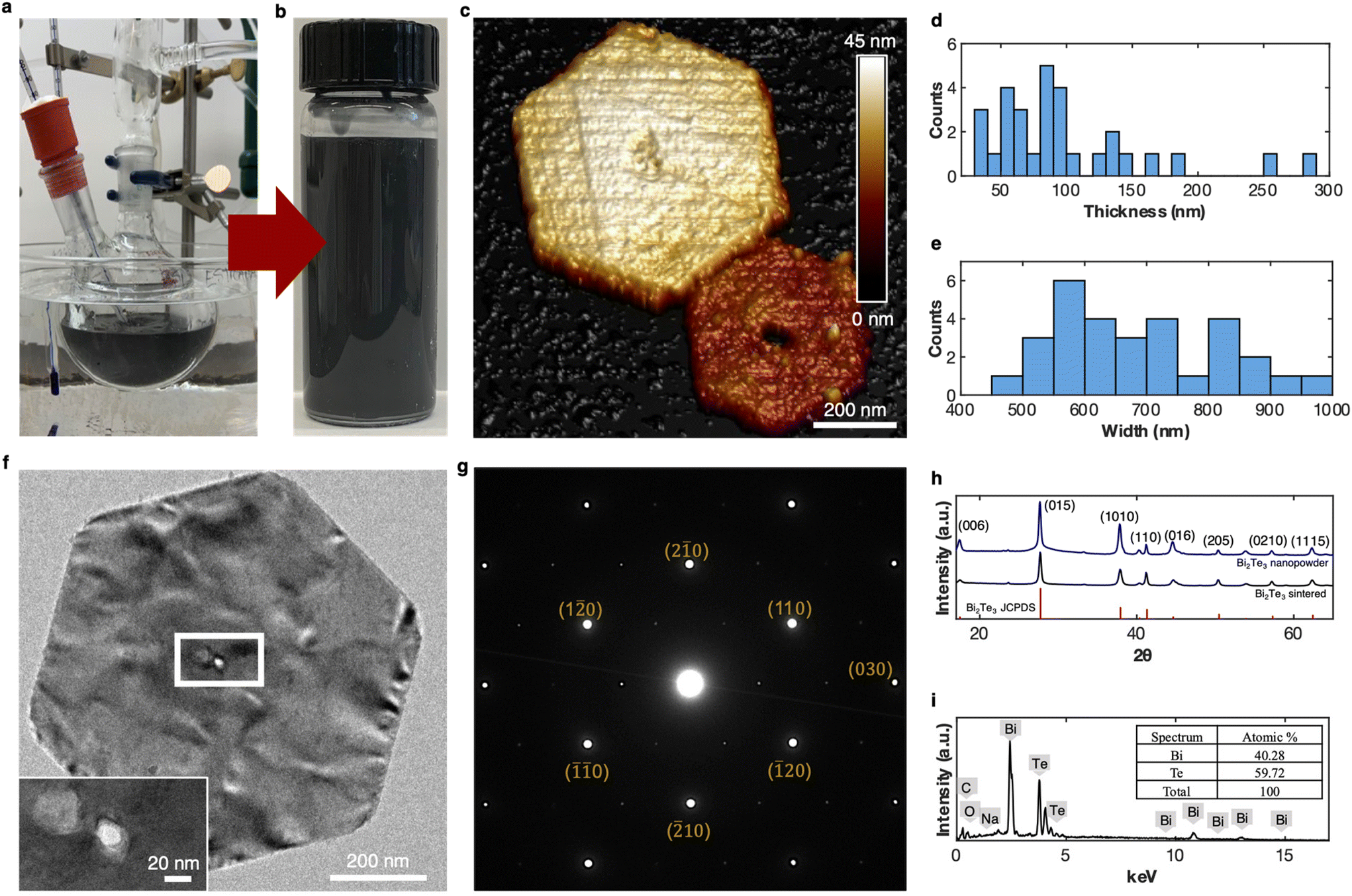 | ||
| Fig. 1 Synthesis and characterization of Bi2Te3 nanoflakes. Optical images of (a) solvothermal synthesis process and (b) as-synthesized thermoelectric ink dispersed in a cosolvent system. (c) Atomic force microscopy rendering of representative nanoflakes. (d and e) Histograms of lateral width and thickness of flakes from AFM. (f) Transmission electron microscopy image with inset showing the nanopore in the center of the nanoflake. (g) SAED pattern of the imaged rhombohedral Bi2Te3 nanoflake indexed in yellow to the [00l] zone-axis. (h) X-ray diffraction of Bi2Te3 powder and sintered film. (i) Energy dispersive spectroscopy scan of as-printed Bi2Te3 films. | ||
![[3 with combining macron]](https://www.rsc.org/images/entities/char_0033_0304.gif) m, no. 166. The crystal structure is comprised of five alternating layers of covalently bonded tellurium and bismuth atoms, forming a quintuple layer Te(1)–Bi–Te–Bi–Te(1). These quintuple layers stack due to weak electrostatic interactions, and a van der Waals bond forms between the Te(1)–Te(1) atoms of adjacent quintuple layers. These unique crystallographic features result in lattice parameters with a higher than usual c/a ratio. The unit cell, or one monolayer, consists of three stacked quintuple layers, with reported lattice parameters of c = 3.045 and a,b = 0.438 nm.34 The anisotropy of the unit cell and nanometer dimensionality of the particles are largely credited for the excellent thermoelectric properties exhibited by this material.15 TEM imaging of a well-defined hexagonal particle shows an edge length of 420 nm and a particle width of 840 nm (Fig. 1f).
m, no. 166. The crystal structure is comprised of five alternating layers of covalently bonded tellurium and bismuth atoms, forming a quintuple layer Te(1)–Bi–Te–Bi–Te(1). These quintuple layers stack due to weak electrostatic interactions, and a van der Waals bond forms between the Te(1)–Te(1) atoms of adjacent quintuple layers. These unique crystallographic features result in lattice parameters with a higher than usual c/a ratio. The unit cell, or one monolayer, consists of three stacked quintuple layers, with reported lattice parameters of c = 3.045 and a,b = 0.438 nm.34 The anisotropy of the unit cell and nanometer dimensionality of the particles are largely credited for the excellent thermoelectric properties exhibited by this material.15 TEM imaging of a well-defined hexagonal particle shows an edge length of 420 nm and a particle width of 840 nm (Fig. 1f).
A magnified image of the two nanopores intrinsic to this Bi2Te3 nanoflake is shown as the inset, with measured pore sizes of 20 and 35 nm. Dimensions of the nanoflakes measured by TEM were in good agreement with the statistical data acquired from AFM for particle and pore size. A selected area electron diffraction pattern was generated for the imaged hexagonal nanoflake, zone-axis [000l] (Fig. 1g). The material was phase pure and single crystalline in nature with a hexagonal symmetry pattern. Powder X-Ray diffraction was also performed to confirm bulk purity (Fig. 1h), and the d-spacing of the 110 peak was calculated to be 0.219 nm, which is confirmed by SAED and supported by existing literature.34
The rheological properties of Bi2Te3 dispersed in the cosolvent inks were extensively studied (Table 1). The alcohol component of the cosolvent system was varied to determine the optimal cosolvent composition. The alcohols are present in the exact same ratio compared to the other co-solvent chemicals. The cosolvent system containing ethanol demonstrated superior stability compared to the other ink composition, as indicated by the nanoparticles staying dispersed in solution even after one week while the other cosolvent inks had sedimented completely (Fig. S2†). The viscosity and surface tension of the various inks in Table 1 are similar and within the plasma-jet printer's allowed parameters. In comparison, the mean contact angle varies significantly with alcohol type. Due to the method of printing, the high contact angle of the ink is not a barrier; however, further tuning of the ink composition would be necessary to make the cosolvent system compatible with drop-on-demand printing modalities, such as inkjet printing offering multi-printer compatible inks.
:ethylene glycol:alcohol is the same for each composition
| Water:ethylene glycol:ethanol |
Water:ethylene glycol:isopropanol |
Water:ethylene glycol:2-butanol |
|
|---|---|---|---|
| Mean contact angle (°) | 48.49 | 41.31 | 19.14 |
| Mean viscosity (cP) | 2.648 | 2.912 | 2.985 |
| Surface tension (mN m−1) | 37.05 | 33.52 | 27.18 |
Printer optimization and film fabrication
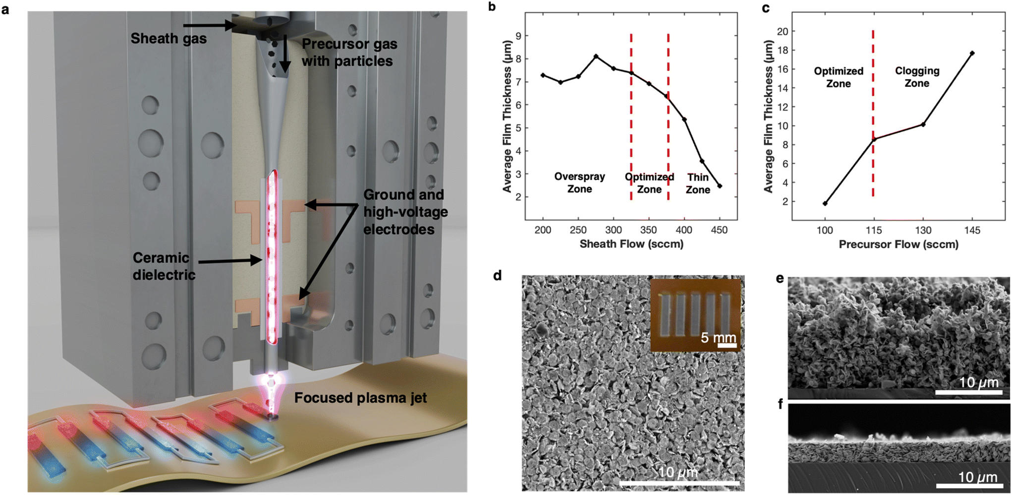 | ||
| Fig. 2 Print and film optimization. (a) Schematic diagram of the PJP printhead. Average thickness by (b) sheath flow and (c) precursor flow showing optimized conditions. (d) Top-down scanning electron microscopy image of the printed film (inset) after mechanical pressing. Cross sectional SEM of the printed film (e) as printed and (f) after pressing and sintering. | ||
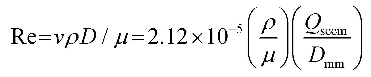
In the plasma-jet system during operation, the atomized particles are carried by the precursor flow through the helium plasma and then through a 0.5 mm nozzle. The helium sheath gas surrounds the particles in the nozzle and is used to generate the plasma. The optimal precursor-to-sheath gas ratio is ∼1:3.5. To optimize the printer for the thermoelectric colloidal ink for plasma jet printing, a series of 0.2 × 10 mm long lines were printed with sheath flow ranging from 200 to 450 sccm at a constant precursor gas flow of 100 sccm (Fig. 2b and c). These lines were evaluated using a Nikon optical microscope and Bruker DektakXT stylus profilometer to determine flow that optimizes the film thickness while minimizing overspray. With increasing sheath gas flow, the average thickness of the printed line decreases (Fig. 2b). When the flow is above the optimal zone, the film thickness decreases. The width of the line also decreases as more of the material does not adhere to the substrate because of the higher pressure from the increased gas flow. Below the optimal zone, the printed line becomes quite wide with overspray and has a non-ideal and non-uniform pointed cross-section. The optimal zone for the sheath flow was chosen to achieve an optimal film thickness with minimal overspray.
Additionally, the precursor gas was varied from 100 to 145 sccm, and a series of 10 mm lines were printed holding the sheath gas at 300 sccm. With increasing precursor flow, the average film thickness increases (Fig. 2c). This is expected since more atomized particles will be directed to the printhead and deposited with higher precursor flow. While printing, it was noted that after about 120 sccm, the nozzle would clog in about 20 minutes, which is not ideal for long print times or printing multiple TE legs on the same substrate. The optimal zone was chosen from 100–120 sccm precursor flow where a sufficient amount of material is deposited while mitigating the printhead clog. After printing, the films were mechanically pressed to densify the films and improve contact between nanoflakes for better electrical conductivity.6,20 A top-down SEM image of a printed film after pressing and sintering highlights the hexagonal structures packed on the substrate (Fig. 2d). Cross-sectional SEMs of the films before (Fig. 2e) and after pressing and sintering (Fig. 2f) show the thickness is reduced from about 14 μm to 4 μm.
 | (2) |
 | (3) |
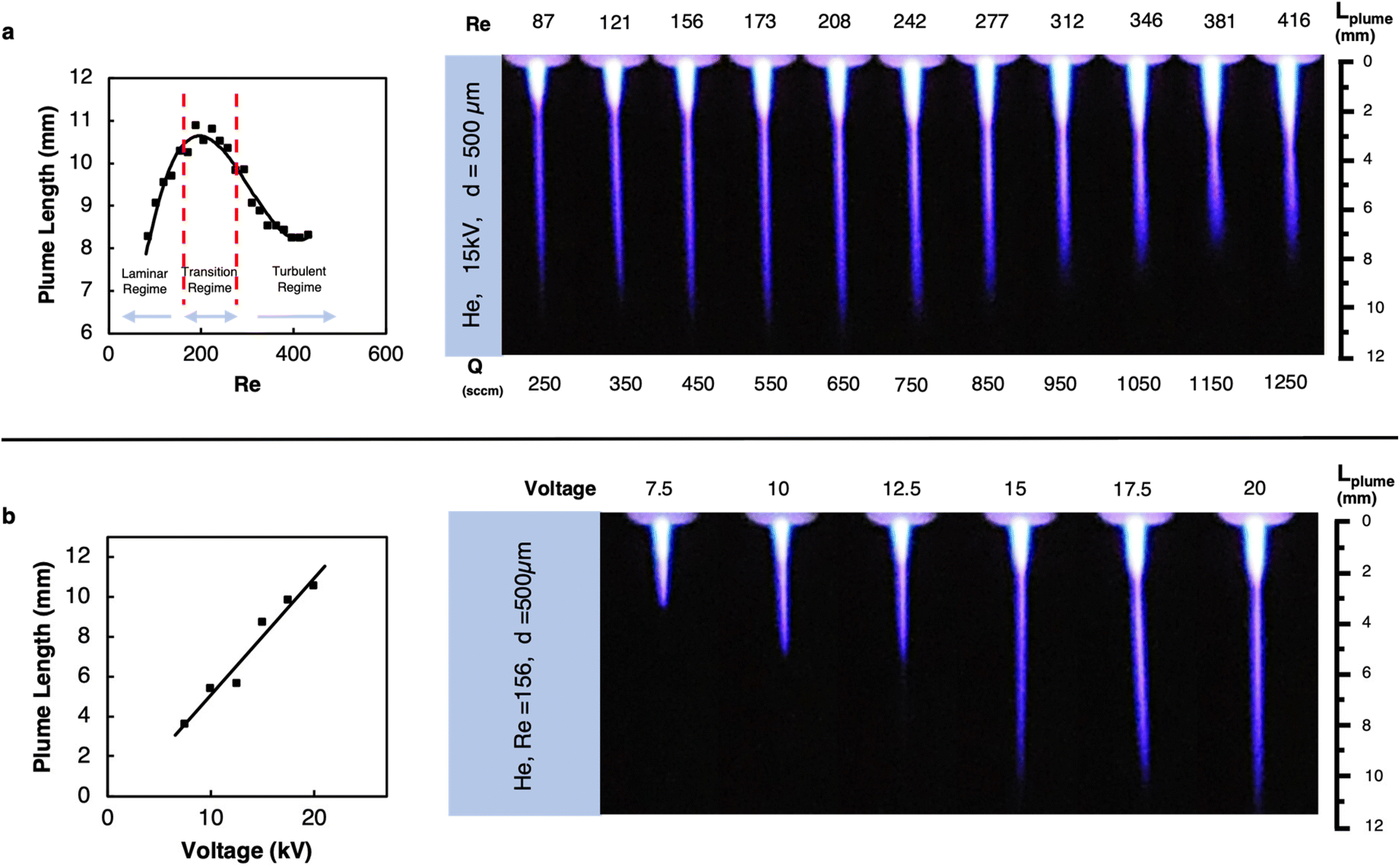 | ||
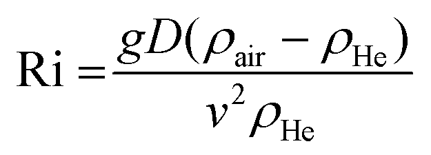
| Fig. 3 Fluid dynamics of the plasma plume. (a) Plasma plume length vs. Reynolds number showing the laminar, transition, and turbulent regimes. Corresponding optical images of plume length with Reynold's number above and total helium flow below each plume. (b) Plasma plume length vs. plasma voltage. Corresponding optical images of plume length vs. power supply voltage for Re = 156. | ||
Thermoelectric film analysis
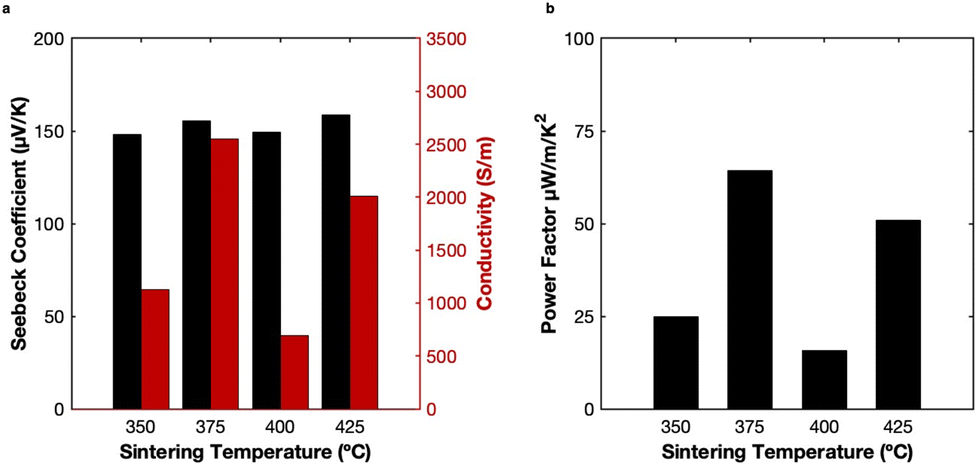 | ||
| Fig. 4 Electrical and thermoelectric properties. (a) Seebeck coefficient and electrical conductivity and (b) power factor (S2σ) after thermal sintering. | ||
| Material | Deposition method | S (μV K−1) | σ (S m−1) | PF (μW m−1 K−2) | Ref. |
|---|---|---|---|---|---|
| Bi2Te3 | PJP | −155 | 2500 | 70 | This Work |
| PEDOT:PSS + 50 wt% Bi2Te3 | AJP | 17 | 350 | 15 | 45 |
| Bi2Te2.7Se0.3 | AJP | −78 | 44500 |
270 | 46 |
| Bi2Te2.7Se0.3 | AJP | −163 | 27000 |
730 | 23 |
| Bi2Te3 | AJP | −64 | 940 | 3.85 | 22 |
| Bi2Te1.7Se0.3 | IJP | ∼−161 | ∼6200 | ∼160 | 47 |
| Bi0.5Sb1.5Te3 | IJP | ∼207 | ∼1400 | ∼60 | 47 |
| Bi2Te3 | IJP | ∼119 | ∼5600 | ∼78 | 21 |
| Bi0.5Sb1.5Te3 | IJP | ∼72 | ∼34000 |
∼154 | 21 |
The electrical conductivity is an order of magnitude lower than the conventional bulk Bi2Te3 thermoelectric material at room temperature. The cross-sectional SEM images (Fig. 2e and f) show a highly porous network of nanocrystals resulting in high interface resistance, hence lower electrical conductivity. The large porosity formation in the printed films is due to random stacking of nanoplates as they adhere to the polyimide substrate22 as well as potentially trapping the burn-off residues from the interaction of plasma with the surface capping agents on the nanocrystals. The interaction of plasma ions with the nanomaterial capping agents causes the burning of the polymer capping, resulting in a highly porous stacking of nanocrystals. Optimization of the plasma energies is also essential in improving the density and uniformity of the thin films. With no plasma on, few nanoflakes are deposited, and the glass slide is visible through the material (Fig. S5†). When the plasma is turned on and maintained at 15 kV, a thick layer of nanoflakes is deposited, and the packing density is high. Interestingly, when the plasma voltage is increased to 20 kV, the thickness increases, but the packing density decreases as many voids are formed throughout the material (Fig. S5†). Lower electrical conductivities are also due to the lower sintering conditions of the printed films, limited by the melting point of polymer substrates.
To quantify the as-printed porosity and sintering densification of the films, Gwyddion was used to threshold map the SEM images of the film cross-sections (Fig. 2e and f). The threshold mask was set to 20%, and the relative area function was used to find percentage porosity. Blue masks are displayed over the pores in the film before and after pressing and sintering (Fig. S6a and b†). Before pressing and sintering, the relative area porosity of the film was 38%, and the film was not conductive. After pressing and sintering, the porosity of the film was reduced to 7%.
000 bending cycles to understand the material property changes. The formation of cracks and delamination of the printed films can be easily detected with a rapid increase in resistance with respect to bending, and hence, electrical resistance was chosen to understand the flexibility of the printed films. As the bending radius changes, the resistance of the printed films increases (Fig. 5a), with a maximum of 11% increase in resistance after 10000 bending for 8 mm ROC, demonstrating excellent flexibility of the films. In the case of 25 mm ROC, only a 2% change in resistance was observed after 10000 bends, indicating the superior adhesion and flexibility of plasma-assisted printed 2D thin films on flexible substrates.
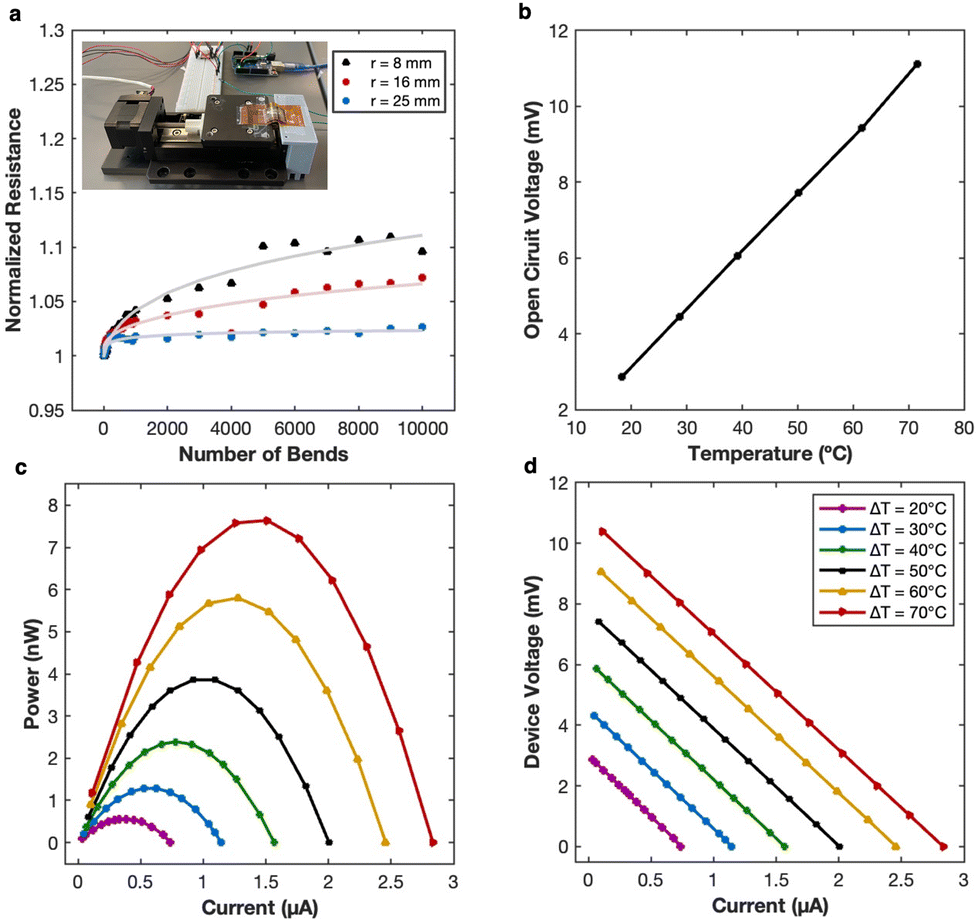 | ||
| Fig. 5 Electrical characterization of single leg TE film sintered at 425 °C. (a) Resistance as a function of bending cycles for various radii of curvature. Inset shows bending test apparatus. (b) Open circuit voltage as a function of temperature difference, (c) device voltage as a function of current and (d) power curves for several temperature differentials. | ||
The output voltage and power of a single PJP-printed thermoelectric leg was measured (Fig. 5b–d). The output power and device voltage show promise for the development of small-scale flexible thermoelectric generators with superior flexibility for powering low-power electronic devices. When open-circuit voltage (VOC) is measured as a function of temperature difference (ΔT) (Fig. 5b), the device VOC increases linearly with ΔT by virtue of the Seebeck effect, achieving a maximum output voltage of 11 mV at a 70 °C temperature difference. This high VOC and Seebeck coefficient for a single leg is due to the defect-induced nanostructuring of the Bi2Te3 crystals. The device operating voltage and power output as a function of electrical current were tested at different temperature differences, respectively (Fig. 5c and d). A single leg thermoelectric device with a maximum power of over 7 nW was obtained with a ΔT of 70 °C when an external load is resistance matched with the internal resistance of the leg. The performance of a single leg thermoelectric device (Fig. 5d) shows promising opportunities for large-scale, highly flexible devices for low-power applications.
Conclusions
We report the first demonstration of scalable, plasma-jet printed, 2D colloidal nanomaterial inks for flexible and low-cost thermoelectric device fabrication for microgravity and zero-gravity environments. Defect-engineered nanoflakes with adjustable pore size at the center were developed using a scalable solvothermal synthesis process. Detailed ink characterization was performed to optimize ink stability and ink-substrate interactions developing a general ink formulation for novel plasma-jet printing opportunities. An exploration into the fluid dynamics of the commercial plasma-jet printer was performed, and printing parameters within the laminar region of plasma flow were determined. The samples sintered at 375 °C showed a power factor of 70 μW m−2 K−1 and a change in resistance of 2% after 10000 cycles of bending with a 25 mm ROC. A single-leg thermoelectric device developed using PJP on a flexible, polyimide substrate produced 7 nW of power with a temperature gradient of 70 °C. These results mark significant advancement in developing plasma-jet printing of nanomaterial-based devices with superior flexibility and adhesion for microgravity and zero gravity applications.
Materials and methods
Chemicals
Bismuth nitrate pentahydrate (Bi(NO3)3H2O, >99.9%), sodium tellurite (Na2TeO3, >99.5%), sodium hydroxide (NaOH, >99%), poly(vinyl) pyrrolidone (PVP, MW 40000) and ethylene glycol were purchased from Fisher Scientific. All chemicals were used as received.
Solution synthesis of nanoparticles
In a standard reaction, 0.2 mmol Bi(NO3)3H2O (0.0970 g), 0.3 mmol Na2TeO3 (0.0665 g), 4 mmol NaOH (0.1600 g), and 2 mmol PVP (0.2223 g) was combined with 10 mL ethylene glycol in a 25 mL double-neck flask. The mixture was stirred for 15 minutes using a magnetic stir bar to fully dissolve all solids before equipping with a reflux condenser and heating in an oil bath to 190 °C (Fig. 1a). After three hours, the flask was removed from the oil bath and allowed to cool to room temperature naturally. 20 mL isopropanol (IPA) and 10 mL acetone were added to the mixture, followed by centrifugation at 20000 rpm (37560g) for 16 minutes at 20 °C. The supernatant was discarded, and the collected solids were redispersed in IPA by bath sonication. The washing steps were repeated two more times to remove excess ethylene glycol, PVP, and other impurities. The final product was dried over a hot plate and massed before dispersing in a water-based co-solvent system to form the colloidal ink.
Plasma-jet printing and thermal sintering
Thermoelectric ink was printed using a commercial helium PJP from Space Foundry (Model #sfas000000074 28) onto polyimide (Kapton®) substrates that had been wiped with IPA. The nozzle size was 0.5 mm in diameter, and the print head was set at a height of 2 mm from the substrate. The samples were printed in 2 × 12 mm rectangles filled with a serpentine pattern of 50 μm spacing. Printed layers varied from 1–3 at a speed of 0.5–1 mm s−1. The atomizer power was set to 40% and the sheath, and precursor gasses were varied from 325–375 sccm and 100–150 sccm between print sessions, respectively. The plasma voltage parameters were set to 12–15 kV and 27.6 kHz, the resonant frequency of the printhead used. These parameters were optimized during each session of printing for good adhesion, sufficient film thickness, uniform coverage, and minimal overspray. After printing, the films were dried on a hot plate in an ambient atmosphere at 150 °C for one hour to remove any remaining solvent. The dried samples were compacted using a cold hydraulic press using two thin layers of mica sheets as the cover plates with pressure up to 40 MPa. Thermal sintering was performed in a commercial tube furnace in an inert atmosphere. The peak temperature varied from 300 °C to 425 °C with a 60-minute sintering duration. The sintering temperature was limited because of the low degradation temperature of 50 μm Kapton substrates.Atomic force microscope characterization
Bi2Te3 nanoflakes were imaged using a Bruker Dimension Icon atomic force microscope (AFM) under atmospheric conditions. Imaging was performed using a ScanAsyst-Air probe (Bruker, 2 nm radius of curvature) operating in PeakForce Tapping mode. Thirty nanoflakes were imaged to derive statistics. The height of each nanoflake was recorded as the peak value from the substrate, excluding any particulates present. Width measurements were obtained for each of the three pairs of sides on the hexagonal nanoflake and averaged to report the lateral dimensions.Scanning electron microscope characterization
Scanning electron microscopy was used to image the topography of the plasma-deposited thermoelectric films. A Field Emission Scanning Electron Microscope (FEI Teneo) under high vacuum was used for imaging and EDS elemental analysis. The ETD and T1 detectors were used to obtain varying resolutions in imaging the deposited material.Transmission electron microscope characterization
Bi2Te3 nanoflake ink was diluted in isopropyl alcohol and mixed using ultrasonication. The dispersion was drop cast onto a 300-mesh carbon-coated copper TEM grid for characterization using a JEOL 2100 HR TEM operating at 200 kV. Brightfield and high-resolution imaging were performed on the sample, and a selected area diffraction pattern was generated from a fully formed Bi2Te3 nanoflake.Ink rheology measurements
Surface tension and contact angle were measured using a Biolin Scientific Attension optical tensiometer. Viscosity was measured using a Brookfield Ametek rheometer. Both measurements were performed for each cosolvent system with a particle concentration of 20 mg mL−1.Flexibility testing
The mechanical flexibility and durability of the films after bending were tested using an automated flexibility testing apparatus. The custom flexibility testing machine was constructed using a Micronix USA Translation Stage VT-50L controlled by an Arduino Uno. A base and stationary platform were 3D printed using a stereolithography (SLA) printer to match the height of the stage (Fig. 5a). The thermoelectric leg was placed on a supporting piece of polyimide and taped over the gap between the linear stage and the printed stationary platform. By controlling the number of steps and direction the stepper motor moves, the gap between the stage decreased and increased, causing the film to bend. The thermoelectric legs could be repeatedly bent to a precise radius using a set number of steps determined experimentally. Static bend tests were performed for three different ROC of 8, 16, and 25 mm. The resistance of the samples was measured after each bend test. The testing was performed at intervals of 10 bends until 100 total bends, then intervals of 100 bends until 1000 total bends, and then intervals of 1000 bends until 10000 total bends were achieved. This ensured that the change in resistance of the film from the initial bends was captured more finely than the change in resistance from the latter bends when damage was done, and resistance change was minimal. The normalized resistance was plotted against the number of bends for each radius of curvature, and the curves were fit with exponential trend lines.
Electrical characterization
Conductivity measurements were performed using a linear four-point probe method with an inner probe spacing of 6 mm. A 100 mA current was passed through the sample, and five measurements were taken of the voltage difference of the center probes. The resistance was calculated using Ohm's law, and the average resistance was determined for each sample. The conductivity was calculated using the average thickness and width from the stylus profilometry of the films to find the cross-sectional area. The conductivity for each leg and sintering temperature was calculated and recorded.Thermoelectric characterization
Seebeck coefficients and power measurements were performed on a custom testbed built using two commercial Peltier modules, one operating as a heater and the other as a cooler. The hot side and cold side of the TE leg were thermally grounded to the Peltier modules to create a temperature gradient. Two E-type thermocouples were mounted with voltage probes on the hot and cold sides with soft indium contacts to measure the temperature and voltage. For better contacts and measurements, an insulating layer was used to thermally insulate and apply pressure at the thermocouples. The device was connected electrically in series to the shunt resistor and a variable resistor for impedance matching at each measurement temperature. The device's open-circuit voltage, load voltage, current, and power output were measured at each temperature difference.Author contributions
J. M. optimized the printer, fabricated the flexible films descriptions and performed out SEM, flexibility and electrical characterization. A. W. and T. V. synthesized the thermoelectric material and ink. A. W. optimized and performed ink characterization, and performed AFM. N. M. performed the TEM, XRD, and crystallography analysis. M. B., T. V. A. W. carried out thermoelectric property characterization on the films. D. E., H. S., T. V. and J. M. contributed to the conceptualization of this work. D. E. and H. S. supervised the project and H. S. is the PI.Conflicts of interest
There is no conflicts to declare.Acknowledgements
The authors acknowledge funding support from the National Aeronautics and Space Administration EPSCoR (grant # 80NSSC19M0151), National Science Foundation IUCRC Phase II (award # 2113873), National Science Foundation (award # CMMI-1825502), and Idaho Commerce IGEM (award # 3732018). The authors would like to acknowledge staff and students of the Surface Science Lab at Boise State University for their advice and assistance. A. W. acknowledges support through the Department of Energy's University Nuclear Leadership Program Graduate Research Fellowship. The graphical abstract was partially created with BioRender.com.References
- S. Xu and W. Wu, Adv. Intell. Syst., 2020, 2, 2000117 CrossRef.
- A. Proto, J. Vondrak, M. Schmidt, J. Kubicek, O. M. Gorjani, J. Havlik and M. Penhaker, IEEE Access, 2021, 9, 20878–20892 Search PubMed.
- R. Wei, S. Yan, Z. Dongliang, A. Ablimit, Z. Shun, S. Chuanqian, Z. Jialun, G. Huiyuan, Z. Jie, Z. Lixia, X. Jianliang and Y. Ronggui, Sci. Adv., 2021, 7, eabe0586 CrossRef PubMed.
- H. Goldsmid, Thermoelectric Refrigeration, Springer, US, 1964 Search PubMed.
- D. M. Rowe, CRC Handbook of Thermoelectrics, CRC press, 1995 Search PubMed.
- T. Varghese, C. Dun, N. Kempf, M. Saeidi-Javash, C. Karthik, J. Richardson, C. Hollar, D. Estrada and Y. Zhang, Adv. Funct. Mater., 2020, 30, 1905796 CrossRef CAS.
- M. M. Mallick, A. G. Rösch, L. Franke, A. Gall, S. Ahmad, H. Geßwein, A. Mazilkin, C. Kübel and U. Lemmer, J. Mater. Chem. A, 2020, 8, 16366–16375 RSC.
- R. J. Mehta, Y. Zhang, C. Karthik, B. Singh, R. W. Siegel, T. Borca-Tasciuc and G. Ramanath, Nat. Mater., 2012, 11, 233–240 CrossRef CAS PubMed.
- K. Biswas, J. He, I. D. Blum, C.-I. Wu, T. P. Hogan, D. N. Seidman, V. P. Dravid and M. G. Kanatzidis, Nature, 2012, 489, 414–418 CrossRef CAS PubMed.
- M. S. Dresselhaus, G. Chen, M. Y. Tang, R. G. Yang, H. Lee, D. Z. Wang, Z. F. Ren, J.-P. Fleurial and P. Gogna, Adv. Mater., 2007, 19, 1043–1053 CrossRef CAS.
- C. Dun, W. Kuang, N. Kempf, M. Saeidi-Javash, D. J. Singh and Y. Zhang, Adv. Sci., 2019, 6, 1901788 CrossRef CAS PubMed.
- P. Bed, H. Qing, M. Yi, L. Yucheng, M. Austin, Y. Bo, Y. Xiao, W. Dezhi, M. Andrew, V. Daryoosh, C. Xiaoyuan, L. Junming, M. S. Dresselhaus, C. Gang and R. Zhifeng, Science, 2008, 320, 634–638 CrossRef PubMed.
- M. Scheele, N. Oeschler, K. Meier, A. Kornowski, C. Klinke and H. Weller, Adv. Funct. Mater., 2009, 19, 3476–3483 CrossRef CAS.
- C. Dun, C. A. Hewitt, Q. Jiang, Y. Guo, J. Xu, Y. Li, Q. Li, H. Wang and D. L. Carroll, Chem. Mater., 2018, 30, 1965–1970 CrossRef CAS.
- Y. Hosokawa, K. Tomita and M. Takashiri, Sci. Rep., 2019, 9, 10790 CrossRef PubMed.
- K. Fukuie, Y. Iwata and E. Iwase, Micromachines, 2018, 9 Search PubMed.
- M. M. Mallick, A. G. Rösch, L. Franke, S. Ahmed, A. Gall, H. Geßwein, J. Aghassi and U. Lemmer, ACS Appl. Mater. Interfaces, 2020, 12, 19655–19663 CrossRef CAS PubMed.
- A. Chen, D. Madan, M. Koplow, P. K. Wright and J. W. Evans, PowerMEMS, Washington DC, USA, 2009 Search PubMed.
- A. Chen, D. Madan, P. K. Wright and J. W. Evans, J. Micromech. Microeng., 2011, 21, 104006 CrossRef.
- T. Varghese, C. Hollar, J. Richardson, N. Kempf, C. Han, P. Gamarachchi, D. Estrada, R. J. Mehta and Y. Zhang, Sci. Rep., 2016, 6, 33135 CrossRef CAS PubMed.
- B. Chen, M. Kruse, B. Xu, R. Tutika, W. Zheng, M. D. Bartlett, Y. Wu and J. C. Claussen, Nanoscale, 2019, 11, 5222–5230 RSC.
- C. Hollar, Z. Lin, M. Kongara, T. Varghese, C. Karthik, J. Schimpf, J. Eixenberger, P. H. Davis, Y. Wu, X. Duan, Y. Zhang and D. Estrada, Adv. Mater. Technol., 2020, 5, 2000600 CrossRef CAS PubMed.
- M. Saeidi-Javash, W. Kuang, C. Dun and Y. Zhang, Adv. Funct. Mater., 2019, 29, 1901930 CrossRef.
- A. Dey, A. Lopez, G. Filipič, A. Jayan, D. Nordlund, J. Koehne, S. Krishnamurthy, R. P. Gandhiraman and M. Meyyappan, J. Vac. Sci. Technol., B: Nanotechnol. Microelectron.: Mater., Process., Meas., Phenom., 2019, 37, 31203 Search PubMed.
- R. P. Gandhiraman, E. Singh, D. C. Diaz-Cartagena, D. Nordlund, J. Koehne and M. Meyyappan, Appl. Phys. Lett., 2016, 108, 123103 CrossRef.
- R. P. Gandhiraman, V. Jayan, J.-W. Han, B. Chen, J. E. Koehne and M. Meyyappan, ACS Appl. Mater. Interfaces, 2014, 6, 20860–20867 CrossRef CAS PubMed.
- G. S. Selwyn, H. W. Herrmann, J. Park and I. Henins, Contrib. Plasma Phys., 2001, 41, 610–619 CrossRef CAS.
- M. Teschke, J. Kedzierski, E. G. Finantu-Dinu, D. Korzec and J. Engemann, IEEE Trans. Plasma Sci., 2005, 33, 310–311 Search PubMed.
- D. H. Gutierrez, P. Doshi, D. Nordlund and R. P. Gandhiraman, Flexible Printed Electron., 2022, 7, 25016 CrossRef.
- R. Ramamurti, R. P. Gandhiraman, A. Lopez, P. Doshi, D. Nordlund, B. Kim and M. Meyyappan, IEEE Open J. Nanotechnol., 2020, 1, 47–56 Search PubMed.
- Y. Wang, K. Zhang, R. Wang, C. Zhang, F. Kong and T. Shao, J. Mater. Sci.: Mater. Electron., 2019, 30, 8944–8954 CrossRef CAS.
- A. Dey, S. Krishnamurthy, J. Bowen, D. Nordlund, M. Meyyappan and R. P. Gandhiraman, ACS Nano, 2018, 12, 5473–5481 CrossRef CAS PubMed.
- A. Subrati, Y. Kim, Y. Al Wahedi, V. Tzitzios, S. Alhassan, H. J. Kim, S. Lee, E. Sakellis, N. Boukos, S. Stephen, S. M. Lee, J. B. Lee, M. Fardis and G. Papavassiliou, CrystEngComm, 2020, 22, 7918–7928 RSC.
- D. Kong, W. Dang, J. J. Cha, H. Li, S. Meister, H. Peng, Z. Liu and Y. Cui, Nano Lett., 2010, 10, 2245–2250 CrossRef CAS PubMed.
- M. Pinchuk, O. Stepanova, N. Kurakina and V. Spodobin, J. Phys.: Conf. Ser., 2017, 830, 12060 CrossRef.
- D. J. Jin, H. S. Uhm and G. Cho, Phys. Plasmas, 2013, 20, 83513 CrossRef.
- A. H. Basher and A.-A. H. Mohamed, J. Appl. Phys., 2018, 123, 193302 CrossRef.
- Q. Xiong, X. Lu, K. Ostrikov, Z. Xiong, Y. Xian, F. Zhou, C. Zou, J. Hu, W. Gong and Z. Jiang, Phys. Plasmas, 2009, 16, 43505 CrossRef.
- K. Yambe, S. Taka and K. Ogura, IEEJ Trans. Electr. Electron. Eng., 2014, 9, S13–S16 CAS.
- E. R. Subbarao and B. J. Cantwell, J. Fluid Mech., 1992, 245, 69–90 CrossRef CAS.
- R. P. Satti and A. K. Agrawal, Int. J. Heat Fluid Flow, 2006, 27, 336–347 CrossRef.
- E. Karakas, M. Koklu and M. Laroussi, J. Phys. D: Appl. Phys., 2010, 43, 155202 CrossRef.
- P. A. Leptuch and A. K. Agrawal, J. Visualization, 2006, 9, 101–109 CrossRef CAS.
- R. Xiong, Q. Xiong, A. Y. Nikiforov, P. Vanraes and C. Leys, J. Appl. Phys., 2012, 112, 33305 CrossRef.
- C. Ou, A. L. Sangle, A. Datta, Q. Jing, T. Busolo, T. Chalklen, V. Narayan and S. Kar-Narayan, ACS Appl. Mater. Interfaces, 2018, 10, 19580–19587 CrossRef CAS PubMed.
- T. V. Varghese, Ph.D.Thesis, Boise State University, 2019 Search PubMed.
- Z. Lu, M. Layani, X. Zhao, L. P. Tan, T. Sun, S. Fan, Q. Yan, S. Magdassi and H. H. Hng, Small, 2014, 10, 3551–3554 CrossRef CAS PubMed.
Footnotes |
| † Electronic supplementary information (ESI) available. See DOI: https://doi.org/10.1039/d2nr06454e |
| ‡ These authors contributed equally. |
| This journal is © The Royal Society of Chemistry 2023 |