
 Open Access Article
 This Open Access Article is licensed under a
 Creative Commons Attribution 3.0 Unported Licence
Uniaxial strain tuning of organic molecule single photon sources
Anastasios
Fasoulakis
ab,
Kyle D.
Major
a,
Rowan A.
Hoggarth
 a,
Paul
Burdekin
a,
Dominika P.
Bogusz
a,
Ross C.
Schofield
a and
Alex S.
Clark
*ac
a,
Paul
Burdekin
a,
Dominika P.
Bogusz
a,
Ross C.
Schofield
a and
Alex S.
Clark
*ac
aCentre for Cold Matter, Blackett Laboratory, Imperial College London, Prince Consort Road, SW7 2AZ, London, UK. E-mail: alex.clark@bristol.ac.uk
bQuantum Engineering Centre for Doctoral Training, University of Bristol, 5 Tyndall Avenue, BS8 1FD, Bristol, UK
cQuantum Engineering Technology Labs, H. H. Wills Physics Laboratory and Department of Electrical and Electronic Engineering, University of Bristol, BS8 1UB, Bristol, UK
First published on 15th November 2022
Abstract
Organic fluorophores are excellent single photon sources, combining high brightness, lifetime-limited linewidths and useful emission wavelengths. A key factor in their performance as photon emitters is their dynamic frequency tunability, which can be used to render the emission from multiple molecules indistinguishable. In this work we demonstrate dynamic tuning of dibenzoterrylene molecules embedded in anthracene crystals through the application of uniaxial strain fields. By bending a piezoelectric strip in two opposite directions in linear steps, we impose an escalating compressive or tensile strain on the molecular crystals, resulting in two opposite dynamic detunings of the dopant dibenzoterrylene emission wavelength. To validate that the tuning mechanism is strain, we performed a similar measurement using an identical strip that was depolarised by annealing in which the tuning was absent. Finally, we simulated the effect of strain on the dopant dibenzoterrylene emission wavelength by combining molecular dynamics and density functional theory techniques to determine the strain tuning rate which matched well with that found experimentally.
1 Introduction
Integrated photonics is a promising platform for exploiting the quantum behaviour of light on a chip for quantum technology applications.1 Most efforts in this area exploit the quantum nature of single photon states. Therefore, making quantum photonics useful for practical applications demands bright, stable single photon sources. The indistinguishability of the generated photons is essential in many quantum technology schemes, for example, in various quantum key distribution protocols2 and optical quantum computing schemes.3 Consequently, if photons from multiple sources need to interact, the ability to tune independent sources into resonance with each other becomes important.A promising approach for achieving single photon sources is fluorescent organic molecules that can absorb and emit photons. These fluorophores can be doped into organic crystals to form a host–guest ensemble, held together by intermolecular van der Waals forces. In these systems the coupling between the fluorescent molecules and vibronic modes is relatively suppressed and the main dephasing mechanism is caused by liberation of the molecules themselves.4,5 Consequently, spectral diffusion was decreased resulting in lifetime-limited emission at low temperatures. Dibenzoterrylene is a widely used fluorophore and can be embedded in para-dichlorobenzene,6para-terphenyl,7 or, as we use in this work, anthracene (Ac) crystals. DBT in Ac emits photons between 780 nm and 795 nm, which, when cooled down to a temperature below 3 K, have narrow linewidths of around 50 MHz.8,9 Furthermore, DBT-doped Ac crystals can be easily grown with a highly controlled level of the dopant concentration and the morphology of the generated crystals10 can be engineered to result in bright, stable single photon sources11 capable of emitting indistinguishable photons.12
A key factor in using indistinguishable photons for obtaining quantum information is the ability to dynamically tune the sources to resonate with each other, allowing for interference.13 In most types of quantum emitters this has been based on engineering the energy gap of the emission transition either through the use of the Stark effect or through the application of strain on the material containing them.14–18 The mechanism of strain tuning is based on the deformation of the molecule which changes the wave function and electronic potential. This does not affect the highest occupied molecular orbital (HOMO) and the lowest unoccupied molecule orbital (LUMO) identically, hence the energy gap between them changes. This is the energy gap of the emission transition. Previously, the effect of pressure induced strain has been studied in pentacene molecules embedded in p-terphenyl crystals.19,20 Also, acoustic strain has been applied to DBT-doped Ac crystals which resulted in a modulation of the fluorescence from molecules.21 In this paper, we show a reversible dynamical tuning of DBT single photon sources through the application of controlled uniaxial strain on the crystals’ geometry. We analysed the effect of this strain on the linewidth distribution of molecules and performed a similar experiment on a substrate that has been annealed to remove the piezoelectricity. To support our results theoretically, we also carried out simulations to estimate the tuning rate that emerges per unit of strain which is in good agreement with our observations.
2 Experimental methods
2.1 Crystal growth
DBT-doped Ac crystals were grown using a co-sublimation technique, detailed in ref. 10. An example crystal is shown in Fig. 1b. The growth took place inside a vapour deposition chamber with independent temperature control of the two crucibles containing DBT and Ac, respectively. Fine tuning of these temperatures allowed for a specific dense DBT-doping within the Ac crystal. After the growth process, a single crystal of several microns thick and a millimeter across was placed onto the strain setup.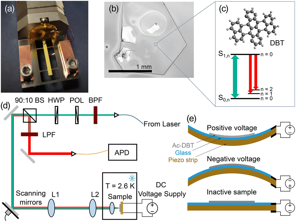 | ||
| Fig. 1 (a) Photograph of a piezoelectric strip containing a molecular crystal. As the strip bends, unidirectional strain is enforced on the crystal. The strain direction deviates from the crystal a axis by 10°. (b) White light microscope image of an anthracene crystal doped with dibenzoterrylene (DBT) molecules. (c) Molecular structure of DBT and a Jablonski diagram of the ground (S0) and the first excited (S1) states. Carbon atoms are shown in dark gray and hydrogen atoms in light gray. (d) Cryogenic confocal microscope setup. See the main text for details. (e) Depiction of the strain mechanism in our experiment. Positive voltage on the active piezoelectric strip compelled it to bend downwards, resulting in a compression of the molecular crystal. Negative voltage compelled it to bend upwards, leading to a decompression of the crystal. Finally, the positive voltage on the inactive sample did not enforce any strain on the emitters. | ||
2.2 Strain setup
We used a piezoelectric crystal to apply strain to the Ac crystals in a controlled and reproducible way. A photograph of this setup is shown in Fig. 1a, while it is presented schematically in Fig. 1e. A piezoelectric bending strip (RS PRO, EB-T-320), consisting of two piezo crystals sandwiched together, was fastened at both ends to a stainless steel mount. When a positive voltage was applied, the bending strip became concave (or convex for a negative voltage). An Ac crystal selected from the above growth process was placed on a 150 μm thick polished glass layer, attached to the bending piezo. The lateral dimensions of the glass layer were matched with those of the piezoelectric strip, which were ∼15 mm × 1.5 mm. The crystal was held in place using a poly-vinyl acetate (PVA) coating, which also protected the crystal from sublimation or oxygen intrusion. This setup transferred the movement of the bending piezo to either a contraction or stretching of the crystal, placing the molecules under compressive or tensile strain.To isolate the effects of strain on the DBT emission from possible Stark tuning14 (due to the application of an electric field) we used a second strip with no piezoelectric effect. This inactive sample was identical to the above strip; however, it was heated to 600 K for two hours before mounting to depolarise the material and effectively remove the bending motion when a voltage is applied.
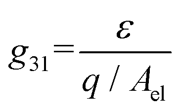
To calculate the amount of strain that we expected to apply per unit V, we used the piezoelectric voltage constant, defined as22
 | (1) |
 | (2) |
Using the values found on the piezoelectric strip technical specifications22 of C = 795 pf and g31 = 12.1 mV m N−1, we estimated a strain of 4.03 × 10⁻⁵% per V for a strip at room temperature without the layer of glass on top. Based on previous measurements conducted on similar piezoelectric elements, we estimated that at 2.6 K the generated strain should be 10 times lower than at room temperature. Also, after measuring the resonant frequency of its mechanical oscillations with and without the glass, we found that the glass increased the equivalent force constant k by 30%, which should impose a similar reduction in strain. These factors reduce the expected strain to 2.81 × 10⁻⁶% per V.
2.3 Optical setup
All optical measurements were conducted in the confocal microscope setup shown in Fig. 1d. A continuous-wave (cw) Ti:sapphire laser (MSquared, SolsTiS) was used for the excitation of DBT. The laser was coupled onto the table using a polarisation maintaining fibre and collimated using an aspheric lens. The beam passed through a polariser and a 785(5) nm band pass filter (BPF) to clean up the polarisation and remove any unwanted background light from the fibre, before passing through a half-wave plate (HWP) used to control the polarisation of the excitation laser. A 90%![[thin space (1/6-em)]](https://www.rsc.org/images/entities/char_2009.gif) :10% reflection:transmission beam splitter (BS) was used to combine the excitation and collection beam paths. Two galvanometric scanning mirrors were then used to scan the angle of the beam. Two lenses, L1 and L2 (focal length of f1 = f2 = 15 cm), in a “4f”arrangement and then translated this angle into scanning across the sample, without the beam being truncated by the aperture of the lens, were used to focus light onto the sample (C330TMD-B, Thorlabs, NA = 0.7). The lens and sample were located on the variable temperature insert of a liquid helium cryostat (Optibath, Oxford Instruments). To avoid any unwanted Stark tuning effects, the strip's side where the crystal was set was commonly grounded with the inner chamber surface of the cryostat.
:10% reflection:transmission beam splitter (BS) was used to combine the excitation and collection beam paths. Two galvanometric scanning mirrors were then used to scan the angle of the beam. Two lenses, L1 and L2 (focal length of f1 = f2 = 15 cm), in a “4f”arrangement and then translated this angle into scanning across the sample, without the beam being truncated by the aperture of the lens, were used to focus light onto the sample (C330TMD-B, Thorlabs, NA = 0.7). The lens and sample were located on the variable temperature insert of a liquid helium cryostat (Optibath, Oxford Instruments). To avoid any unwanted Stark tuning effects, the strip's side where the crystal was set was commonly grounded with the inner chamber surface of the cryostat.
For the collection of the generated single photons, the same optical path was used in a reversed order up to the beam splitter. The reflected output of the beam splitter was directed onto an 800 nm long-pass filter (LPF) to remove any reflected excitation laser. The collected photons were then coupled into a multimode fibre and sent to a silicon avalanche photodiode (APD, Laser Components, Count T).
2.4 Simulations
We also performed simulations to model the effect of Ac strain on the DBT emission spectrum. First, we constructed a 5 × 5 × 3 monoclinic Ac cell, in the centre of which we replaced three Ac molecules with one DBT molecule as shown in Fig. 5. The placement was implemented as described by Nicolet et al. in the orientation that corresponds to the emitter's most common (main) site.23 Then, we performed a molecular dynamics (MD) simulation using an NPT Berendsen algorithm with its thermostat and barostat relaxation times set at 0.1 ps and 0.5 ps, respectively. The simulation step was set at 5 × 10⁻⁴ ps. For the bonded intramolecular potentials of the Ac molecules the MM3 model was used,24–26 as presented by Grančič et al.27 The bond potentials of DBT were taken to be similar to those found in a model of terrylene inside a para-terphenyl crystal,28,29 as suggested by Nicolet et al.23 A free space geometric optimisation of DBT was performed via density functional theory calculations and then a similar free space MD simulation was carried out. The parameters of the model were optimised to achieve a minimum disagreement between the generated DBT geometries in these two cases. For the van der Waals (vdW) interactions we used the Buckingham potential. For the potentials between the Ac atoms and between DBT and the Ac molecules, the parameters were based on the W99 model.27,30 For the vdW interactions between the DBT atoms we used parameter set IV from the model developed by Williams et al.31 Additionally, electrostatic interactions were considered using the reaction field method and partial charges were derived from free space DFT calculations.The average DBT positions that were generated from the MD simulation of an Ac-DBT crystal cell were fed into a DFT single point energy calculation to estimate the energy levels of the molecule's lowest unoccupied molecular orbital (LUMO) and its highest occupied molecular orbital (HOMO). By subtracting these we were able to calculate the wavelength of the emission in the unstrained case. The calculations were performed with the B3LYP functional group32,33 and a valence triple-zeta basis set from the Karlsruhe group.34 Also, to reduce the computational cost of the analysis, the potential functionals were estimated using the RIJCOSX approximation.35,36
Finally, we compressed the crystal's initial geometry with constant steps first along its a axis, and then along its b axis. For each compressed geometry we repeated the same procedure of MD and DFT calculations and calculated the observed frequency tuning with respect to the unstrained case. All the MD simulations were performed on dlpoly 4.09 and all the DFT calculations were performed using ORCA 4.2.1.36,37
3 Results and discussion
3.1 Single photon emitters
A single DBT/Ac crystal was placed into a cryostat and cooled to 2.6 K. Cooling to cryogenic temperatures reduces the phonon population of the Ac crystal and consequently minimises the thermal dephasing experienced by the DBT molecules.4 This in turn reduces the linewidth of the zero-phonon line (ZPL) transition, both allowing the molecules to be spectrally isolated in a highly-doped crystal and enabling a precise measurement of the wavelength shift due to strain. The inhomogeneous distribution of DBT in Ac is centered around 785 nm,9 with the exact wavelength of a molecule being dependent on its local environment.First, we find the orientation of DBT molecules within the Ac crystal through polarimetry measurements. We set the excitation laser wavelength to 780 nm and scanned the excitation spot across the sample with galvo mirrors to produce a fluorescence map of the sample. This was repeated as the angle of a HWP in the excitation path was varied, changing the polarisation of excitation light. The better the overlap between the polarisation direction of excitation light and the direction of the molecular transition dipole, the greater excited state population, and therefore the higher the measured fluorescence.39Fig. 2a shows the measured average fluorescence as a function of excitation light polarisation angle, showing a clear polarisation dependence. The measurement was performed on four different bright spots and the estimated intensity was averaged over them for each polarisation angle. The DBT molecules have a fixed dipole orientation relative to the Ac crystal;23 we found that the Ac crystal a–b plane was parallel to the piezo surface and its a axis formed an angle of 10(5)° with the piezo long axis.
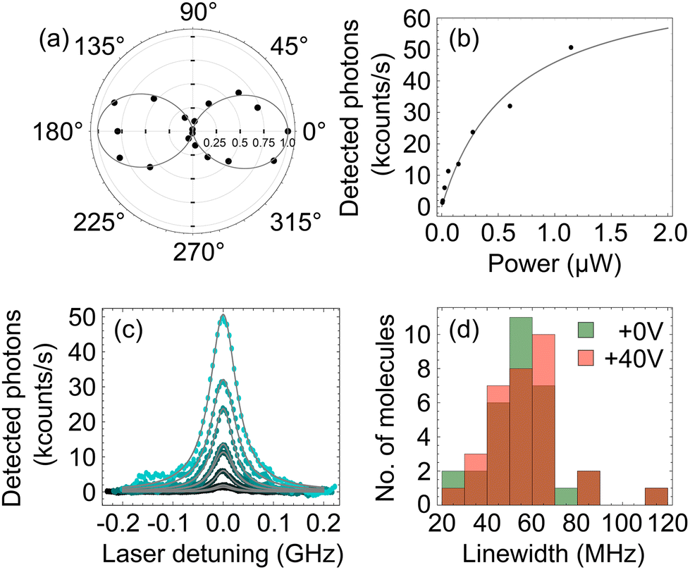 | ||
| Fig. 2 (a) Polar plot of the normalised counts, averaged from four different molecules as the polarisation of the excitation laser is varied, showing the expected response of the linear dipole of the molecule. A cos2 curve has been fitted to the data points. (b) Detected photons with increasing excitation power from a single molecule (data points) showing saturation behaviour according to eqn (3) (solid line). (c) The evolution of the fluorescence excitation spectrum of the molecule for different values of excitation power, showing power broadening of the line. (d) Histogram of the low-power linewidth of 32 identified molecules for two different values of the positive straining voltage, 0 V and +40 V, showing no significant change in the distribution. | ||
Next, we verified the presence of DBT molecules with a narrow ZPL linewidth. We optimised the collection for a bright spot on this map and scanned the laser wavelength from 783 nm to 783.1 nm to observe multiple peaks in the fluorescence excitation spectrum. Each Lorentzian peak in the spectrum corresponds to the excitation of the singlet S0,0 → S1,0 transition of a single molecule, and the subsequent collection of the red-shifted emission on S1,0 → S0,n>0 transition(s). The second label corresponds to the vibrational sub-level of the relevant singlet electronic state. The energy level diagram in Fig. 1(c) shows the excitation (green) and collected emission (red) transitions. A single molecule was selected with a central ZPL frequency of 382875.5 GHz and this process was repeated for increasing excitation power. The maximum fluorescence count rate of the molecule R saturated as is typical for a quantum emitter,40 shown in Fig. 2(b). This can be fitted with a saturation curve of the form
 | (3) |
3.2 Strain tuning measurement
We then proceeded to apply strain to the sample. We began by applying a positive voltage to the piezoelectric strip up to +60 V in steps of 5 V. For each voltage we scanned the excitation laser from 783.0 nm to 783.1 nm and collected the emitted photons. Fig. 3a shows the intensity of measured light from the sample as a function of laser detuning38 and applied voltage. The expected amount of strain (see section 2) for each voltage value is presented on the right side axis of the plot. Fig. 3b shows a zoom-in of a small frequency range, with fewer voltages, demonstrating the presence of Lorentzian features corresponding to individual molecules being excited. | ||
| Fig. 3 (a) Density plot of the intensity of collected light as a function of laser detuning38 and the applied positive voltage. The right axis of the plot shows the estimated strain for each voltage value, calculated from the expected strain per unit V for this piezoelectric device (see section 2). There is a clear linear frequency shift as the voltage increases. (b) Impact of the positive straining voltage on the fluorescence excitation spectrum across a sampled frequency window. Each red curve corresponds to the measured spectrum at a different applied voltage. There is a linear change of the position of the peaks towards smaller frequencies. (c) As in (b) but for the negative straining voltage. A similar linear displacement of the peaks can be seen here towards higher frequencies. (d) As in (b) but this time using the inactive sample. There is no steady change in the spectra of the emitters with voltage, which implies that the tuning seen in the previous cases occurred due to the applied strain. | ||
As the voltage increases we see a clear shift in the central frequency of the lines. Tracking individual molecules from 0 V to +60 V we find a linear red-shift in the molecular frequency with voltage. A histogram of tuning rates is presented in Fig. 4, where we see a Gaussian distribution centered at −10.57(3) MHz per V with a standard deviation of 0.56(3) MHz per V.
 | ||
| Fig. 4 Extracted tuning rates for the case of the positive voltage on the main sample, the negative voltage on the main sample and the positive voltage on the inactive sample. | ||
We repeated the measurement of the low-power linewidth through fitting Lorentzian functions to the frequency scans at a voltage of +40 V. Again, modelling as a Weibull distribution we find a mean linewidth of 56.5(6) MHz with a standard deviation of 17.7(8) MHz. A histogram of this data is shown in Fig. 2d. This is very similar to initial measurements, indicating that tuning through the application of strain does not introduce excess dephasing and would be suitable for applications requiring lifetime-limited photons.41–44
Next, we followed the same procedure only this time with negative voltage values, ranging from 0 V to −60 V. Since the negative voltage results in a bending of the strip in the opposite direction, the strain that is induced on the crystal is also oppositely directed. The detected detuning across a segment of the total number of emitters is shown in Fig. 3c. Similar to the positive voltage case, there is a linear shift of the spectral peaks, only this time towards higher frequencies (blue detuning). Again, through linear fitting we derived the tuning rates for this case as well and presented them in Fig. 4. We see a similar Gaussian distribution, with an average of 10.31(2) MHz per V and a standard deviation of 0.28(2) MHz per V. The two distributions are well overlapped demonstrating that reversing the sign of the voltage bias applies the opposite strain to the molecules.
As the measured tuning is linear with this voltage is strong evidence we are not observing Stark tuning;14 however, in order to fully rule out Stark tuning as a mechanism for this tuning effect, we replaced the sample with an inactive piezoelectric strip. We performed another positive voltage measurement in exactly the same way as before using this sample. In Fig. 3d we present a section of the corresponding emission spectrum for every voltage that we used. There is almost no change in the position of the spectral peaks, as expected, which is another strong indication that the tuning presented above is due to the strain that is applied to the crystal. This is more visible in Fig. 4 where the tuning rates are shown for this sample as well. This time, the mean value of the distribution is −0.41(3) MHz per V, two orders of magnitude lower than those in the previous sample, with a standard deviation of 0.38(3) MHz per V.
3.3 Simulated tuning
To overcome the limited precision of our DFT calculations (10−4 eV), which is much higher than the maximum observed tuning of 4 × 10⁻⁶ eV, we simulated the result of larger amounts of strain on the crystal to calculate the tuning rate. This effect should be the same in the small strain regime where our experimental measurements reside. By simulating the system under higher ambient pressure we were able to determine the amount of strain that occurs. Combining this with the corresponding tuning that is presented in the literature,21,23 we estimate that a strain step of 0.031% is large enough to resolve the case where the strain is applied along the crystal's b axis. Since, as we shall see, strain along the b axis results in a lower tuning rate compared to strain along the a axis, this step should be large enough for both cases. This is the strain step that we used to simulate strain tuning along both the a and b crystal axes.In Fig. 5d we present the change in the frequency derived from the simulations for 5 strain steps. The orange points correspond to straining along the crystal's a axis and the blue points to strain along its b axis. As with the above experiment, we see a linear relationship between the applied strain and frequency tuning. Fitting straight lines to this we find tuning rates of −84(4) GHz per 0.01% of strain along the a axis and −33(4) GHz per 0.01% of strain along the b axis. These results are comparable with previously published values of frequency tuning when changing the ambient pressure, estimated as 10 GHz per 0.01% strain.21,23 From the experimental positive voltage tuning rate from Fig. 4 we observed that 1 V causes a detuning of 10.57(3) MHz. From our simulations we found that this detuning can occur from a strain of 1.26(6) × 10−6% along the a axis. Therefore, we can estimate that we are introducing a strain of 1.26(6) × 10−6% per V applied to the piezo, which is the same order of magnitude as the expected strain of 2.81 × 10⁻⁶% per V for this device at cryogenic temperature (see section 2). The discrepancy could arise from the strain relief, from the effect of fixing the strip on the metallic holder, from changes in the mounting materials used when cooled to a low temperature, or from a combination of the above.
 | ||
| Fig. 5 (a)–(c) Projection of the 5 × 5 × 3 crystal cell that was used in our simulations on each of its a, b and c crystal axes. The DBT atoms are in the centre of the cell and are presented with grey colour. (d) Simulated detuning due to strain along the crystal's a (orange points) and b (blue points) axes and linear fittings in each of these cases (dashed grey lines). | ||
4 Conclusions
Single DBT molecules in Ac crystal hosts are promising single photon sources with many potential applications. In this work we demonstrated a strain mechanism to achieve dynamical tuning of these sources in a repeatable way, reaching average tuning rates of −10.6 MHz per V and −10.1 MHz per V for the positive and negative voltage regimes, respectively. In contrast to other tuning mechanisms which lead to quadratic tuning coefficients, like those based on the Stark effect, this tuning is linear, which allows both a red shift and a blue shift of the photon frequency. We have also developed a method of combining MD and DFT techniques to estimate the expected frequency shift with a relatively low computational cost. In the future, we will improve our setup to be able to apply strain with varying magnitudes and directions to further explore the molecular response to its environment. For instance, it has been shown that fabricating quantum dot emitters on top of lead magnesium niobate-lead titanate (PMN-PT) actuators can lead to large in plane strain fields of an order of ∼0.15% or higher, corresponding to a linear tuning range of ∼242 GHz.45–47 By attaching our crystals on such a substrate we could potentially achieve much higher degrees of strain tuning, which could hold promise for modifying the lifetime of molecular vibrations.48 Another step forward is to simulate the effect of strain along an abstract direction in relation to the crystal axes by numerically studying the diffusion of the strain field across the crystals. Finally, implementing a piezoelectric layer either on top or below integrated waveguide structures would enable differential tuning of separate molecules on the same chip using strain. One could also envisage creating integrated photonic devices in piezoelectric materials such as thin-film lithium niobate, which could then be functionalised with molecular crystals. Implementing strain tuning in integrated structures while retaining narrow emission linewidths would be an important step forward in the fabrication of commercial quantum emitters based on single molecules.Author contributions
K. D. M. and A. S. C. conceptualised the work. K. D. M., P. B., D. P. B., and R. C. S. grew the organic crystals. A. F. and R. A. H. mounted the samples and set up the cryogenic probe. A. F., R. A. H., K. D. M., and P. B. carried out the cryogenic measurements. A. F., R. C. S., and A. S. C. analysed the data. A. F. drafted the manuscript and all authors contributed to the final draft. A. S. C. acquired funding and supervised the project.Conflicts of interest
There are no conflicts to declare.Acknowledgements
We thank Jon Dyne and Dave Pitman for their expert mechanical workshop support. This work was supported by EPSRC (EP/P030130/1, EP/P01058X/1, EP/R044031/1, and EP/S023607/1), the Royal Society (UF160475), and the EraNET Cofund Initiative QuantERA under the European Union's Horizon 2020 Research and Innovation Programme, Grant No. 731473 (ORQUID Project).References
- R. W. Boyd, S. G. Lukishova and V. N. Zadkov, Quantum photonics: pioneering advances and emerging applications, Springer, 2019, vol. 217 Search PubMed.
- H.-K. Lo, M. Curty and B. Qi, Phys. Rev. Lett., 2012, 108, 130503 CrossRef PubMed.
- J. L. O'Brien, Science, 2007, 318, 1567–1570 CrossRef.
- C. Clear, R. C. Schofield, K. D. Major, J. Iles-Smith, A. S. Clark and D. P. S. McCutcheon, Phys. Rev. Lett., 2020, 124, 153602 CrossRef CAS.
- W. H. Hesselink and D. A. Wiersma, J. Chem. Phys., 1980, 73, 648–663 CrossRef CAS.
- N. R. Verhart, M. Müller and M. Orrit, ChemPhysChem, 2016, 17, 1524–1529 CrossRef CAS.
- R. C. Schofield, P. Burdekin, A. Fasoulakis, L. Devanz, D. P. Bogusz, R. A. Hoggarth, K. D. Major and A. S. Clark, ChemPhysChem, 2022, 23, e202100809 CAS.
- J.-B. Trebbia, H. Ruf, P. Tamarat and B. Lounis, Opt. Express, 2009, 17, 23986–23991 CrossRef CAS PubMed.
- A. A. L. Nicolet, C. Hofmann, M. A. Kol'chenko, B. Kozankiewicz and M. Orrit, ChemPhysChem, 2007, 8, 1215–1220 CrossRef CAS PubMed.
- K. D. Major, Y.-H. Lien, C. Polisseni, S. Grandi, K. W. Kho, A. S. Clark, J. Hwang and E. A. Hinds, Rev. Sci. Instrum., 2015, 86, 083106 CrossRef PubMed.
- S. Pazzagli, P. Lombardi, D. Martella, M. Colautti, B. Tiribilli, F. S. Cataliotti and C. Toninelli, ACS Nano, 2018, 12, 4295–4303 CrossRef CAS.
- R. C. Schofield, C. Clear, R. A. Hoggarth, K. D. Major, D. P. S. McCutcheon and A. S. Clark, Phys. Rev. Res., 2022, 4, 013037 CrossRef CAS.
- R. Duquennoy, M. Colautti, R. Emadi, P. Majumder, P. Lombardi and C. Toninelli, Optica, 2022, 9, 731–737 CrossRef CAS.
- K. G. Schädler, C. Ciancico, S. Pazzagli, P. Lombardi, A. Bachtold, C. Toninelli, A. Reserbat-Plantey and F. H. L. Koppens, Nano Lett., 2019, 19, 3789–3795 CrossRef.
- C. F. de las Casas, D. J. Christle, J. Ul Hassan, T. Ohshima, N. T. Son and D. D. Awschalom, Appl. Phys. Lett., 2017, 111, 262403 CrossRef.
- I. Gerhardt, G. Wrigge and V. Sandoghdar, Mol. Phys., 2009, 107, 1975–1979 CrossRef CAS.
- J. Zhang, Y. Huo, A. Rastelli, M. Zopf, B. Höfer, Y. Chen, F. Ding and O. G. Schmidt, Nano Lett., 2015, 15, 422–427 CrossRef CAS.
- J. Q. Grim, A. S. Bracker, M. Zalalutdinov, S. G. Carter, A. C. Kozen, M. Kim, C. S. Kim, J. T. Mlack, M. Yakes and B. Lee, et al. , Nat. Mater., 2019, 18, 963–969 CrossRef CAS PubMed.
- M. Croci, H. J. Müschenborn, F. Güttler, A. Renn and U. P. Wild, Chem. Phys. Lett., 1993, 212, 71–77 CrossRef CAS.
- U. P. Wild, M. Croci, F. Güttler, M. Pirotta and A. Renn, J. Lumin., 1994, 60–61, 1003–1007 CrossRef CAS.
- Y. Tian, P. Navarro and M. Orrit, Phys. Rev. Lett., 2014, 113, 135505 CrossRef PubMed.
- RS Pro Datasheet 285-784, M641 Piezoelectric Ceramic Bimorph Element, https://docs.rs-online.com/67b9/0900766b81582396.pdf.
- A. A. L. Nicolet, P. Bordat, C. Hofmann, M. A. Kol'chenko, B. Kozankiewicz, R. Brown and M. Orrit, ChemPhysChem, 2007, 8, 1929–1936 CrossRef CAS PubMed.
- N. L. Allinger, Y. H. Yuh and J. H. Lii, J. Am. Chem. Soc., 1989, 111, 8551–8566 CrossRef CAS.
- N. L. Allinger and J.-H. Lii, J. Comput. Chem., 1987, 8, 1146–1153 CrossRef CAS.
- J. H. Lii and N. L. Allinger, J. Am. Chem. Soc., 1989, 111, 8566–8575 CrossRef CAS.
- P. Grančič, R. Bylsma, H. Meekes and H. M. Cuppen, Cryst. Growth Des., 2015, 15, 1625–1633 CrossRef.
- P. Bordat and R. Brown, Chem. Phys. Lett., 2000, 331, 439–445 CrossRef CAS.
- P. Bordat and R. Brown, J. Chem. Phys., 2002, 116, 229–236 CrossRef CAS.
- D. Williams, J. Mol. Struct., 1999, 485–486, 321–347 CrossRef CAS.
- D. E. Williams, J. Chem. Phys., 1966, 45, 3770–3778 CrossRef CAS.
- A. D. Becke, J. Chem. Phys., 1993, 98, 1372–1377 CrossRef CAS.
- P. J. Stephens, F. J. Devlin, C. F. Chabalowski and M. J. Frisch, J. Phys. Chem., 1994, 98, 11623–11627 CrossRef CAS.
- F. Weigend and R. Ahlrichs, Phys. Chem. Chem. Phys., 2005, 7, 3297–3305 RSC.
- F. Neese, F. Wennmohs, A. Hansen and U. Becker, Chem. Phys., 2009, 356, 98–109 CrossRef CAS.
- F. Neese, Wiley Interdiscip. Rev.: Comput. Mol. Sci., 2012, 2, 73–78 CAS.
- F. Neese, Wiley Interdiscip. Rev.: Comput. Mol. Sci., 2018, 8, e1327 Search PubMed.
- The laser detuning is defined as νlaser − ν0 where νlaser is the laser frequency and ν0 is the fixed frequency from which the detuning is measured. In Fig. 3(a)ν0 = 382829.8 GHz, in Fig. 3(b)ν0 = 382866.8 GHz, in Fig. 3(c)ν0 = 382865.1 GHz, and in Fig. 3(d)ν0 = 382837.1 GHz.
- R. C. Schofield, K. D. Major, S. Grandi, S. Boissier, E. A. Hinds and A. S. Clark, J. Phys. Commun., 2018, 2, 115027 CrossRef CAS.
- S. Grandi, K. D. Major, C. Polisseni, S. Boissier, A. S. Clark and E. A. Hinds, Phys. Rev. A, 2016, 94, 063839 CrossRef.
- R. Bedington, J. M. Arrazola and A. Ling, npj Quantum Inf., 2017, 3, 1–13 CrossRef.
- C. Toninelli, I. Gerhardt, A. S. Clark, A. Reserbat-Plantey, S. Götzinger, Z. Ristanović, M. Colautti, P. Lombardi, K. D. Major and I. Deperasińska, et al. , Nat. Mater., 2021, 20, 1615–1628 CrossRef CAS PubMed.
- C. Liu, S. Zhang, L. Zhao, P. Chen, C. H. F. Fung, H. F. Chau, M. M. T. Loy and S. Du, Opt. Express, 2013, 21, 9505–9513 CrossRef PubMed.
- S. Wehner, D. Elkouss and R. Hanson, Science, 2018, 362, eaam9288 CrossRef.
- T. Zander, A. Herklotz, S. Kiravittaya, M. Benyoucef, F. Ding, P. Atkinson, S. Kumar, J. D. Plumhof, K. Dörr, A. Rastelli and O. G. Schmidt, Opt. Express, 2009, 17, 22452–22461 CrossRef CAS.
- S. Kumar, R. Trotta, E. Zallo, J. D. Plumhof, P. Atkinson, A. Rastelli and O. G. Schmidt, Appl. Phys. Lett., 2011, 99, 161118 CrossRef.
- R. Trotta, E. Zallo, E. Magerl, O. G. Schmidt and A. Rastelli, Phys. Rev. B: Condens. Matter Mater. Phys., 2013, 88, 155312 CrossRef.
- B. Gurlek, V. Sandoghdar and D. Martin-Cano, Phys. Rev. Lett., 2021, 127, 123603 CrossRef CAS.
| This journal is © The Royal Society of Chemistry 2023 |