DOI:
10.1039/D2NR06115E
(Paper)
Nanoscale, 2023,
15, 185-194
Suppressing interface recombination in CZTSSe solar cells by simple selenization with synchronous interface gradient doping†
Received
1st November 2022
, Accepted 25th November 2022
First published on 26th November 2022
Abstract
The main bottleneck in the development of kesterite Cu2ZnSn(S,Se)4 (CZTSSe) solar cells is their very low VOC due to severe carrier recombination. Specifically, due to the poor defect environment and unfavorable band structure, carrier recombination at the front interface is considered to be one of the most serious issues. Thus, to reduce the interface recombination and VOC deficit, we propose a convenient and effective strategy for Cd gradient doping near the front interface during selenization. The formed Cd gradient significantly reduced the CuZn defects and related [2CuZn + SnZn] defect clusters near the CZTSSe–CdS heterojunction, thus significantly suppressing the interface recombination near the heterojunction. Benefitting from the formed Cd gradient, a champion device with 12.14% PCE was achieved with the VOC significantly improved from 432 mV to 486 mV. The proposed element gradient doping strategy can offer a new idea for selenization and element gradient doping in other photoelectric devices.
1. Introduction
As a type of semiconductor material with excellent properties such as high abundance of constituent elements, low cost, high absorption coefficient (>104 cm−1) and adjustable band gap, Cu2ZnSnS(S,Se)4 (CZTSSe)-based solar cells have attracted significant attention.1–3 At present, the development of CZTSSe thin-film solar cells has made a new breakthrough, reaching a world-record efficiency of 13.6% (VOC = 537 mV).4 Nonetheless, there is still a large gap with the Shockley–Queisser (S–Q) limit efficiency,5,6 and it is also lagging behind silicon and other thin-film technologies. The main bottleneck of CZTSSe solar cells is considered to be their very low open-circuit voltage (VOC),1,7–9 which has only reached 65.5% of the S–Q limit VOC (820 mV). The large VOC loss of CZTSSe solar cells is closely related to their absorber and associated interfaces, at which carrier recombination is inevitable. According to the (Eg − Ea) vs. (Eg/q − Voc) diagram reported by Kumar et al.,10 the dominant carrier recombination in CZTSSe solar cells is interface recombination because its recombination activation energy is much lower than the band gap of the absorber. Among the different interfaces in CZTSSe solar cells, the CZTSSe/CdS heterojunction interface is particularly important for effective charge separation and collection. Also, it is the mail factor that causes severe VOC loss and limits the improvement in device performance.11
The poor defect environment at the CZTSSe/CdS heterojunction interface is one of the main factors causing the VOC deficit. Firstly, the formation of CuZn antisite defect near the heterojunction becomes smaller due to the upward shift of the Fermi level (EF). Thus, there is higher concentration of CuZn antisite defects than the bulk of the absorber, thus forming a large number of recombination centers. Secondly, a high concentration of p-type CuZn defects at the interface will lead to the pinning of Fermi level, causing only a small band bending in the absorber and limiting the extraction of charges.12,13 Thirdly, the formation energy of [2CuZn + SnZn] defect complexes will be reduced and begin to proliferate due to the presence of extensive Cu–Zn disorder. These defects are considered to induce severe carrier recombination, resulting in a VOC deficit and hindering the performance improvement of CZTSSe devices.14 Recently, numerous studies have been reported on improving the defect environment via the cation substitution (or doping) strategy. CuZn defects can be suppressed by partially substituting Cu with Ag15–17 and partially substituting Zn with Cd.18–20 Meanwhile, Sn-related deep defect centers can be eliminated by substituting Sn with Ge.21–23 Among the substitution or doping elements, Cd has receiving considerable attention and has been studied extensively in recent years. Conventional substitution or doping generally leads to a homogeneous distribution of Cd in the CZTSSe absorber. However, the high ratio substitution or doping of Cd will dramatically reduce the band gap of the CZTSSe absorber, limiting the further improvement in VOC. Moreover, uniform substitution or doping causes a flat conduction band structure, which is not conducive to the transport of photoinduced electrons to the front interface. Recently, Yi Zhang et al. reported the preparation of a band gap-graded CZTSSe absorber via heterojunction annealing.24 The formed Cd gradient and band gap gradient in the CZTSSe absorber not only dramatically improved the electrons transport but also reduced the carrier recombination at the front interface. Obviously, the construction of a suitable Cd gradient near the CZTSSe–CdS heterojunction not only can suppress a high concentration of CuZn in the CZTSSe absorber, but also can cause better band alignment between the CZTSSe absorber and CdS buffer layer. The partial substitution of Zn by Cd significantly reduces the CuZn anti-position defect near the front interface, alleviating Fermi level pinning and inhibiting the formation of the [2CuZn + SnZn] deep-level defect complex. The formed Cd gradient causes a gradually decrease in the conduction band minimum (CBM) towards the front side of the CZTSSe absorber, which is not only beneficial for photoinduced electron transport towards the front interface, but also optimizes the band arrangement of the CZTSSe/CdS heterojunction. Thus, this tailored band gap gradient can suppress interface recombination at the CZTSSe/CdS heterojunction, thus improving the efficiency of CZTSSe solar cells.
Herein, we propose a simple selenization method with synchronous Cd gradient doping in the CZTSSe absorber near the CZTSSe–CdS heterojunction. During the selenization process, a piece of soda-lime glass (SLG) covered with CdS film was place in close contact with the CZTSSe precursor film for Cd doping. At the selenization temperature, Cd gradually diffused into the formed CZTSSe absorber with a Cd gradient towards the front side of the CZTSSe absorber. The formed Cd gradient in the CZTSSe absorber near the CZTSSe–CdS heterojunction significantly reduced the CuZn anti-position defect near the CZTSSe–CdS heterojunction and interface recombination in the CZTSSe solar cells. Consequently, the efficiency of the CZTSSe solar cells improved from 10.16% to 12.14%, while the VOC improved from 432 mV to 486 mV.
2. Experimental
2.1. Chemicals and materials
Copper powder (10–30 nm, 99.9%) was purchased from Shanghai Macklin Biochemical Co., Ltd. Zinc powder (99.9%), tin powder (99%), sulfur powder (99.9%), selenium powder (99.9%), cadmium sulfate (CdSO4·8/3H2O, 99%), thiourea (NH2CSNH2, 99%) and ethanolamine (C2H7NO, 99.5%) were purchased from Shanghai Aladdin Biochemical Technology Co., Ltd. Ammonia solution (NH3·H2O, 25%) was obtained from Tianjin Fuyu Fine Chemical Co, Ltd. 2-Ethanedithiol (HSCH2CH2SH, 98%) and 1,2-ethylenediamine (H2NCH2CH2NH2, 99%) were purchased from Alfa Aesar. Thioglycolic acid (C2H4O2S, 98%) was purchased from Acros. All chemicals were used directly without further purification.
2.2. Preparation of CZTSSe precursor films
The CZTSSe precursor films were prepared via the spin-coating method according to our previous work.25
2.3. Preparation of CdS films
The CdS films were prepared via the chemical bath deposition (CBD) method. Firstly, 0.30 mmol CdSO4, 12.5 mL NH3·H2O and 1.50 mmol thiourea were added in turn to 250 mL deionized water in a 500 mL beaker and the mixture was stirred at room temperature until a clear solution was obtained. Then, pretreated SLG was vertically fixed onto a holder, which was placed in the middle of the beaker at the bottom. Finally, the beaker was placed in a water bath at 65 °C for the deposition of the CdS films. CdS films with different thicknesses were obtained after 8, 12 and 16 min deposition.
2.4. Selenization of CZTSSe precursor films and fabrication of solar cells
For Cd gradient doping, the CZTSSe precursor films were selenized upon close contact with the CdS film covered SLG. Firstly, SLG covered with a CdS film was placed in a square graphite box with the CdS film facing upward. Then, the CZTSSe precursor film was covered on the SLG covered with the CdS film, with the CZTSSe precursor film facing downward. Finally, the CZTSSe precursor films were selenized at 550 °C for 15 min in a nitrogen atmosphere and cooled to room temperature to obtain the Cd gradient-doped CZTSSe absorber. To prepare the reference CZTSSe absorber, the CZTSSe precursor film was only selenized upon close contact with a cleaned SLG. CZTSSe solar cells were fabricated based on the structure of MgF/Ag/ITO/i-ZnO/CdS/CZTSSe/Mo-SLG according to our previous work.25 The active area of the fabricated solar cells was 0.21 cm2.
2.5. Characterization
X-ray diffraction (XRD) patterns were obtained using an X-ray diffractometer (Bruker AXS, D8-Advance). The current density–voltage (J–V) curves were measured under standard illumination intensity (light intensity AM 1.5) using a solar simulator (Zolix, SS150) and Keithley 2400. The external quantum efficiency (EQE) was achieved using a Zolix SCS100 QE system equipped with a 150 W xenon light source, in the wavelength range of 300–1400 nm. XPS was performed using an X-ray photoelectron spectrometer (Thermo Fisher Scientific, ESCALAB 250Xi). The working voltage was 12.5 kV, the filament current was 16 mA, and the signal accumulation was carried out for 10 cycles. To detect the element information at different depths in the CZTSSe absorber, the sample was etched using an Ar ion beam at an etching rate of ∼0.25 nm s−1. The XPS binding energies were calibrated using the C 1s peak at 284.80 eV. The valence band potential of the CZTSSe absorber at different depths was determined via ultraviolet photoelectron spectroscopy (UPS) (Thermo Fisher Scientific, ESCALAB 250Xi). The capacitance–voltage (C–V) curves and J–V–T curves were obtained using a deep-level transient spectrometer (DLTS) system (FT-1030 HERA DLTS). The C–V data were obtained in the dark in the scan range of −1 to 0 V. The J–V–T data were collected in the range of 120 to 300 K at a step size of 10 K.
3. Results and discussion
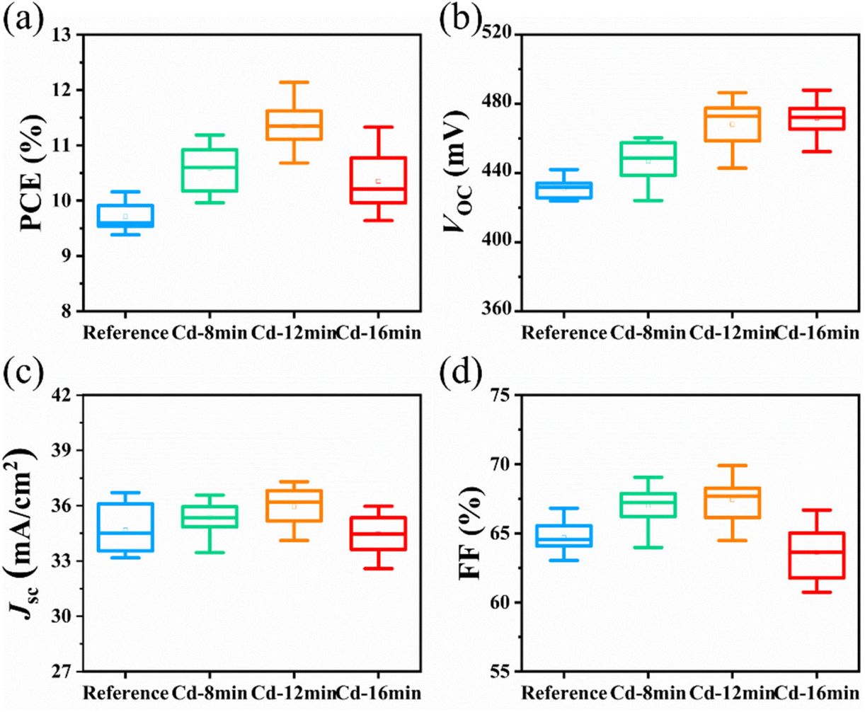
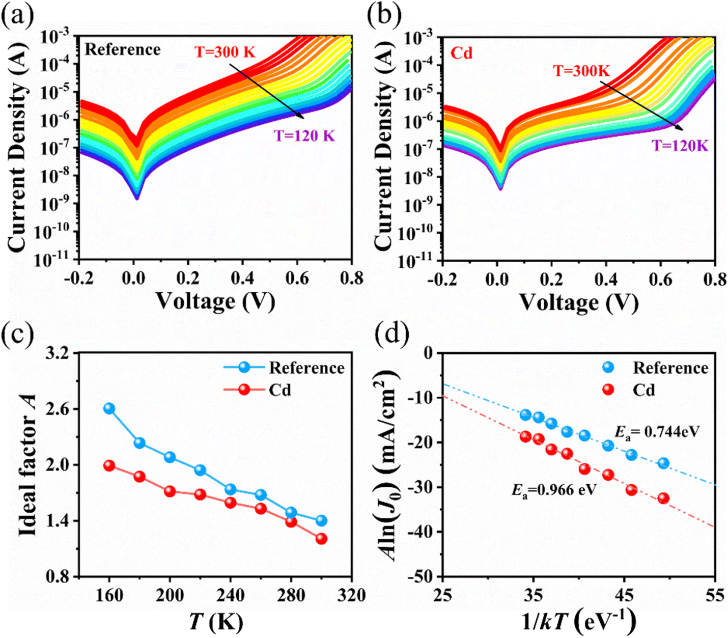
In this work, the CZTSSe precursor films were selenized at 550 °C for 15 min to obtain CZTSSe absorbers with a similar structure. Consequently, the thickness of the CdS films on SLG strongly affected the diffusion of Cd in the formed CZTSSe absorber during the selenization procedure, thus influencing the performance of the fabricated CZTSSe solar cells. In this work, CdS films with different thicknesses were obtained via CBD for 8, 12 and 16 min. As shown in Fig. 1, the thickness of the CdS films obviously affected the photovoltaic parameters of the fabricated CZTSSe solar cells. As the deposition time of the CdS films (or thickness of CdS films) increased, the open-circuit voltage (VOC) of the fabricated CZTSSe solar cells significantly improved. This improvement can be attributed to the reduction in the amount of defects and carrier recombination suppression caused by Cd doping in the formed CZTSSe absorber. However, when the deposition time was more than 12 min, the short-circuit current density (JSC) and fill factor (FF) decreased obviously, causing a decrease in the photoelectric conversion efficiency (PCE) of the fabricated CZTSSe solar cells. Excessive Cd doping significantly reduced the band gap near the CZTSSe/CdS heterojunction interface, which may have caused a reduction in the JSC and FF. Finally, the best conversion efficiency of 12.14% was obtained from the CdS film deposited for 12 min.
 |
| | Fig. 1 Photovoltaic parameters of CZTSSe solar cells fabricated from CZTSSe absorbers selenized with different CdS films. PCE (a); VOC (b); JSC (c) and FF (d). | |
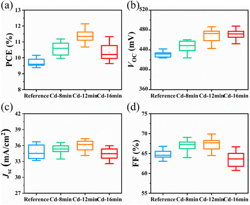
During the selenization procedure, the thickness of the CdS films on SLG can evidently affect the diffusion or doping of Cd into the formed CZTSSe absorber. Thus, to further evaluate the optimal diffusion depth and/or amount of Cd in the CZTSSe absorber, we performed detailed depth-profiling XPS measurements on the CZTSSe absorber selenized with CdS film deposited for 12 min (Cd-12 min). Generally, Cd is more likely to occupy the partial lattice of the same main group Zn. Thus, the high-resolution spectra of Zn 2p and Cd 3d at different depths in the CZTSSe absorber were measured, as shown in Fig. 2a and b, respectively. The spin orbital splitting peaks for Zn 2p were observed at 1044.6 eV (2p 1/2) and 1021.6 eV (2p 3/2) with a binding energy difference of 23.0 eV, corresponding to the oxidation state of Zn(II). The doublet peaks of Cd 3d, which split into 411.8 eV (3d 3/2) and 405.2 eV (3d 5/2) with the peak splitting of 6.6 eV, can be assigned to Cd(II). With an increase in the etching time, the intensity of the Cd 3d peaks decreased gradually, indicating a decrease in Cd content from the CZTSSe absorber surface to the interior. Meanwhile, the intensity of the Zn 2p peaks remained almost unchanged. By integrating the XPS peaks of Zn 2p and Cd 3d at different depths (etching time), the approximate contents of Zn and Cd could be obtained.15 The variation tendency of the Cd/(Cd + Zn) ratio at different depths is plotted in Fig. 2c. As shown, the Cd/(Cd + Zn) ratio in the CZTSSe absorber decreased quickly initially, and then slowly with an increase in the etching time. When the etching time reached 350s (etching depth ∼88 nm), the Cd/(Cd + Zn) ratio decreased from more than 15% (surface) to less than 3% (interior). Specifically, a Cd gradient near the front surface was achieved in the formed CZTSSe absorber. All these phenomena and results can be explained by the diffusion of the cadmium from CdS film to the CZTSSe absorber during the selenization process. Thus, we concluded that the optimal diffusion depth of Cd in the CZTSSe absorber should be less than 100 nm.
 |
| | Fig. 2 High-resolution XPS spectra for Zn 2p (a) and Cd 3d (b) at different etching depths (expressed in etching time); Cd/(Cd+Zn) ratio (c) at different etching depths (expressed in etching time). | |
It has been reported that the band gap of the CZTSSe absorber is linearly correlated with the Cd/(Cd + Zn) ratio. Thus, the band gap near the surface of the CZTSSe absorber may also show a gradient distribution with the Cd gradient, thus affecting the separation and collection of the photocarriers near the CZTSSe/CdS heterojunction. To validate the effect of Cd gradient doping on the band structure of the CZTSSe absorber and band matching with CdS at the heterojunction, UPS measurements were performed on the CZTSSe absorber with Cd gradient doping at different etching depths, CZTSSe absorber without Cd doping and CdS film. Fig. 3a shows the energy level difference between the Fermi energy level (EF) and the valence band maximum (VBM) of the CZTSSe absorber at different etching depths. As shown, the energy level difference between EF and the VBM decreased from 0.48 eV at the surface to 0.43 eV at the etching depth from 350 s etching time. Meanwhile, the energy level difference between EF and the VBM for the CZTSSe absorber without Cd doping and CdS was 0.38 and 1.68 eV, respectively. Specifically, the doping of Cd in the CZTSSe absorber will cause the p-type conductivity of the CZTSSe absorber to become weak. The Ecutoff can be obtained from the long-tail region of the UPS spectra, as shown in Fig. 3b. Subsequently, we can determine the EF of the different films according to the Ecutoff.26 As previously reported, there is a linear correlation between Eg of the CZTSSe absorber and Cd/(Cd + Zn) ratio, as follows:24,27Eg(x) = 1.085–0.462x, where x represents the Cd/(Cd + Zn) ratio. The Eg of the CZTSSe absorber with Cd gradient doping at different etching depths was calculated and shown in Table 1. The band gap of the CZTSSe absorber without Cd doping was obtained from the EQE curve (Fig. 4c). Based on the obtained data in Table 1, the conduction band minimum (CBM) and detailed band arrangement were obtained, as shown in Fig. 3c. With a decrease in the Cd doping amount from the surface to the bulk of the CZTSSe absorber, the CBM of the CZTSSe absorber increased from −4.29 eV to −4.21 eV, while the VBM increased from −5.31 eV to −5.28 eV, corresponding to an increase in the band gap from 1.02 eV to 1.07 eV. The conduction band position of the CZTSSe absorber is mainly determined by the hybrid orbital between Sn4+ and Se2− (S2−), while the valence band position is determined by the anti-bonding orbital between Se2− (S2−) and Cu+.28 The substitution of Zn by Cd with a larger atomic radius leads to lattice expansion, which increases the distance between Sn and Se (S) and weakens the bonding between Sn4+ and Se2− (S2−), thus making the conduction band position move down evidently, while the valence band position moves down slightly.28,29 A gradient descent in the CBM is favorable for electron transport to the forward interface, and thus beneficial for an improvement in the device performance. In addition, the conduction band offset (CBO) between CdS and the CZTSSe absorber is another key factor affecting the carrier transport and recombination at the CZTSSe/CdS heterojunction interface. After Cd gradient doping, the CBO value increased from 0.12 eV to 0.24 eV, which is close to the theoretical optimal CBO value of 0.25 eV.30 Therefore, suitable Cd gradient doping is conducive to reducing the carrier recombination at the CZTSSe/CdS heterojunction interface.31 With a further increase in Cd doping near the surface of the CZTSSe absorber, a larger “spike” barrier can be formed, which will reduce the performance of the fabricated device.30
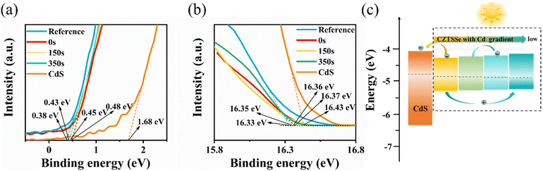 |
| | Fig. 3 UPS spectra of CZTSSe absorber with Cd gradient doping (a) and (b) and schematic diagram of band structure at the CZTSSe/CdS heterojunction interface (c). | |
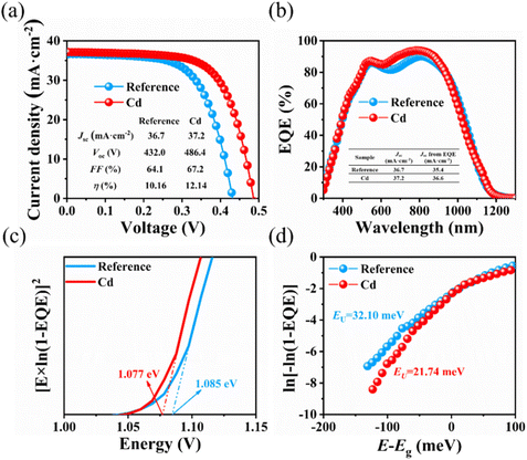 |
| | Fig. 4
J–V (a) and EQE curves (b) of CZTSSe solar cells with/without Cd gradient doping. Eg derived from EQE curves (c) and ln[−ln[1 − EQE]] vs. E − Eg curves obtained from EQE curves (d). | |
Table 1
E
g, EF, VBM and CBM of the CZTSSe absorber with Cd gradient doping at different etching depths
| Etching time (s) |
E
g (eV) |
VBM (eV) |
W
F (eV) |
E
F (eV) |
CBM (eV) |
| 0 |
1.02 |
−5.31 |
0.48 |
−4.83 |
−4.29 |
| 150 |
1.05 |
−5.29 |
0.45 |
−4.84 |
−4.24 |
| 350 |
1.07 |
−5.28 |
0.43 |
−4.85 |
−4.21 |
| CZTSSe (without Cd) |
1.08 |
−5.25 |
0.38 |
−4.87 |
−4.17 |
| CdS |
2.40 |
−6.45 |
1.68 |
−4.77 |
−4.05 |
The J–V curves of the CZTSSe devices with/without Cd gradient doping are shown in Fig. 4a and the detailed PV parameters derived from the J–V curves are shown in Table 2 and Fig. S2.† After optimal Cd gradient doping, the PCE of the fabricated CZTSSe solar cells increased from 10.16% to 12.14% with an increase in the VOC from 432.0 mV to 486.4 mV, showing a remarkable improvement. The EQE spectrum was used to study the effect of Cd gradient doping on the spectral response of the fabricated CZTSSe devices. As shown in Fig. 4b, the CZTSSe devices with/without Cd gradient doping showed a similar spectral response in the short wavelength region (300–500 nm), indicating the same absorption originating from the CdS/i-ZnO/ITO layers. In the wavelength region of 500 nm–900 nm, a slight of spectral response enhancement was observed for the CZTSSe device with Cd gradient doping. This enhancement can be attributed to the improvement in the CZTSSe absorber quality near the surface and p–n junction quality. In addition, a slight reduction in the band gap (calculated from EQE curve and shown in Fig. 4c) was observed for the CZTSSe device with Cd gradient doping, which led to slight expansion of the spectral absorption. This slight spectral response enhancement is consistent with the increase of Jsc from CZTSSe device with Cd gradient doping. In the case of the CZTSSe solar cells, a high VOC deficit is generally accompanied with severe band tailing and large Urbach energy.32 Urbach band-tail analysis (Fig. 4d) was conducted to calculate the band-tailing for the CZTSSe absorbers with/without Cd gradient doping and the Urbach energy (EU) was extracted from the reciprocal of d(ln[−ln[1 − EQE]])/d(E − Eg).25,33 As shown, the EU of the CZTSSe device decreased from 32.10 mV to 21.74 mV after optimal Cd gradient doping, indicating that Cd gradient doping can effectively relieve the band tailing of the CZTSSe absorber and enhance the VOC.
Table 2 Detailed PV parameters of CZTSSe solar cells with and without Cd gradient doping
| Sample |
PCE (%) |
V
OC (mV) |
J
SC (mA cm−2) |
FF (%) |
R
s (Ω cm2) |
R
sh (Ω cm2) |
G
sh (mS cm−2) |
J
0 (mA cm−2) |
A
|
| Reference |
10.16 |
432.0 |
36.7 |
64.1 |
0.85 |
508.25 |
1.96 |
1.01 × 10⁻³ |
1.82 |
| With Cd |
12.14 |
486.4 |
37.2 |
67.2 |
0.54 |
603.22 |
1.65 |
3.86 × 10⁻⁴ |
1.69 |
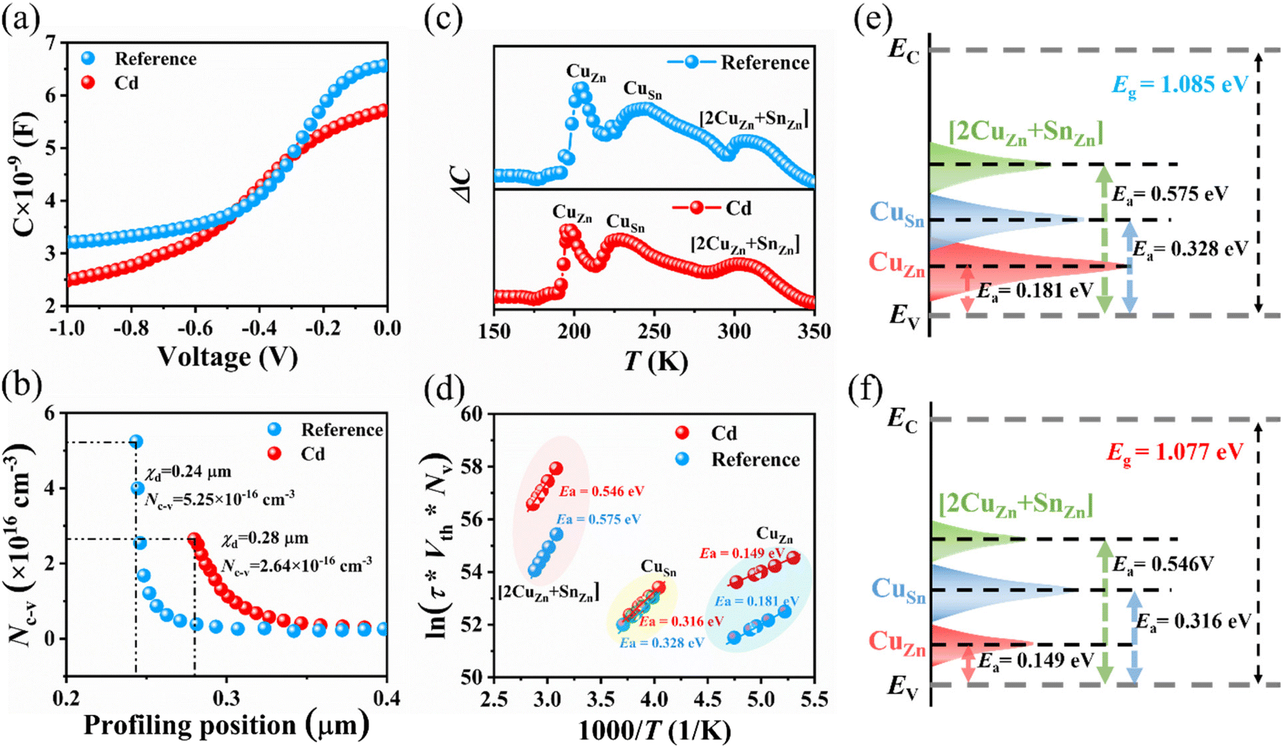
Capacitance–voltage (C–V) was used to analyze the depletion width (Wd) and free carrier concentration (Ncv) of the CZTSSe devices with/without Cd gradient doping (Fig. 5a). The Wd and Ncv were obtained using the following equations:34
| |  | (1) |
| |  | (2) |
where
ε0,
ε,
A,
C and
q represent the vacuum dielectric constant of solar cells (8.85 × 10
−12 F m
−1), dielectric constant of CZTSSe (8.6), active area (0.21 cm
2), device capacitance and electron charge (1.60 × 10
−19 C), respectively. As shown in
Fig. 5b, the
Wd of the CZTSSe device increased from 0.24 μm to 0.28 μm after Cd gradient doping, implying better carrier separation and collection efficiency. After Cd gradient doping,
NCV decreased from 5.25 × 10
−16 cm
−3 to 2.64 × 10
−16 cm
−3. The
NCV of the CZTSSe device is mainly derived from Cu
Zn defects, and thus the reduction in
NCV may be due to the effective passivation of the Cu
Zn defects by the doped Cd. To gain deep insights into the spatial defect environment evolution after Cd gradient doping, capacitance-mode deep-level transient spectroscopy (C-DLTS) was performed in the dark in the temperature range of 120 K–350 K. The reverse bias voltage (
VR), pulse voltage (
VP) and pulse width were set to be −0.4 V, 0.4 V and 3 ms, respectively. The DLTS spectra of the CZTSSe solar cells with/without Cd gradient doping are shown in
Fig. 5c. As shown, three characteristic peaks were detected (located at around 200 K, 260 K and 310 K), indicating that three types of defects exist in both CZTSSe devices. Arrhenius curves (
Fig. 5d) were used to identify the defect type and concentration in the two CZTSSe devices according to the following equation:
34| |  | (3) |
where
τ is the emission time constant,
Vth is the thermal rate of the carrier,
Nv is the effective density state of the carrier,
Xp is the entropy factor of the carrier,
σp is the capture cross section of the carrier,
Ea is the defect activation energy,
Ev is the valence band energy level,
k is the Boltzmann constant and
T is the temperature. The
Ea can be obtained from the slope of the Arrhenius curve, which represents the distance between the defect energy level and valence band maximum. The defect concentration (
NT) can be calculated according to the following equation:
34| |  | (4) |
where
NS is the concentration of shallow defects, Δ
C is the amplitude of the capacitance transients, and
CR is the capacitance at equilibrium reverse bias. According first-principles calculations,
Ea in the range of 0.12–0.20 eV, 0.22–0.40 eV and 0.52–0.64 eV can be ascribed to Cu
Zn defects, Cu
Sn defects and [2Cu
Zn + Sn
Zn] defect clusters, respectively.
35,36 The
Ea and
NT calculated for the Cu
Zn defects, Cu
Sn defects and [2Cu
Zn + Sn
Zn] defect clusters are shown in
Table 3 and
Fig. 5e, f. After Cd gradient doping, the
Ea of Cu
Zn defects decreased from 0.181 eV to 0.149 eV, while
NT declined from 6.01 × 10
14 cm
−3 to 4.29 × 10
13 cm
−3. Specifically, Cd gradient doping significantly inhibited the Cu
Zn defects near the depletion region, which reduced the carrier recombination and alleviated the Fermi energy pinning at the CZTSSe/CdS heterojunction interface.
12 Also, the Cu
Zn-related defect cluster [2Cu
Zn + Sn
Zn] was suppressed significantly by the proposed Cd gradient doping. The [2Cu
Zn + Sn
Zn] defect cluster is considered to be responsible for the band-tailing, and thus it is understandable that Cd gradient doping can effectively suppress the formation of the band-tailing, consistent with its relatively smaller
EU.
37 On the contrary, the
Ea and
NT of Cu
Sn defect did not change much, indicating that Cd gradient doping cannot effectively inhibit the formation of Cu
Sn defects.
 |
| | Fig. 5
C–V curves (a). Depletion width (Wd) and free carrier concentration (Ncv) obtained from C–V curves (b). DLTS spectra (c). Arrhenius curves obtained from DLTS spectra (d). Elementary diagram of diverse spatial distribution of defects for CZTSSe solar cells before (e) and after Cd gradient doping (f). | |
Table 3 Activation energy (Ea) and concentration (NT) of different defects in the CZTSSe solar cells
| Sample |
Activation energy Ea (eV) |
Trap concentration NT (cm−3) |
Possible defect level |
| Reference |
0.575 |
7.73 × 10¹³ |
[2CuZn + SnZn] |
| 0.328 |
1.84 × 10¹⁴ |
CuSn |
| 0.181 |
6.01 × 10¹⁴ |
CuZn |
| |
| With Cd |
0.546 |
3.96 × 10¹³ |
[2CuZn + SnZn] |
| 0.316 |
1.06 × 10¹⁴ |
CuSn |
| 0.149 |
4.29 × 10¹³ |
CuZn |
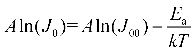
The temperature–dependent current density–voltage (J–V–T) curves of the CZTSSe devices with/without Cd gradient doping were used to investigate the charge carrier transport mechanism at the interface.15,38–40Fig. 6a and b present the J–V–T curves of the CZTSSe devices with/without Cd gradient doping in the range of 120 K–300 K. The J–V–T curve of the CZTSSe device with Cd gradient doping showed weak diode characteristic, while that of the CZTSSe device without Cd gradient doping remained benign diode characteristic, indicating that the transmission barrier decreased due to Cd gradient doping.40 The ideal factor A of the CZTSSe device with/without Cd gradient doping at different temperatures was extracted from the J–V–T curve, as shown in Fig. 6c. With an increase in temperature, the A of the CZTSSe devices decreased significantly, indicating a negative correlation between A and temperature. Compared to the reference device, the A values of the CZTSSe device with Cd gradient doping were lower and showed a lower temperature dependence, revealing that the Shockley–Read–Hall recombination dominated in the depletion region.41,42 In contrast, the A values of the CZTSSe device without Cd gradient doping were larger and showed a stronger temperature dependence, indicating that tunneling enhanced recombination dominated. We believe that Cd gradient doping can improve the heterojunction quality and inhibit the interface recombination, which will contribute to the promotion of the device performance. Ulteriorly, the linear relationship between A![[thin space (1/6-em)]](https://www.rsc.org/images/entities/char_2009.gif) ln(J0) and 1/kT was plotted to determine the recombination path in the different CZTSSe devices according the following equation:
ln(J0) and 1/kT was plotted to determine the recombination path in the different CZTSSe devices according the following equation:
| |  | (5) |
where
J0,
J00,
A,
k,
T and
Ea represent the reverse saturation current density, pre-factor dependent on the recombination path, ideal factor, Boltzmann constant, temperature and carrier recombination activation energy, respectively.
Ea can be obtained from the slope of the fitted linear regression between
Aln(
J0) and 1/
kT. By comparing the calculated
Ea value with band gap (
Eg) value of the CZTSSe devices, the main recombination path can be determined. If the
Ea value is close to the
Eg value, bulk recombination is dominant in the device. Alternatively, if the
Ea value is much less than the
Eg value, interface recombination is considered to be dominant.
38,40 As shown in
Fig. 6d, the
Ea for the CZTSSe device without Cd gradient doping was calculated to be 0.744 eV, which is much smaller than its
Eg (1.085 eV), indicating the presence of the interface recombination path in the CZTSSe device. Meanwhile, the
Ea for CZTSSe device with Cd gradient doping was calculated to be 0.966 eV, which is close to its
Eg (1.077 eV), indicating the presence of the bulk recombination path in the CZTSSe device. This result suggests that the interface recombination was significantly suppressed by the proposed Cd gradient doping.
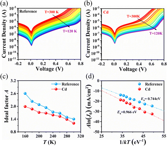 |
| | Fig. 6 Temperature–dependent dark current density–voltage curves of CZTSSe device with/without Cd gradient doping (a) and (b). Ideal factor A at different temperatures extracted from the J–V–T curves (c). Aln(J0) versus 1/kT plot of CZTSSe device with/without Cd gradient doping (d). | |
The band structure analysis, defect environment and recombination path all confirmed the contribution of Cd gradient doping to the suppression of interface recombination at the CZTSSe/CdS heterojunction. Furthermore, electrochemical impedance spectroscopy (EIS) was used to analyze the carrier recombination process. The Nyquist plots of the CZTSSe device with/without Cd gradient doping are shown in Fig. S3.† The interface recombination resistance (RCT) can be obtained from the diameter of the Nyquist plots, while the carrier lifetime (τ) can be calculated from the equation τ = Rct × Cj (Cj = capacitance).41,43 The calculated results are listed in Table 4. After Cd gradient doping, RCT increased from 54.8 Ω to 111.7 Ω, while τ was prolonged from 2.67 μs to 5.18 μs. These improvements proved that interface recombination was significantly suppressed by the proposed Cd gradient doping.
Table 4
R
CT and τ calculated from the Nyquist plots of the CZTSSe device with/without Cd gradient doping
| Solar cells |
R
ct (Ω) |
C
j (nF) |
τ (μs) |
| Reference |
54.8 |
48.8 |
2.67 |
| With Cd |
111.7 |
46.4 |
5.18 |
4. Conclusions
In summary, a Cd gradient near the front surface was achieved in the CZTSSe absorber via the optimized selenization process. The formed Cd gradient and gradient band structure near the CZTSSe–CdS heterojunction were validated by XPS and UPS depth profile analysis. The formed Cd gradient significantly reduced the CuZn defect and related [2CuZn + SnZn] defect cluster near the CZTSSe–CdS heterojunction, thus significantly suppressing the interface recombination near the heterojunction. Further characterization and measurement confirmed the suppression of interface recombination by the proposed Cd gradient doping, contributing to the alleviation of the VOC deficit. Finally, a champion device with 12.14% PEC was achieved, with the VOC significantly improved from 432 mV to 486 mV. In conclusion, this study provides a convenient and effective method to achieve element gradient doping, which contributes to interface recombination suppression and device performance improvement. It is expected that our findings may inspire the use of the selenization process and element gradient doping in other photoelectric devices.
Conflicts of interest
The authors declare no conflicts of interests.
Acknowledgements
This work was supported by the National Natural Science Foundation of China (61874159, 61974173, 62074052 and 62104061), the Joint Talent Cultivation Funds of NSFC-HN (U1904192) and the Science and Technology Innovation Talents in Universities of Henan Province (18HASTIT016 and 21HASTIT023).
References
- S. Giraldo, Z. Jehl, M. Placidi, V. Izquierdo-Roca, A. Perez-Rodriguez and E. Saucedo, Adv. Mater., 2019, 31, 1806692 CrossRef.
- W. Wang, M. T. Winkler, O. Gunawan, T. Gokmen, T. K. Todorov, Y. Zhu and D. B. Mitzi, Adv. Energy Mater., 2014, 4, 1301465 CrossRef.
- D.-H. Son, S.-H. Kim, S.-Y. Kim, Y.-I. Kim, J.-H. Sim, S.-N. Park, D.-H. Jeon, D.-K. Hwang, S.-J. Sung, J.-K. Kang, K.-J. Yang and D.-H. Kim, J. Mater. Chem. A, 2019, 7, 25279–25289 RSC.
- M. A. Green, E. D. Dunlop, J. Hohl-Ebinger, M. Yoshita, N. Kopidakis, K. Bothe, D. Hinken, M. Rauer and X. Hao, Prog. Photovoltaics, 2022, 30, 687–701 Search PubMed.
- S. Kim, J. A. Márquez, T. Unold and A. Walsh, Energy Environ. Sci., 2020, 13, 1481–1491 RSC.
- W. Shockley and H. J. Queisser, J. Appl. Phys., 1961, 32, 510–519 CrossRef CAS.
- D. Shin, B. Saparov and D. B. Mitzi, Adv. Energy Mater., 2017, 7, 1602366 CrossRef.
- F. Liu, S. Wu, Y. Zhang, X. Hao and L. Ding, Sci. Bull., 2020, 65, 698–701 CrossRef CAS.
- F. Liu, Q. Zeng, J. Li, X. Hao, A. Ho-Baillie, J. Tang and M. A. Green, Mater. Today, 2020, 41, 120–142 CrossRef CAS.
- N. Nln, K. Kaur and M. Kumar, J. Mater. Chem. A, 2020, 8, 21547–21584 RSC.
- K. Kaur, N. Kumar and M. Kumar, J. Mater. Chem. A, 2017, 5, 3069–3090 RSC.
- Z.-K. Yuan, S. Chen, H. Xiang, X.-G. Gong, A. Walsh, J.-S. Park, I. Repins and S.-H. Wei, Adv. Funct. Mater., 2015, 25, 6733–6743 CrossRef CAS.
- K. B. Cheon, S. K. Hwang, S. W. Seo, J. H. Park, M. A. Park and J. Y. Kim, ACS Appl. Mater. Interfaces, 2019, 11, 24088–24095 CrossRef CAS.
- W. Chen, D. Dahliah, G.-M. Rignanese and G. Hautier, Energy Environ. Sci., 2021, 14, 3567–3578 RSC.
- C. Cui, D. Kou, W. Zhou, Z. Zhou, S. Yuan, Y. Qi, Z. Zheng and S. Wu, J. Energy Chem., 2022, 67, 555–562 CrossRef CAS.
- J. Fu, D. Kou, W. Zhou, Z. Zhou, S. Yuan, Y. Qi and S. Wu, J. Mater. Chem. A, 2020, 8, 22292–22301 RSC.
- Y. Qi, Y. Liu, D. Kou, W. Zhou, Z. Zhou, Q. Tian, S. Yuan, Y. Meng and S. Wu, ACS Appl. Mater. Interfaces, 2020, 12, 14213–14223 CrossRef CAS PubMed.
- J. Fu, Q. Tian, Z. Zhou, D. Kou, Y. Meng, W. Zhou and S. Wu, Chem. Mater., 2016, 28, 5821–5828 CrossRef CAS.
- Z. Su, G. Liang, P. Fan, J. Luo, Z. Zheng, Z. Xie, W. Wang, S. Chen, J. Hu, Y. Wei, C. Yan, J. Huang, X. Hao and F. Liu, Adv. Mater., 2020, 32, 2000121 CrossRef CAS PubMed.
- C. Yan, K. Sun, J. Huang, S. Johnston, F. Liu, B. P. Veettil, K. Sun, A. Pu, F. Zhou, J. A. Stride, M. A. Green and X. Hao, ACS Energy Lett., 2017, 2, 930–936 CrossRef CAS.
- Y. Deng, Z. Zhou, X. Zhang, L. Cao, W. Zhou, D. Kou, Y. Qi, S. Yuan, Z. Zheng and S. Wu, J. Energy Chem., 2021, 61, 1–7 CrossRef CAS.
- A. D. Collord and H. W. Hillhouse, Chem. Mater., 2016, 28, 2067–2073 CrossRef CAS.
- W. Zhao, D. Pan and S. F. Liu, Nanoscale, 2016, 8, 10160–10165 RSC.
- H. Guo, R. Meng, G. Wang, S. Wang, L. Wu, J. Li, Z. Wang, J. Dong, X. Hao and Y. Zhang, Energy Environ. Sci., 2022, 15, 693–704 RSC.
- H.-Q. Xiao, W.-H. Zhou, D.-X. Kou, Z.-J. Zhou, Y.-N. Meng, Y.-F. Qi, S.-J. Yuan, Q.-W. Tian and S.-X. Wu, Green Chem., 2020, 22, 3597–3607 RSC.
- P. Dong, E. A. Fisher, M. V. Meli and S. Trudel, Nanoscale, 2020, 12, 19797–19803 RSC.
- Y.-F. Li, Z.-Y. Xiao, B. Yao, R. Deng, Z.-H. Ding, T. Wu, G. Yang, C.-R. Li, Z.-Y. Dong, L. Liu, L.-G. Zhang and H.-F. Zhao, J. Appl. Phys., 2013, 114, 183506 CrossRef.
- S. Chen, A. Walsh, Y. Luo, J.-H. Yang, X. G. Gong and S.-H. Wei, Phys. Rev. B: Condens. Matter Mater. Phys., 2010, 82, 195203 CrossRef.
- Z. Su, J. M. R. Tan, X. Li, X. Zeng, S. K. Batabyal and L. H. Wong, Adv. Energy Mater., 2015, 5, 1500682 CrossRef.
- K. Sun, C. Yan, F. Liu, J. Huang, F. Zhou, J. A. Stride, M. Green and X. Hao, Adv. Energy Mater., 2016, 6, 1600046 CrossRef.
- J. Lee, T. Enkhbat, G. Han, M. H. Sharif, E. Enkhbayar, H. Yoo, J. H. Kim, S. Kim and J. Kim, Nano Energy, 2020, 78, 105206 CrossRef CAS.
- S. Ma, H. Li, J. Hong, H. Wang, X. Lu, Y. Chen, L. Sun, F. Yue, J. W. Tomm, J. Chu and S. Chen, J. Phys. Chem. Lett., 2019, 10, 7929–7936 CrossRef CAS PubMed.
- Y. Du, S. Wang, Q. Tian, Y. Zhao, X. Chang, H. Xiao, Y. Deng, S. Chen, S. Wu and S. Liu, Adv. Funct. Mater., 2021, 31, 2010325 CrossRef CAS.
-
D. Abou-Ras, T. Kirchartz and U. Rau, Advanced Characterization Techniques for Thin Film Solar Cells, Wiley, 2011 Search PubMed.
- S. Chen, A. Walsh, X. G. Gong and S. H. Wei, Adv. Mater., 2013, 25, 1522–1539 CrossRef CAS.
- S. Das, S. K. Chaudhuri, R. N. Bhattacharya and K. C. Mandal, Appl. Phys. Lett., 2014, 104, 192106 CrossRef.
- J. Wang, J. Zhou, X. Xu, F. Meng, C. Xiang, L. Lou, K. Yin, B. Duan, H. Wu, J. Shi, Y. Luo, D. Li, H. Xin and Q. Meng, Adv. Mater., 2022, 34, 2202858 CrossRef CAS.
- G. S. Park, V. B. Chu, B. W. Kim, D. W. Kim, H. S. Oh, Y. J. Hwang and B. K. Min, ACS Appl. Mater. Interfaces, 2018, 10, 9894–9899 CrossRef CAS.
- F. Werner, M. H. Wolter, S. Siebentritt, G. Sozzi, S. Di Napoli, R. Menozzi, P. Jackson, W. Witte, R. Carron, E. Avancini, T. P. Weiss and S. Buecheler, Prog. Photovoltaics, 2018, 26, 911–923 CAS.
- Y. Zhao, S. Yuan, Q. Chang, Z. Zhou, D. Kou, W. Zhou, Y. Qi and S. Wu, Adv. Funct. Mater., 2021, 31, 2007928 CrossRef CAS.
- J. Fu, Q. Tian, Y. Du, Q. Chang, Y. Guo, S. Yuan, Z. Zheng, S. Wu and S. Liu, Sol. RRL, 2022, 6, 2101032 CrossRef CAS.
- U. Rau, Appl. Phys. Lett., 1999, 74, 111 CrossRef CAS.
- S. K. Hwang, J. H. Park, K. B. Cheon, S. W. Seo, J. E. Song, I. J. Park, S. G. Ji, M. A. Park and J. Y. Kim, Prog. Photovoltaics, 2020, 28, 1345–1354 CAS.
|
| This journal is © The Royal Society of Chemistry 2023 |
Click here to see how this site uses Cookies. View our privacy policy here. 
 *,
Dong-Xing
Kou
*,
Dong-Xing
Kou