
 Open Access Article
 This Open Access Article is licensed under a Creative Commons Attribution-Non Commercial 3.0 Unported Licence
Synthesis of mono- and few-layered n-type WSe2 from solid state inorganic precursors†
Mauro
Och
a,
Konstantinos
Anastasiou
 c,
Ioannis
Leontis
c,
Giulia Zoe
Zemignani
af,
Pawel
Palczynski
a,
Ali
Mostaed
d,
Maria S.
Sokolikova
a,
Evgeny M.
Alexeev
e,
Haoyu
Bai
a,
Alexander I.
Tartakovskii
e,
Johannes
Lischner
ab,
Peter D.
Nellist
d,
Saverio
Russo
c and
Cecilia
Mattevi
*a
c,
Ioannis
Leontis
c,
Giulia Zoe
Zemignani
af,
Pawel
Palczynski
a,
Ali
Mostaed
d,
Maria S.
Sokolikova
a,
Evgeny M.
Alexeev
e,
Haoyu
Bai
a,
Alexander I.
Tartakovskii
e,
Johannes
Lischner
ab,
Peter D.
Nellist
d,
Saverio
Russo
c and
Cecilia
Mattevi
*a
aDepartment of Materials, Imperial College London, London, SW7 2AZ, UK. E-mail: c.mattevi@imperial.ac.uk
bThomas Young Centre for Theory and Simulation of Materials, Imperial College London, London, SW7 2AZ, UK
cDepartment of Physics and Astronomy, University of Exeter, Exeter, EX4 4QL, UK
dDepartment of Materials, University of Oxford, Oxford, OX1 3PH, UK
eDepartment of Physics and Astronomy, University of Sheffield, Sheffield, S3 7RH, UK
fCenter for Nano Science and Technology, Milan, Italy
First published on 12th September 2022
Abstract
Tuning the charge transport properties of two-dimensional transition metal dichalcogenides (TMDs) is pivotal to their future device integration in post-silicon technologies. To date, co-doping of TMDs during growth still proves to be challenging, and the synthesis of doped WSe2, an otherwise ambipolar material, has been mainly limited to p-doping. Here, we demonstrate the synthesis of high-quality n-type monolayered WSe2 flakes using a solid-state precursor for Se, zinc selenide. n-Type transport has been reported with prime electron mobilities of up to 10 cm2 V−1 s−1. We also demonstrate the tuneability of doping to p-type transport with hole mobilities of 50 cm2 V−1 s−1 after annealing in air. n-Doping has been attributed to the presence of Zn adatoms on the WSe2 flakes as revealed by X-ray photoelectron spectroscopy (XPS), spatially resolved time of flight secondary ion mass spectroscopy (SIMS) and angular dark-field scanning transmission electron microscopy (AD-STEM) characterization of WSe2 flakes. Monolayer WSe2 flakes exhibit a sharp photoluminescence (PL) peak at room temperature and highly uniform emission across the entire flake area, indicating a high degree of crystallinity of the material. This work provides new insight into the synthesis of TMDs with charge carrier control, to pave the way towards post-silicon electronics.
1 Introduction
The large family of TMDs has attracted increasing interest in the last decade due to their unique optical, electrical and catalytic properties.1,2 Monolayer WSe2 features a direct optical bandgap close to the near infra-red region (1.65 eV),3,4 possesses one of the highest charge carrier mobilities among TMDs5 and exhibits robust valley- and spin-splitting.6 In addition to the thermodynamically stable hexagonal 2H crystal phase, WSe2 can be stabilised in the distorted trigonal 1T’ phase too, which behaves as a 2D topological insulator,7 and it has also been reported to be an active catalyst for the electrocatalytic hydrogen evolution reaction.8 Promising applications of 2H-WSe2 have been reported in the areas of photovoltaics,9,10 spintronics,11,12 and optoelectronics.13–16 Additionally, WSe2 along with other TMDs are emerging as potentially transformative materials for ultra-short channel field-effect transistors (FETs) as the charge carriers are confined within the layer and their concentration is controlled by the gate voltage.17,18Chemical vapor deposition (CVD) is the most promising technique for the growth of high-quality crystals over a wafer scale on an industrial scale,19,20 as already demonstrated for III–V semiconductors. To date, monolayer WSe2 has been synthesized in the form of isolated flakes by CVD,21,22 and large-scale continuous films using metal–organic CVD (MOCVD).23 While CVD relies on the reaction between WO3 and Se powders in the presence of H2,24,25 MOCVD syntheses typically use highly volatile W(CO)6 and H2Se.26 The use of conspicuous amounts of H2 has been proven to be essential to enable the growth of WSe2 from Se powder27 as it acts as a reducing agent, increasing the reactivity of both the metal and the chalcogen precursors. This is because the W–Se bonding energy is higher than the one of W–S, therefore selenium is less reactive than sulphur in the growth of WX2.28,29 However, handling and storing H2 can present safety concerns, as it is highly flammable, while H2Se is extremely toxic even at low exposure concentrations.
Additionally, to fully implement WSe2 in a metal–oxide semiconductor (MOS)FET architecture and complementary metal oxide semiconductor (CMOS) logic, controlling the charge carrier type and density is of paramount importance.30,31 WSe2 is often reported as ambipolar or p-type, while n-type WSe2 has been rarely reported.31–35 Whilst p-doping of monolayer WSe2 has been achieved via CVD,36,37 stable n-doped WSe2 has been mainly demonstrated in bulk crystals grown via chemical vapor transport which then have to be exfoliated down to atomically thin layers.38
Here, we demonstrate the synthesis of high quality monolayer WSe2 with n-type transport using an inorganic compound (ZnSe) as the selenium precursor, without the use of either H2 or gaseous H2Se. The obtained triangular monolayered flakes extend over tens of micrometres in lateral size, and they exhibit n-type transport. Our synthesis approach relies on the use of ZnSe, which contains Se in a −2 oxidation state and facilitates the reactivity with W precursors, enabling the synthesis of WSe2 without the aid of H2 as the reducing agent. The material exhibits electron mobilities up to 10 cm2 V−1 s−1 extracted from the transfer curves of fabricated FETs as a result of their interaction with Zn adatoms. Upon annealing in air, the material displays p-type transport with hole mobilities up to 50 cm2 V−1 s−1 thus further confirming the high crystal quality. The material possesses high intrinsic crystalline quality, as demonstrated by the narrow linewidth of the room temperature PL, while the low temperature emission is dominated by localized emitters.
2 Results and discussion
The growth is performed in a single-zone tubular furnace sublimating a 50 wt% mixture of H2WO4–NaCl along with ZnSe powder, loaded in two different alumina crucibles and placed next to each other, heated to 825–850 °C at a low pressure (0.1–1 mbar) using argon as the carrier gas, as depicted in Fig. 1a. The target substrate for WSe2 synthesis is SiO2/Si as this is inexpensive and technologically relevant for future scalability. It was usually placed downstream next to the precursors and subjected to the same temperature. SiO2/Si substrates proved to give the best results in terms of thickness control, crystal size and homogeneity compared to sapphire and h-BN in our system (Fig. SI1a and b†).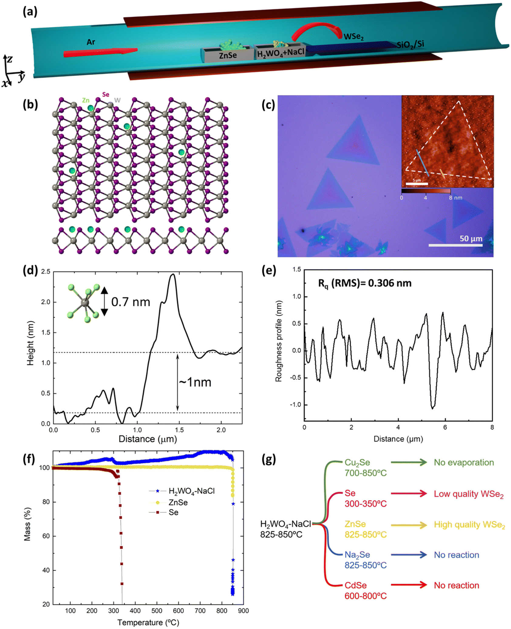 | ||
| Fig. 1 (a) Schematic of the WSe2 CVD growth process. (b) Ball and stick schematic of Zn-surface doped 2H-WSe2. (c) Optical micrograph of CVD grown monolayer Zn-surface doped WSe2 alongside the thickness measured by AFM. Inset: AFM map of a monolayer flake. (d) AFM step height profile of the flake. (e) Surface roughness of the WSe2 flake measured by AFM across the profile highlighted in blue colour in panel (c). (f) TGA analysis of CVD precursors performed at 0.1 mbar, which corresponds to the reactor pressure. The apparent mass gain in H2WO4 + NaCl most likely derives from a reaction with the crucible. (g) Diagram summarizing the different Se precursors used in this study with the relative evaporation temperatures and outcomes. | ||
In Fig. 1c, an optical micrograph of WSe2 monolayers with lateral sizes ranging from 10 up to ∼50 μm grown at 825 °C is reported. The average size of the grown triangles is ∼20 μm, in line with the reported sizes of the majority of CVD grown monolayers.39–41 Larger and thicker flakes were obtained by increasing the temperature of the synthesis to 850 °C (Fig. SI1c†). Moreover, the regular shape of the triangles suggests the absence of secondary ZnSe-rich phase growth. At growth temperatures lower than 800 °C, no reaction occurred and only amorphous round formations were present on the substrate, which were not Raman active (Fig. SI1d†). The atomic force microscopy (AFM) profile of typical WSe2 triangles shows a step height between the substrate and the flake of ∼1 nm (Fig. 1(d)), which is the expected height of a monolayer on a rough substrate such as silica.21,24 The roughness (Fig. 1e) is in line with the roughness normally measured for CVD grown TMDs42–46 and Rq(RMS) = 0.306 ± 0.264 nm and Ra = 0.265 ± 0.145 nm. In order to optimise the evaporation temperature of the precursors, we performed thermogravimetric analysis (TGA) under vacuum, as reported in Fig. 1f. ZnSe and H2WO4–NaCl abruptly sublimate at 850 °C and the W precursor sublimation profile matches the TGA data already reported in the literature.47 We also noticed that only around 30% of ZnSe loaded in the crucible actually evaporates; however, this is enough to enable the growth of WSe2 over mm2 areas.
The critical role played by the new Se precursor, introduced in our synthesis approach, can be understood using different Se-containing inorganic precursors. Substituting ZnSe with the more conventional Se powder, heated at 300–350 °C (evaporation temperature measured via vacuum TGA) in a separate furnace module, we obtained small WSe2 flakes (∼5 μm) with irregular shapes and various thicknesses (Fig. SI2a†). Without a reducing atmosphere, Se powder proved not to be reactive enough to promote the growth of WSe2, confirming the previous results.27 We tried to increase the Se supply in the system, loading Se powder along with ZnSe, but this deteriorated the crystal quality leading to polycrystalline films with irregular grain shapes and thicknesses (Fig. SI2b†). Other inorganic compounds were tested, such as Cu2Se and CdSe, but none of them led to any WSe2 growth using evaporation temperatures ranging from 700 to 850 °C. We found that Cu2Se was difficult to evaporate and the Se supply might have not been sufficient to enable the growth of crystals. In contrast, CdSe is more volatile than ZnSe, but the molecules were only transported and not dissociated as evidenced by bright red CdSe deposited in the downstream part of the quartz tube, resulting in bubble-like, metal-rich depositions (Fig. SI2c†). In the case of ZnSe-based growth, the downstream part of the tube was covered with green ZnSe, while the further downstream part was dark red due to the presence of Se. We then selected Na2Se to assess whether a compound with greater ionic character would be more efficient than ZnSe as a chalcogen precursor. However, the low volatility and reactivity of Na2Se were not sufficient to promote the WSe2 growth and only very few flakes were synthesized after several attempts (Fig. SI2d†). These results are schematically summarized in Fig. 1g.
The chemical composition of the as-grown material was characterised using XPS (Fig. 2(a–c)). The 4f core level doublet of W bound to Se can be found at 32.7 eV and 35.8 eV, as expected for WSe2.21,48 A small component from W–O binding appears as an additional doublet at 36.2 eV and 38.5 eV, respectively, and the contribution from the W 5p3/2 core level is present at 38.1 eV. For the 3d core levels of Se, the peak can be deconvoluted into two levels characteristic of Se bound to W: these are the Se 3d5/2 (54.9 eV) and Se 3d3/2 (55.8 eV) core levels. Additionally, we can detect the Zn presence at the impurity level looking at the 2p core level doublet at 1022.5 eV and 1045.5 eV, which are positions that correspond to the Zn2+ oxidation state.49 In Fig. SI3a,† we report the complete XPS survey spectrum highlighting all the core levels and Se Auger lines.
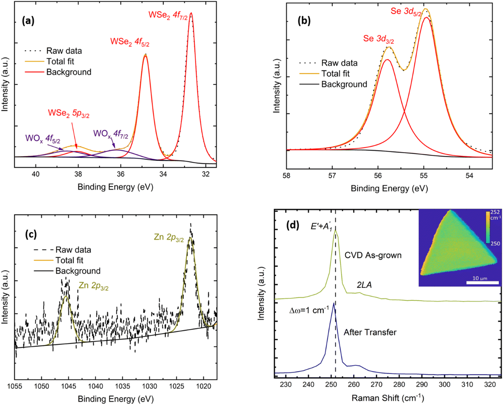 | ||
| Fig. 2 XPS spectra reporting the individual core level spectra of W 4f (a), Se 3d (b) and Zn 2p (c). (d) Typical Raman spectrum of the as-grown WSe2 monolayer and after PMMA-transfer on target SiO2. The principal E′ + A′1 and 2LA peaks are indicated alongside their change after transfer. Inset: map of the E′ + A′1 peak position of the CVD grown WSe2 monolayer. | ||
We further utilized Raman spectroscopy as a fast and non-destructive technique to gain additional information about the WSe2 crystal quality and thickness. A representative Raman spectrum recorded using 532 nm excitation wavelength is presented in Fig. 2d. The dominant peak at 251.8 cm−1 is the result of the convolution of the first order E′ in-plane and A′1 out-of-plane vibrational modes, while the weaker second-order 2LA(M) mode is visible at 261.8 cm−1, as expected for single-layer WSe2.50–52 The absence of the B12g mode at 310 cm−1 confirms the monolayer nature of the flake.50,51 The E′ + A′1 peak position does not significantly vary across the monolayer crystal, as shown in the map reported as the inset of Fig. 2d, suggesting that no visible defects or secondary phases are present. Recording the Raman spectrum of a WSe2 monolayer after a PMMA-mediated wet transfer onto a heavily doped SiO2/Si substrate used for FET fabrication, we can observe a red shift of 1 cm−1 in the positions of both vibrational modes. The change of the Raman mode frequencies indicates the release of compressive strain53 created during the growth due to the mismatch of the thermal expansion coefficients of WSe2 and the underlying SiO2 substrate, which causes different amounts of shrinkages during the cooling down phase of the CVD process.
In order to accurately detect the possible presence of Zn adatoms on the WSe2 flakes, we performed spatially resolved time of flight secondary ion mass spectroscopy (ToF-SIMS). This is a surface sensitive, fast analysis technique that enables the collection of high resolution mass spectra over large areas and within the sample, resulting in compositional maps and depth profiles. Compositional maps over areas larger than 100 × 100 μm2 were collected with a Bi+ gun on an as-grown sample, whereas to record the depth profiles we alternated the Bi+ analysing gun with a Cs+ gun, to remove the material after each measurement. We collected the elemental maps in both positive and negative ion channels and measured the distribution of W, Se and Zn (including abundant isotopes) over several flakes. In Fig. 3(a and b), we report the distribution of negative Se and Zn ions across an area of 100 × 100 μm2. These maps are generated by adding the mass spectra of the abundant isotopes shown in Fig. 3c, measured in the negative channel. The results arising from the positive channel are reported in Fig. SI4;† however, due to the extremely low positive ionisation of Se and Zn, we can see that the flake shapes are visible only in the W map. Remarkably, the Zn signal spatial distribution matches the Se one, demonstrating that the majority of Zn is present on the flakes rather than the SiO2 substrate. Additionally, the depth profile (Fig. 3d) clearly shows that the Zn atoms are distributed homogeneously throughout all the layers and do not form a secondary phase in the material, since the 64Zn peak intensity reflects the 80Se profile while etching through the flake. This suggests the preferential presence of Zn on the WSe2 material.
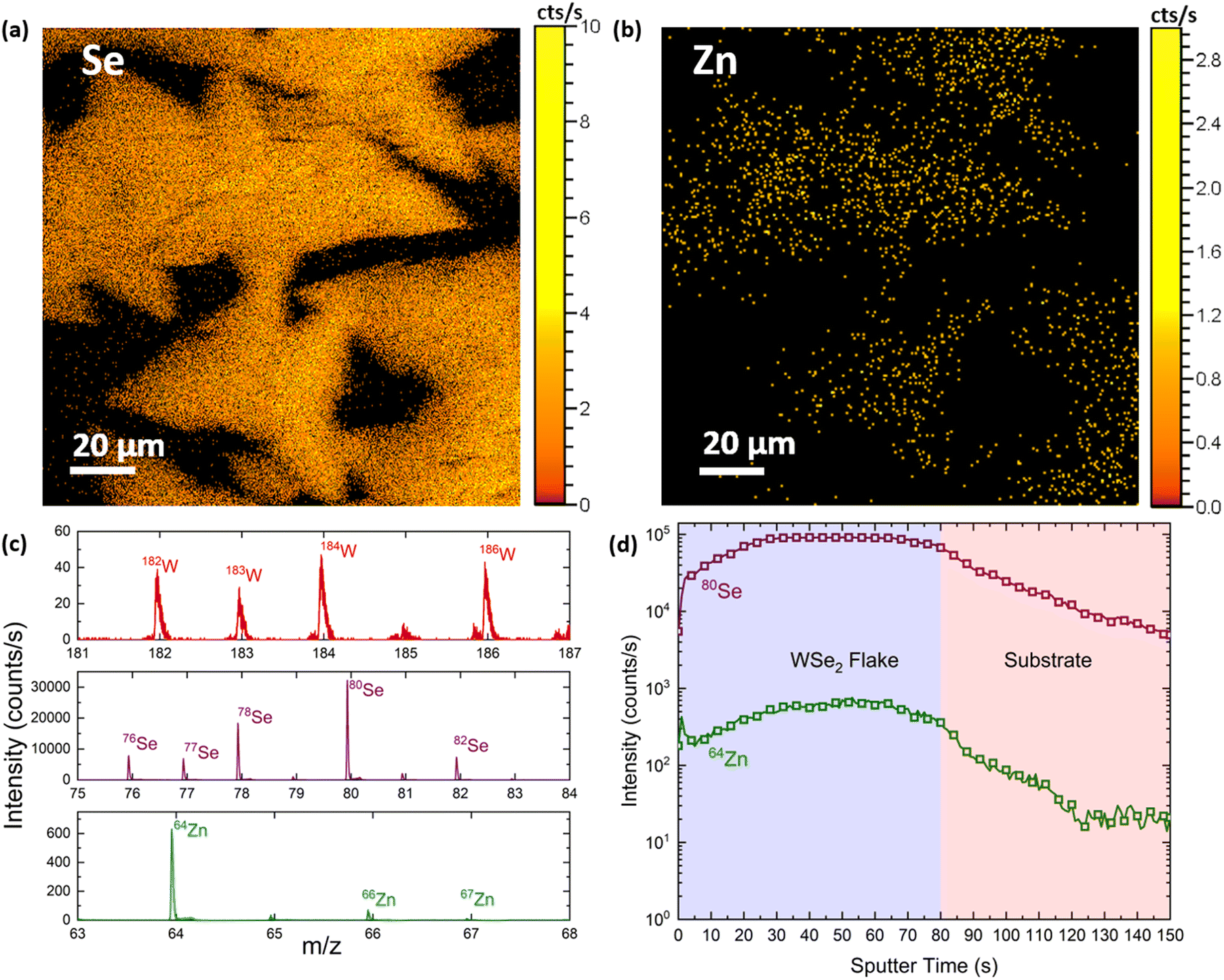 | ||
| Fig. 3 ToF-SIMS negative channel characterization of WSe2: (a) spatial distribution of the 76Se, 77Se, 78Se, 80Se and 82Se isotopes measured on multiple multilayer WSe2 flakes. (b) Distribution of the 64Zn, 66Zn and 67Zn isotopes. (c) Individual mass spectra of negative W, Se and Zn ions. m/z is the mass to charge ratio. (d) 80Se and 64Zn depth profiles against the sputter time. The blue region reports the profile of the actual flake, whereas after 80 seconds the Wse2 triangle is almost completely etched. | ||
To see more closely where the Zn atoms might be presented on WSe2, we have imaged the materials using angular dark-field (ADF) scanning transmission electron microscopy (STEM) as shown in Fig. 4. We can see the highly crystalline hexagonal structure of 2H-WSe2 (Fig. 4a) and white circles (Fig. 4a and b) highlighting a brighter contrast which suggests the presence of Zn adatoms on W atoms. This implies that Zn may act as a surface dopant, inducing n-type transport.15,54
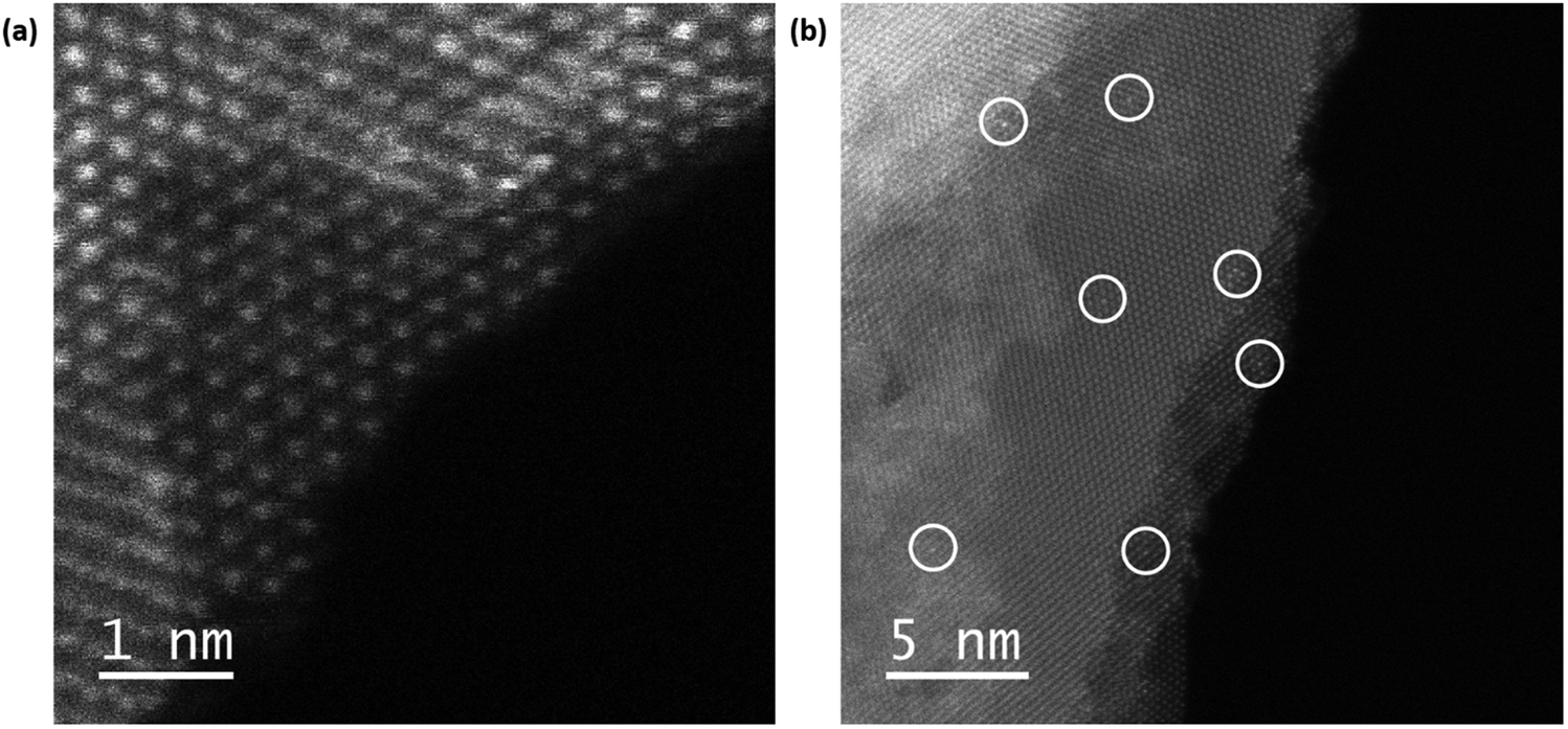 | ||
| Fig. 4 Atomic scale ADF-STEM characterization of multilayered WSe2. (a) Micrograph of a monolayer portion of the WSe2 flake where brighter spots suggest the presence of adatoms and (b) larger view of the distribution of adatoms on the WSe2 plane. | ||
We have studied the PL of the as-grown monolayer WSe2 at room and low temperature. The PL spectrum recorded at room temperature (Fig. 5a) shows the emission typical of high-quality monolayer crystals: the main PL peak at 1.65 eV corresponds to the radiative recombination of a neutral exciton, while a weaker lower-energy shoulder at 1.63 eV originates from charged exciton (trion) recombination. The former peak has a full width at half maximum (FWHM) of 53 meV, which is in agreement with the state-of-the-art values reported for CVD-grown WSe2 (Fig. 5c) by Chen et al.55 and Li et al.21 and is comparable to an exfoliated monolayer deposited onto SiO2.4 In order to investigate the homogeneity of our CVD grown material, we have acquired spatial mapping of PL.56 A typical PL image of one of the triangular crystals is shown in Fig. 5b. The PL intensity demonstrates excellent uniformity across the entire area of the crystal and does not show irregular patterns as reported in other studies.24,57 In other crystals, we observed quenching of PL along the lines connecting the centre of the triangle and its corners (Fig. SI3b†), originating from strain-induced bandgap variation.58Fig. 5d compares the PL and reflectance contrast (RC) spectra recorded at T = 10 K. While the RC spectrum shows a strong reflectance peak corresponding to the neutral exciton absorption, the PL spectrum is dominated by a lower energy emission band originating from defect-bound exciton recombination. The intensity of the localised emitter band is substantially reduced at T = 100 K and becomes negligibly low at T ≥ 160 K (Fig. SI3c†). The observed discrepancy between the narrow emission linewidth at room temperature and the apparent lower optical quality of the sample observed in low temperature measurements is likely a result of the strong interaction with the underlying SiO2 substrate. The intrinsic optical quality of the sample could be accessed by separating it from the substrate and encapsulating it in h-BN, as has been previously demonstrated for CVD-grown MoS2![[thin space (1/6-em)]](https://www.rsc.org/images/entities/char_2009.gif) 59 and WSe2.60
59 and WSe2.60
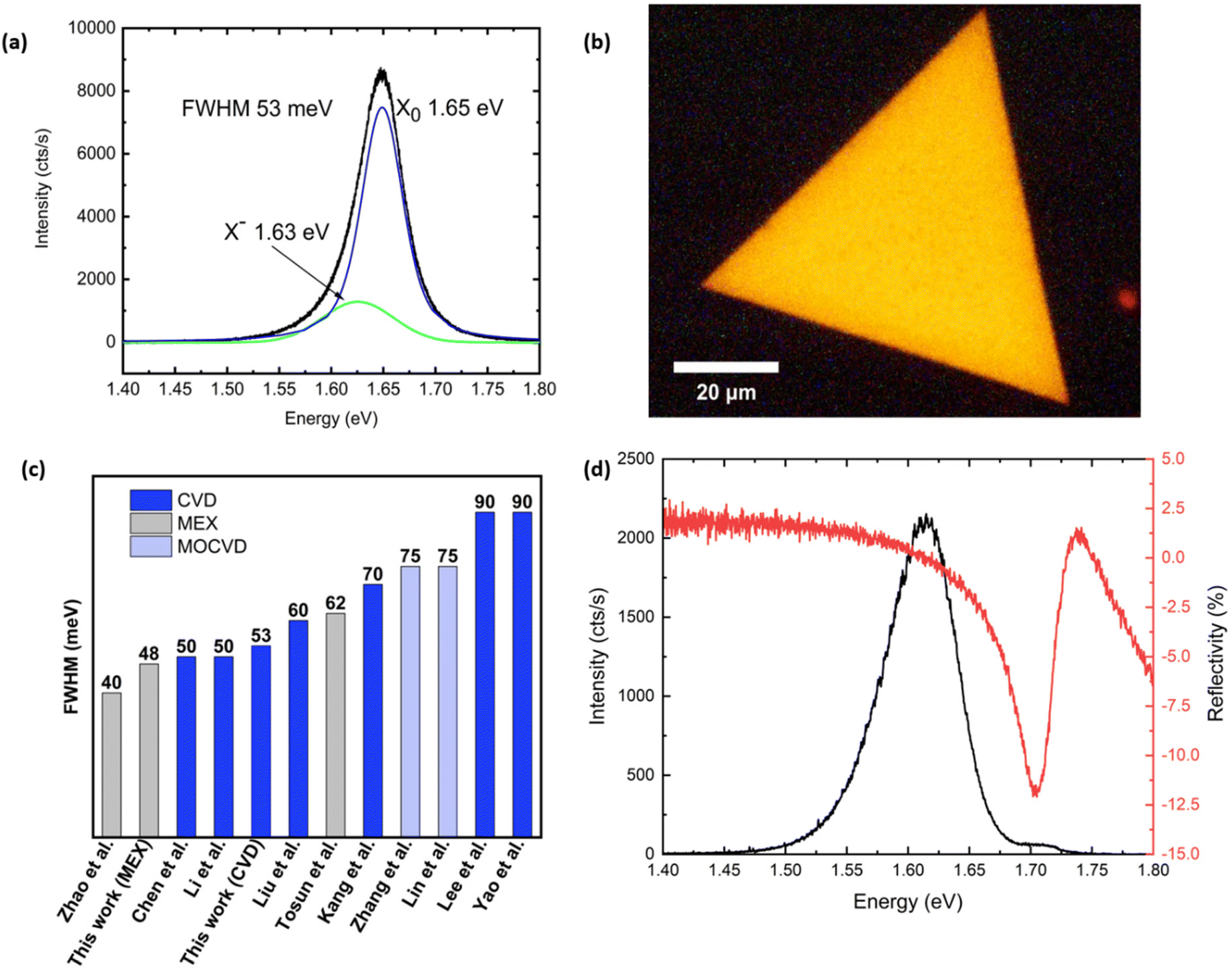 | ||
| Fig. 5 (a) Photoluminescence spectrum of monolayer WSe2 recorded at T = 297 K. (b) PL image of a WSe2 monolayer flake showing a highly uniform emission intensity across the entire area of the crystal. (c) Comparison chart of the measured FWHM tentative values extrapolated from the reported spectra in the literature and our value.4,21,24,26,55,57,90,91 We also report our measurement for an exfoliated flake. (d) PL (black) and RC (red) spectra of monolayer WSe2 recorded at T = 10 K. | ||
To ascertain the electrical transport properties of the CVD grown WSe2, we fabricated FETs with Ti/Au contacts. The devices were characterized in a vacuum (1 × 10⁻⁵ mbar) prior to and after multiple annealing steps, aimed at reducing unwanted contamination of the system incurred during the fabrication process. Fig. 6a shows the transfer characteristics of a representative device before and after different annealing conditions. Such a comparative plot shows a change of conductive charge types from electrons (before annealing and after vacuum annealing) to holes after air annealing. At the same time, the source–drain current increases upon annealing, attaining an ON/OFF ratio of ∼105, and the charge carrier mobility increases, reaching values as large as 10 cm2 V−1 s−1 (vacuum annealing) and 50 cm2 V−1 s−1 (annealing in air), see Fig. 6b. These values favourably compared to those reported in the literature of CVD grown WSe2 which can show both n- and p-type behaviour61–65 (Table S1 in the ESI†). The change of the carrier type is consistent with previous studies on annealing of WSe2 in the presence of oxygen, reporting an increase in hole doping due to the substitution of Se with O.66–69 To confirm the free carrier type and concentration, we have characterised the back gate dependence of the Hall coefficient using a 4-terminal Hall bar configuration in a number of as-grown WSe2 samples, using a constant current bias of 16 μA and perpendicular magnetic field −2T ≤ B ≤ 2T, as shown in the inset of Fig. 6c. These measurements confirm an average intrinsic n-type doping charge density nHall > 5 × 10¹⁵ m−2 at the back gate threshold voltage, whereas no valence band conduction is observed. This suggests that Zn adatoms act as surface n-dopants of WSe2. N-type doping is consistent with the work function of Zn being much larger than WSe2.15 Furthermore, the free carrier density increases linearly with the back-gate voltage following the expected functional dependence of the Drude conductivity. Finally, we characterized the spectral response of the photoresponsivity of the WSe2 transistor under a source–drain bias of Vsd = 1 V and with a gate bias of Vbg = −50 V (Fig. 6d). We observed a maximum of photoresponsivity at 610 nm, corresponding to an energy gap of E ∼ 2 eV, which is in agreement with the theoretical values predicted from the Mott–Wannier exciton model for monolayer WSe2 on a SiO2 substrate.70
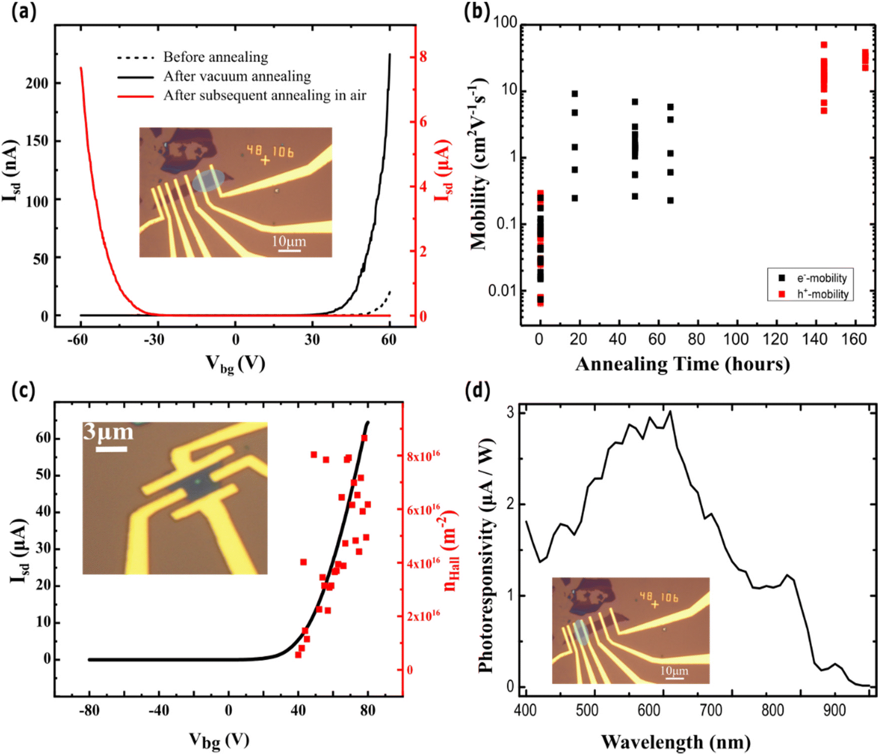 | ||
| Fig. 6 Optoelectronic characterization of a WSe2 FET: (a) transfer curves of the WSe2 FET (inset) under a source–drain bias of Vsd = 1 V (before, after an initial vacuum annealing step and after annealing in ambient air). (b) Effect of annealing on the mobility of both devices. (c) Transconductance (black, Vsd = 2 V) and gate-dependent Hall free carrier density (red data) measured for a representative Zn-surface doped Hall bar device (inset). (d) Spectral response of the device under a source and gate bias of Vsd = 3 V and Vbg = −50 V, respectively. | ||
3 Discussion
A possible explanation for the unique behaviour of ZnSe can be found by calculating its free energy in the gas phase. The standard enthalpy of formation ΔfH° of ZnSe(g) and the standard entropy ΔS° are reported to be 239 kJ mol−1 and 71.94 J K−1 mol−1, respectively.71 We can calculate the free energy (ΔG = ΔfH° − TΔS°) at 825 °C, corresponding to the ZnSe evaporation temperature, as 160 kJ mol−1. The free energy of Se2(g), which is the predominant Se species in the gas phase, is much lower and corresponds to −83 kJ mol−1.71 A higher reactant free energy lowers the total free energy variation of the process (ΔGprod − ΔGreact) and consequently produces larger driving force for the crystal growth reaction. This difference in free energy suggests that ZnSe is a more reactive precursor than molecular selenium.We propose the following chemical reactions to occur in our system:
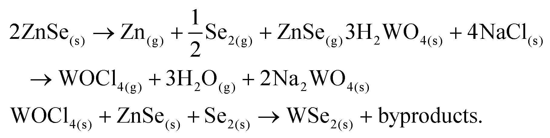
The first reaction is the partial dissociation of ZnSe at high temperature in the gas phase72 into metallic zinc and molecular selenium. The presence of green ZnSe on the downstream inner wall of the tube alongside dark red Se suggests that ZnSe does not completely dissociate and can either act as a reactant or be directly transported. The second equation shows the formation of volatile oxychlorides as a result of the reaction between a salt and tungsten oxide, as reported in prior studies.73–75 Finally, the W-oxychloride species react with ZnSe and molecular Se to form WSe2 crystals.
Now we discuss our findings on the transport properties of WSe2 monolayers in the context of the current literature. WSe2 monolayers synthesized with powder precursors have been, unlike other group-6 TMDs, characterized as ambipolar22,24 or even completely p-type.76,77 Without modifying the crystal structure or functionalizing the surface, the charge carrier nature can be shifted to n-type by applying a large positive Vds21 or by decreasing the work function of the metal contacts.78 Additionally, we hypothesize that Se vacancies, which are predicted to be present in CVD samples,79 and introducing additional defect states between the Fermi level and the conduction band do not contribute as carriers in WSe2.80 This is because most of the vacancies are likely filled by oxygen, whose presence is clearly visible in the XPS measurements (see Fig. 2a), since all the flakes were stored in air for several weeks before FET fabrication and then transferred using oxidizing solvents, such as water and acetone.81 In order to exclude any contribution to the carrier doping from the contacts, we used two metal pairs, Zn/Au and Ti/Au, with two different work functions and observed no difference in the charge transport type and performances. In our work, we measured intrinsic n-type conductivity on several devices fabricated with WSe2 flakes from multiple growth batches; hence we rule out a contribution from the overall crystal quality of the flakes that constantly showed good optical quality across the crystal surface.82 The observed n-doping is a consequence of Zn doping, as first principles methods have predicated for Zn-surface doped WSe2.54 N-doping is also consistent with the work function of Zn being larger than that of WSe283 and it is in line with experimental results where the presence of Zn atoms increases the electron conductivity in MoS2 CVD grown films.84,85 It is worth mentioning that in contrast, Zn-has been reported to induce p-doping in MoS2.86 In general, theoretical results on Zn-doped TMDs do not clearly elucidate the nature of Zn dopants as p-type,87 semimetallic,47,88 or n-type,89 thus further information it is yet to be elucidated in this material system.
4 Conclusions
To conclude, we have reported n-type WSe2 monolayers grown using a novel inorganic precursor of selenium via CVD. We have demonstrated that the use of ZnSe as the Se source leads to high-quality monolayer WSe2 triangular flakes with the lateral size of tens of microns, as confirmed by XPS, ToF-SIMS, and ADF-STEM. The material exhibits n-type transport with electron mobilities up to 10 cm2 V−1 s−1, making the material viable for electronic devices. The PL spectra reveal a bright and narrow emission, which is well comparable to the reported CVD-grown WSe2 monolayers. This work can contribute towards paving the way for the implementation of air stable doping in TMDs and ultimately to achieving high-performance electronic and optoelectronic devices.5 Experimental section
5.1 CVD growth of monolayered and few-layered WSe2
A typical synthesis of WSe2 was conducted in a 32 mm inner diameter quartz tube placed in a single zone furnace. Two alumina boats containing the precursors were loaded in the furnace centre right before the Si/SiO2 substrate. Before the growth, the substrate was rinsed with acetone, isopropanol and deionized water. The upstream crucible was filled with 0.3 g of ZnSe (99.99%, Sigma-Aldrich) powder, whereas the downstream one with 0.075 g of H2WO4 (99.99%, Sigma-Aldrich) mixed with 0.075 g of NaCl (99.99%, Sigma-Aldrich). Afterwards, the tube was vacuumed for 30 minutes and then 200 sccm of Ar was streamed while the furnace temperature was maintained at 200 °C for another 30 minutes. Subsequently, the flow rate was adjusted to 100 sccm and the temperature was increased to 825–850 °C at 25 °C min−1 and maintained for 15 minutes. The temperature was controlled by a PID controller linked to a thermocouple inside the furnace. Eventually the furnace was rapidly opened to stop the growth process and quickly cool down the system. After each growth run the quartz tube was thoroughly washed with acetone and DI water to remove contaminants. Normally, significant W deposition occurs in the tube which requires extensive washing.5.2 Characterization of WSe2
5.3 Device fabrication and characterization
Author contributions
M. O. and C. M. conceived and designed the experiments. M. O. and G. Z. Z. prepared samples. M. O., P. P. and H. B. performed Raman, PL and AFM measurements and analysis. M. O. performed XPS and ToF-SIMS measurements and data analysis. K. A. and I. L. performed electrical measurements and data analysis. A. M. and M. S. S. performed electron microscopy. E. M. A. performed low temperature PL measurements and data analysis. A. I. T., P. D. N., J. L., S. R. and C. M. supervised and guided the study. The manuscript was written through contributions of all authors. All authors have given approval to the final version of the manuscript.Conflicts of interest
There are no conflicts to declare.Acknowledgements
C. M. would like to acknowledge the award of funding from the European Research Council (ERC) under the European Union's Horizon 2020 research and innovation programme (grant agreement No. 819069) and the award of the Royal Society University Research Fellowship (UF160539) and the Research Fellows Enhancement Award by the UK Royal Society (RGF/EA/180090). A. M. acknowledges funding from the European Union's Horizon 2020 research and innovation program under grant No. [823717]—ESTEEM3. The authors thank the Diamond Light Source for providing access to the electron Physical Science Imaging Centre (Instrument E02, Proposal No. MG20431 and MG22317) that contributed to the results presented here. H. B. would like to acknowledge the support of the China Scholarship Council (CSC) under grant No. 202106950021.The authors thank Dr Nagaraju Goli for the precious help during manuscript revision. M. O. would like to thank Dr Sarah Fearn for the help with the ToF-SIMS characterization and data interpretation.
References
- M. Chhowalla, H. S. Shin, G. Eda, L.-J. Li, K. P. Loh and H. Zhang, Nat. Chem., 2013, 5, 263 CrossRef PubMed.
- Q. H. Wang, K. Kalantar-Zadeh, A. Kis, J. N. Coleman and M. S. Strano, Nat. Nanotechnol., 2012, 7, 699–712 CrossRef CAS PubMed.
- S. Mouri, Y. Miyauchi, M. Toh, W. Zhao, G. Eda and K. Matsuda, Phys. Rev. B: Condens. Matter Mater. Phys., 2014, 90, 1–5 CrossRef.
- W. J. Zhao, Z. Ghorannevis, L. Q. Chu, M. Toh, C. Kloc, P. H. Tan and G. Eda, ACS Nano, 2013, 7, 791–797 CrossRef CAS PubMed.
- A. Allain and A. Kis, ACS Nano, 2014, 8, 7180–7185 CrossRef CAS PubMed.
- Z. Wang, J. Shan and K. F. Mak, Nat. Nanotechnol., 2016, 12, 144 CrossRef PubMed.
- M. M. Ugeda, A. Pulkin, S. Tang, H. Ryu, Q. Wu, Y. Zhang, D. Wong, Z. Pedramrazi, A. Martín-Recio, Y. Chen, F. Wang, Z. X. Shen, S. K. Mo, O. V. Yazyev and M. F. Crommie, Nat. Commun., 2018, 9, 1–7 CrossRef CAS PubMed.
- Y. Ma, L. Kou, X. Li, Y. Dai, S. C. Smith and T. Heine, Phys. Rev. B: Condens. Matter Mater. Phys., 2015, 92, 85427 CrossRef.
- N. Flöry, A. Jain, P. Bharadwaj, M. Parzefall, T. Taniguchi, K. Watanabe and L. Novotny, Appl. Phys. Lett., 2015, 107, 2–6 CrossRef.
- S. Ko, J. Na, Y. S. Moon, U. Zschieschang, R. Acharya, H. Klauk, G. T. Kim, M. Burghard and K. Kern, ACS Appl. Mater. Interfaces, 2017, 9, 42912–42918 CrossRef CAS.
- H. Yuan, X. Wang, B. Lian, H. Zhang, X. Fang, B. Shen, G. Xu, Y. Xu, S. C. Zhang, H. Y. Hwang and Y. Cui, Nat. Nanotechnol., 2014, 9, 851–857 CrossRef CAS PubMed.
- C. Jin, J. Kim, M. Iqbal Bakti Utama, E. C. Regan, H. Kleemann, H. Cai, Y. Shen, M. J. Shinner, A. Sengupta, K. Watanabe, T. Taniguchi, S. Tongay, A. Zettl and F. Wang, Science, 2018, 360, 893–896 CrossRef CAS PubMed.
- F. Withers, O. del Pozo-Zamudio, S. Schwarz, S. Dufferwiel, P. M. Walker, T. Godde, A. P. Rooney, A. Gholinia, C. R. Woods, P. Blake, S. J. Haigh, K. Watanabe, T. Taniguchi, I. L. Aleiner, A. K. Geim, V. I. Fal'Ko, A. I. Tartakovskii and K. S. Novoselov, Nano Lett., 2015, 15, 8223–8228 CrossRef CAS PubMed.
- D. Unuchek, A. Ciarrocchi, A. Avsar, K. Watanabe, T. Taniguchi and A. Kis, Nature, 2018, 560, 340–344 CrossRef CAS.
- H. Fang, S. Chuang, T. C. Chang, K. Takei, T. Takahashi and A. Javey, Nano Lett., 2012, 12, 3788–3792 CrossRef CAS.
- N. R. Pradhan, D. Rhodes, S. Memaran, J. M. Poumirol, D. Smirnov, S. Talapatra, S. Feng, N. Perea-Lopez, A. L. Elias, M. Terrones, P. M. Ajayan and L. Balicas, Sci. Rep., 2015, 5, 8979 CrossRef CAS PubMed.
- M. Chhowalla, D. Jena and H. Zhang, Nat. Rev., 2016, 1, 16052 CAS.
- F. Schwierz, J. Pezoldt and R. Granzner, Nanoscale, 2015, 7, 8261–8283 RSC.
- Z. Cai, B. Liu, X. Zou and H.-M. M. Cheng, Chem. Rev., 2018, 118, 6091–6133 CrossRef CAS PubMed.
- M. Samadi, N. Sarikhani, M. Zirak, H. H.-L. Zhang, H. H.-L. Zhang and A. Z. Moshfegh, Nanoscale Horiz., 2018, 3, 90–204 RSC.
- S. S. Li, S. F. Wang, D.-M. M. Tang, W. J. Zhao, H. L. Xu, L. Q. Chu, Y. Bando, D. Golberg and G. Eda, Appl. Mater. Today, 2015, 1, 60–66 CrossRef.
- J.-K. Huang, J. Pu, C.-L. Hsu, M.-H. Chiu, Z.-Y. Juang, Y.-H. Chang, W.-H. Chang, Y. Iwasa, T. Takenobu and L.-J. Li, ACS Nano, 2014, 8, 923–930 CrossRef CAS PubMed.
- S. M. Eichfeld, L. Hossain, Y.-C. Lin, A. F. Piasecki, B. Kupp, A. G. Birdwell, R. A. Burke, N. Lu, X. Peng, J. Li, A. Azcatl, S. McDonnell, R. M. Wallace, M. J. Kim, T. S. Mayer, J. M. Redwing and J. A. Robinson, ACS Nano, 2015, 9, 2080–2087 CrossRef CAS PubMed.
- B. Liu, M. Fathi, L. Chen, A. Abbas, Y. Ma and C. Zhou, ACS Nano, 2015, 9, 6119–6127 CrossRef CAS.
- F. Qingliang, Z. Meijie, Z. Yaohua, L. Hongyan, L. Meng, Z. Jianbang, X. Hua, J. Yimin, Q. Feng, M. Zhu, Y. Zhao, H. Liu, M. Li, J. Zheng, H. Xu and Y. Jiang, Nanotechnology, 2019, 30, 34001 CrossRef PubMed.
- Y.-C. Lin, B. Jariwala, B. M. Bersch, K. Xu, Y. Nie, B. Wang, S. M. Eichfeld, X. Zhang, T. H. Choudhury, Y. Pan, R. Addou, C. M. Smyth, J. Li, K. Zhang, M. A. Haque, S. Folsch, R. M. Feenstra, R. M. Wallace, K. Cho, S. K. Fullerton-Shirey, J. M. Redwing, J. A. Robinson, S. Fölsch, R. M. Feenstra, R. M. Wallace, K. Cho, S. K. Fullerton-Shirey, J. M. Redwing and J. A. Robinson, ACS Nano, 2018, 12, 965–975 CrossRef CAS PubMed.
- H. R. Rasouli, N. Mehmood, O. Çakıroğlu, T. S. Kasırga, O. Çakiroǧlu and T. Serkan Kasirga, Nanoscale, 2019, 11, 7317–7323 RSC.
- A. Sevy, R. F. Huffaker and M. D. Morse, J. Phys. Chem. A, 2017, 121, 9446–9457 CrossRef CAS.
- L. C. Alderman and J. J. Bergin, Arch. Environ. Health, 1986, 41, 354–358 CrossRef CAS PubMed.
- L. Loh, Z. Zhang, M. Bosman and G. Eda, Nano Res., 2020, 1–14 Search PubMed.
- K. Zhang and J. A. Robinson, MRS Adv., 2019, 4, 2743–2757 CrossRef CAS.
- S. Feng, Z. Lin, X. Gan, R. Lv and M. Terrones, Nanoscale Horiz., 2017, 2, 72–80 RSC.
- H. Gao, H. Gao, J. Suh, J. Suh, M. C. Cao, A. Y. Joe, F. Mujid, K. H. Lee, K. H. Lee, S. Xie, S. Xie, P. Poddar, J. U. Lee, J. U. Lee, K. Kang, K. Kang, P. Kim, D. A. Muller and J. Park, Nano Lett., 2020, 20, 4095–4101 CrossRef CAS PubMed.
- K. Zhang, D. D. Deng, B. Zheng, Y. Wang, F. K. Perkins, N. C. Briggs, V. H. Crespi and J. A. Robinson, Adv. Mater. Interfaces, 2020, 7, 2000856 CrossRef CAS.
- K. Zhang, B. M. Bersch, J. Joshi, R. Addou, C. R. Cormier, C. Zhang, K. Xu, N. C. Briggs, K. Wang, S. Subramanian, K. Cho, S. Fullerton-Shirey, R. M. Wallace, P. M. Vora and J. A. Robinson, Adv. Funct. Mater., 2018, 28, 1706950 CrossRef.
- S. K. Pandey, H. Alsalman, J. G. Azadani, N. Izquierdo, T. Low and S. A. Campbell, Nanoscale, 2018, 10, 21374–21385 RSC.
- S. J. Yun, D. L. Duong, D. M. Ha, K. Singh, T. L. Phan, W. Choi, Y. Kim and Y. H. Lee, Adv. Sci., 2020, 7, 1903076 CrossRef CAS PubMed.
- R. Mukherjee, H. J. Chuang, M. R. Koehler, N. Combs, A. Patchen, Z. X. Zhou and D. Mandrus, Phys. Rev. Appl., 2017, 7, 1–7 Search PubMed.
- K.-I. Lin, S.-Y. Shiau, S.-B. Liu, J.-S. Yan, J.-D. Yan, D. Cheng, H.-C. Chang, C.-L. Tu, Y.-C. Cheng and C.-H. Chen, J. Phys. Chem. C, 2020, 124, 7979–7987 CrossRef CAS.
- H. Kim, G. H. Ahn, J. Cho, M. Amani, J. P. Mastandrea, C. K. Groschner, D. H. Lien, Y. Zhao, J. W. Ager, M. C. Scott, D. C. Chrzan and A. Javey, Sci. Adv., 2019, 5, eaau4728 CrossRef PubMed.
- A. S. Bandyopadhyay, N. Adhikari and A. B. Kaul, Chem. Mater., 2019, 31, 9861–9874 CrossRef CAS.
- F. Zhang, Z. Lu, Y. Choi, H. Liu, H. Zheng, L. Xie, K. Park, L. Jiao and C. Tao, ACS Appl. Nano Mater., 2018, 1, 2041–2048 CrossRef CAS.
- S. Seo, H. Choi, S. Y. Kim, J. Lee, K. Kim, S. Yoon, B. H. Lee and S. Lee, Adv. Mater. Interfaces, 2018, 5, 1800524 CrossRef.
- Y. Sheng, H. Tan, X. Wang and J. H. Warner, Chem. Mater., 2017, 29, 4904–4911 CrossRef CAS.
- H. Gu, B. Song, M. Fang, Y. Hong, X. Chen, H. Jiang, W. Ren and S. Liu, Nanoscale, 2019, 11, 22762–22771 RSC.
- Y. Gao, Y. L. Hong, L. C. Yin, Z. Wu, Z. Yang, M. L. Chen, Z. Liu, T. Ma, D. M. Sun, Z. Ni, X. L. Ma, H. M. Cheng and W. Ren, Adv. Mater., 2017, 29, 170099 Search PubMed.
- J. Zhou, J. Lin, X. Huang, Y. Zhou, Y. Chen, J. Xia, H. Wang, Y. Xie, H. Yu, J. Lei, D. Wu, F. Liu, Q. Fu, Q. Zeng, C.-H. H. Hsu, C. Yang, L. Lu, T. Yu, Z. Shen, H. Lin, B. I. Yakobson, Q. Liu, K. Suenaga, G. Liu and Z. Liu, Nature, 2018, 556, 355–359 CrossRef CAS PubMed.
- R. Addou and R. M. Wallace, ACS Appl. Mater. Interfaces, 2016, 8, 26400–26406 CrossRef CAS PubMed.
- S. W. Gaarenstroom and N. Winograd, J. Chem. Phys., 1977, 67, 3500–3506 CrossRef CAS.
- W. Zhao, Z. Ghorannevis, K. K. Amara, J. R. Pang, M. Toh, X. Zhang, C. Kloc, P. H. Tan and G. Eda, Nanoscale, 2013, 5, 9677–9683 RSC.
- H. Terrones, E. del Corro, S. Feng, J. M. Poumirol, D. Rhodes, D. Smirnov, N. R. Pradhan, Z. Lin, M. A. T. Nguyen, A. L. Elías, T. E. Mallouk, L. Balicas, M. A. Pimenta and M. Terrones, Sci. Rep., 2014, 4, 4215 CrossRef CAS PubMed.
- E. del Corro, H. Terrones, A. Elias, C. Fantini, S. Feng, M. A. Nguyen, T. E. Mallouk, M. Terrones and M. A. Pimenta, ACS Nano, 2014, 8, 9629–9635 CrossRef CAS.
- A. M. Dadgar, D. Scullion, K. Kang, D. Esposito, E. H. Yang, I. P. Herman, M. A. Pimenta, E. J. G. Santos and A. N. Pasupathy, Chem. Mater., 2018, 30, 5148–5155 CrossRef CAS.
- X. Zhao, P. Chen and T. Wang, Superlattices Microstruct., 2016, 100, 252–257 CrossRef CAS.
- J. Chen, B. Liu, Y. Liu, W. Tang, C. T. Nai, L. Li, J. Zheng, L. Gao, Y. Zheng, H. S. Shin, H. Y. Jeong and K. P. Loh, Adv. Mater., 2015, 27, 6722–6727 CrossRef CAS PubMed.
- T. Severs Millard, A. Genco, E. M. Alexeev, S. Randerson, S. Ahn, A. R. Jang, H. Suk Shin and A. I. Tartakovskii, npj 2D Mater. Appl., 2020, 4, 1–9 CrossRef.
- W. T. Kang, I. M. Lee, S. J. Yun, Y. Il Song, K. Kim, D.-H. Kim, Y. S. Shin, K. Lee, J. Heo, Y.-M. Kim, Y. H. Lee and W. J. Yu, Nanoscale, 2018, 10, 11397–11402 RSC.
- X. Xu, T. Schultz, Z. Qin, N. Severin, B. Haas, S. Shen, J. N. Kirchhof, A. Opitz, C. T. Koch, K. Bolotin, J. P. Rabe, G. Eda and N. Koch, Adv. Mater., 2018, 30, 1803748 CrossRef.
- S. Shree, A. George, T. Lehnert, C. Neumann, M. Benelajla, C. Robert, X. Marie, K. Watanabe, T. Taniguchi, U. Kaiser, B. Urbaszek and A. Turchanin, 2D Mater., 2020, 7, 015011 CrossRef CAS.
- A. Delhomme, G. Butseraen, B. Zheng, L. Marty, V. Bouchiat, M. R. Molas, A. Pan, K. Watanabe, T. Taniguchi, A. Ouerghi, J. Renard and C. Faugeras, Appl. Phys. Lett., 2019, 114, 232104 CrossRef.
- H. G. Ji, P. Solís-Fernández, D. Yoshimura, M. Maruyama, T. Endo, Y. Miyata, S. Okada and H. Ago, Adv. Mater., 2019, 31, 1903613 CrossRef CAS.
- D. H. Kwak, M. H. Jeong, H. S. Ra, A. Y. Lee and J. S. Lee, Adv. Opt. Mater., 2019, 7, 1900051 CrossRef.
- P. R. Pudasaini, A. Oyedele, C. Zhang, M. G. Stanford, N. Cross, A. T. Wong, A. N. Hoffman, K. Xiao, G. Duscher, D. G. Mandrus, T. Z. Ward and P. D. Rack, Nano Res., 2018, 11, 722–730 CrossRef CAS.
- J. K. Huang, J. Pu, C. L. Hsu, M. H. Chiu, Z. Y. Juang, Y. H. Chang, W. H. Chang, Y. Iwasa, T. Takenobu and L. J. Li, ACS Nano, 2014, 8, 923–930 CrossRef CAS PubMed.
- C. Zhou, Y. Zhao, S. Raju, Y. Wang, Z. Lin, M. Chan and Y. Chai, Adv. Funct. Mater., 2016, 26, 4223–4230 CrossRef CAS.
- M. Yamamoto, S. Dutta, S. Aikawa, S. Nakaharai, K. Wakabayashi, M. S. Fuhrer, K. Ueno and K. Tsukagoshi, Nano Lett., 2015, 15, 2067–2073 CrossRef CAS PubMed.
- M. Yamamoto, S. Nakaharai, K. Ueno and K. Tsukagoshi, Nano Lett., 2016, 16, 2720–2727 CrossRef CAS PubMed.
- B. Liu, Y. Ma, A. Zhang, L. Chen, A. N. Abbas, Y. Liu, C. Shen, H. Wan and C. Zhou, ACS Nano, 2016, 10, 5153–5160 CrossRef CAS PubMed.
- J. Seo, K. Cho, W. Lee, J. Shin, J. K. Kim, J. Kim, J. Pak and T. Lee, Nanoscale Res. Lett., 2019, 14, 1–10 CrossRef CAS PubMed.
- A. V. Stier, N. P. Wilson, G. Clark, X. Xu and S. A. Crooker, Nano Lett., 2016, 16, 7054–7060 CrossRef CAS PubMed.
- H. Kaesche in Corrosion of Metals: Physicochemical Principles and Current Problems, ed. H. Kaesche, Springer Berlin Heidelberg, Berlin, Heidelberg, 2003, pp. 11–55 Search PubMed.
- W. J. Wösten and M. G. Geers, J. Phys. Chem., 1962, 66, 1252–1253 CrossRef.
- H. Jin, Z. Hu, T. Li, L. Huang, J. Wan, G. Xue and J. Zhou, Adv. Funct. Mater., 2019, 29, 1900649 CrossRef.
- J. Jiang, N. Li, J. Zou, X. Zhou, G. Eda, Q. Zhang, H. Zhang, L.-J. J. Li, T. Zhai and A. T. S. S. Wee, Synergistic additive-mediated CVD growth and chemical modification of 2D materials, Royal Society of Chemistry, 2019, vol. 48 Search PubMed.
- F. Reale, P. Palczynski, I. Amit, G. F. Jones, J. D. Mehew, A. Bacon, N. Ni, P. C. Sherrell, S. Agnoli, M. F. Craciun, S. Russo and C. Mattevi, Sci. Rep., 2017, 7, 14911 CrossRef PubMed.
- P. M. Campbell, A. Tarasov, C. A. Joiner, M. Y. Tsai, G. Pavlidis, S. Graham, W. J. Ready and E. M. Vogel, Nanoscale, 2016, 8, 2268–2276 RSC.
- P. Zhao, D. Kiriya, A. Azcatl, C. Zhang, M. Tosun, Y.-S. Liu, M. Hettick, J. S. Kang, S. McDonnell, S. KC, J. Guo, K. Cho, R. M. Wallace and A. Javey, ACS Nano, 2014, 8, 10808–10814 CrossRef CAS PubMed.
- W. Liu, J. Kang, D. Sarkar, Y. Khatami, D. Jena and K. Banerjee, Nano Lett., 2013, 13, 1983–1990 CrossRef CAS.
- L. Li, R. Long and O. V. Prezhdo, Nano Lett., 2018, 18, 4008–4014 CrossRef CAS.
- S. Zhang, C. G. Wang, M. Y. Li, D. Huang, L. J. Li, W. Ji and S. Wu, Phys. Rev. Lett., 2017, 119, 046101 CrossRef PubMed.
- A. N. Hoffman, M. G. Stanford, C. Zhang, I. N. Ivanov, A. D. Oyedele, M. G. Sales, S. J. McDonnell, M. R. Koehler, D. G. Mandrus, L. Liang, B. G. Sumpter, K. Xiao and P. D. Rack, ACS Appl. Mater. Interfaces, 2018, 10, 36540–36548 CrossRef CAS PubMed.
- P. C. Shen, C. Su, Y. Lin, A. S. Chou, C. C. Cheng, J. H. Park, M. H. Chiu, A. Y. Lu, H. L. Tang, M. M. Tavakoli, G. Pitner, X. Ji, Z. Cai, N. Mao, J. Wang, V. Tung, J. Li, J. Bokor, A. Zettl, C. I. Wu, T. Palacios, L. J. Li and J. Kong, Nature, 2021, 593, 211–217 CrossRef CAS PubMed.
- H. G. Kim and H. J. Choi, Phys. Rev. B, 2021, 103, 085404 CrossRef CAS.
- I. S. Jeon, S. J. Kim, W. Song, S. Myung, J. Lim, S. S. Lee, H. K. Jung, J. Hwang and K. S. An, J. Alloys Compd., 2020, 835, 155383 CrossRef CAS.
- S. J. Kim, M. A. Kang, I. S. Jeon, S. Ji, W. Song, S. Myung, S. S. Lee, J. Lim and K. S. An, J. Mater. Chem. C, 2017, 5, 12354–12359 RSC.
- E. Z. Xu, H. M. Liu, K. Park, Z. Li, Y. Losovyj, M. Starr, M. Werbianskyj, H. A. Fertig and S. X. Zhang, Nanoscale, 2017, 9, 3576–3584 RSC.
- Y. C. Cheng, Z. Y. Zhu, W. B. Mi, Z. B. Guo and U. Schwingenschlögl, Phys. Rev. B: Condens. Matter Mater. Phys., 2013, 87, 100401 CrossRef.
- H. Li, L. Fu, C. He, J. Huo, H. Yang, T. Xie, G. Zhao and G. Dong, Front. Chem., 2021, 8, 1274 Search PubMed.
- M. Pan, J. T. Mullen and K. W. Kim, J. Phys. D: Appl. Phys., 2021, 54, 025002 CrossRef CAS.
- X. Zhang, T. H. Choudhury, M. Chubarov, Y. Xiang, B. Jariwala, F. Zhang, N. Alem, G. C. Wang, J. A. Robinson and J. M. Redwing, Nano Lett., 2018, 18, 1049–1056 CrossRef CAS PubMed.
- Y. Lee, H. Jeong, Y.-S. Park, S. Han, J. Noh and J. S. Lee, Appl. Surf. Sci., 2018, 432, 170–175 CrossRef CAS.
Footnote |
| † Electronic supplementary information (ESI) available: Images of WSe2 grown on alternative substrates. (SI1) Images of WSe2 grown with alternative precursors. (SI2) XPS survey and complementary PL measurements. (SI3) Complementary TOF-SIMS maps. (SI4) (PDF). See DOI: https://doi.org/10.1039/d2nr03233c |
| This journal is © The Royal Society of Chemistry 2022 |