
Fast and efficient electrochemical thinning of ultra-large supported and free-standing MoS2 layers on gold surfaces†
Nicolli
de Freitas
a,
Bianca R.
Florindo
 a,
Vitória M. S.
Freitas
a,
Maria H. de O.
Piazzetta
a,
Carlos A.
Ospina
a,
Jefferson
Bettini
a,
Mathias
Strauss
ab,
Edson R.
Leite
ad,
Angelo L.
Gobbi
a,
Renato S.
Lima
abcd and
Murilo
Santhiago
*ab
a,
Vitória M. S.
Freitas
a,
Maria H. de O.
Piazzetta
a,
Carlos A.
Ospina
a,
Jefferson
Bettini
a,
Mathias
Strauss
ab,
Edson R.
Leite
ad,
Angelo L.
Gobbi
a,
Renato S.
Lima
abcd and
Murilo
Santhiago
*ab
aBrazilian Nanotechnology National Laboratory, Brazilian Center for Research in Energy and Materials, Campinas, São Paulo 13083-970, Brazil. E-mail: murilo.santhiago@lnnano.cnpem.br
bFederal University of ABC, Santo André, São Paulo 09210-580, Brazil
cInstitute of Chemistry, University of Campinas, Campinas, São Paulo 13083-970, Brazil
dSão Carlos Institute of Chemistry, University of São Paulo, São Carlos, São Paulo 09210-580, Brazil
First published on 21st March 2022
Abstract
Molybdenum disulfide (MoS2) is a very promising layered material for electrical, optical, and electrochemical applications because of its unique and outstanding properties. To unlock its full potential, among different preparation routes, electrochemistry has gain interest due to its simple, fast, scalable and simple instrumentation. However, obtaining large-area monolayer MoS2 that will enable the fabrication of novel electronic and electrochemical devices is still challenging. In this work, we reported a simple and fast electrochemical thinning process that results in ultra-large MoS2 down to monolayer on Au surfaces. The high affinity of MoS2 by Au surfaces enables the removal of bulk layers while preserving the first layer attached to the electrode. With a proper choice of the applied potential, more than 90% of the bulk regions can be removed from large-area MoS2 crystals, as confirmed by atomic force microscopy, photoluminescence, and Raman spectroscopy. We further address a set of contributions that are helpful to elucidate the features of MoS2, namely, the hyphenation of electrochemistry and optical microscopy for real-time observation of the thinning process that was revealed to occur from the edges to the center of the flake, an image treatment to estimate the thinning area and thinning rate, and the preparation of free-standing MoS2 layers by electrochemically thinning bulk flakes on microhole-structured Ni/Au meshes.
 Murilo Santhiago | Dr Murilo Santhiago is a researcher at the Brazilian Nanotechnology National Laboratory (LNNano), located in the Brazilian Center for Research in Energy and Materials (CNPEM) in Campinas, SP, Brazil. He received his PhD in chemistry from University of Campinas (UNICAMP) in 2014. His current research interest are flexible electrochemical nanodevices, paper-based devices, micro–nanofabrication and 2D materials toward energy, environmental, and health fields. One of his goals is to stimulate student's creativity to guide them to solve relevant problems of our society by exploring the amazing field of nanotechnology. |
Introduction
2D materials have attracted a lot of attention in recent years due to their interesting optical,1 electronic,2 and electrochemical properties.3 Among the several 2D materials, the family of transition metal dichalcogenides (TMDs) shows a broad range of remarkable electronic properties that can be associated with their many chemical compositions and structural phases.4 This emerging class of 2D materials is being studied from fundamental aspects toward a plethora of applications. For instance, such materials have been used in electronic micro/nano devices,5 optical sensors,6 energy storage,7 biosensors,8 and electrocatalysis,9 to name a few. In particular, MoS2 is abundant on earth and one of the most studied examples of TMDs due to its suitable electronic and optical properties.10 Thus, the preparation of large-area and ultrathin 2D layers is extremely important to explore the huge potential of MoS2.In the last years, continuous efforts by researchers have lead to development of different methods for the production of ultrathin layered materials.11 These methods can be classified in two main categories, namely, top-down and bottom-up approaches.12 Top-down methods are based on applying an external force to break the weak van der Waals interaction that occurs between the sheets. Examples of these methods include mechanical exfoliation and intercalation with ions and molecules. Mechanical exfoliation can produce large MoS2 monolayers, however, the process is time consuming and scalability still require future efforts.13–15 Intercalation methods,16 on the other hand, can exfoliate large amounts of TMDs and induce phase change, for example, MoS2 changes from semiconductor (2H phase) to conductor (1T phase) when using n-buthyllithium as intercalation source.17 In addition, intercalation is able to hasten succeeding exfoliation, due to expansion of the interlayer distance that weakens van der Waals forces between two adjacent layers. Despite the advantages, the preparation of monolayers with large lateral sizes by intercalation methods still remains challenging. Bottom-up synthesis of monolayer MoS2 combines Mo and S precursors to produce monolayers of different lateral sizes on substrates.18 Yang et al. reported a chemical vapor deposition (CVD) process to synthesize centimeter-scale MoS2 monolayers catalysed by sodium on glass.19 However, CVD grown is time consuming and demands high temperature for the synthesis of monolayer TMDs.
Among the preparation methods of atomically thin TMDs,20–23 electrochemical exfoliation has been successfully employed for preparing atomically thin TMDs due to its advantages, such as, high yield, simple instrumentation, mild conditions and fast process.24–26 Moreover, the exfoliation conditions can be tunned with simply adjusting the applied voltage or current.27 There are two main electrochemical approaches to exfoliate MoS2 into atomically thin layers, namely, cathodic and anodic exfoliation.24,25 Cathodic exfoliation occurs due to intercalation of ions to produce high-yield and phase-pure nanosheets.28 In its turn, the anodic process to obtain few to monolayer of MoS2 can be done by clamping the macroscopic bulk crystal to a conductive clip29 or transferring bulk MoS2 onto electrically conductive substrates.30 In the first approach, exfoliated sheets with lateral size in the order of 5–50 μm are released from the electrode and can be suspended on the electrolyte when a high voltage, i.e. 10 V, is applied.31 The second route involves the transfer of bulk MoS2 onto conductive substrates followed by an electrochemical treatment of the electrode to reduce the number of the layers down to a monolayer. In this method, conductive materials such as TiN and Pt have been used to thin bulk MoS2 down to monolayer level using voltammetry.30,32,33 However, the lateral sizes of MoS2 are still limited when compared with other methods.
In this work, we reported a simple and fast electrochemical thinning process of MoS2 on gold surfaces enabling the preparation of ultra-large monolayers. Bulk MoS2 flakes are transferred onto gold substrates and thinned down to monolayer using an electrochemical route. We took advantage of the high binding energy between MoS2 and gold surfaces to minimize lixiviation of the 2D material during the electrochemical process. The process is simple, fast, and enables the preparation of ultra-large MoS2 monolayers, the largest reported so far by electrochemical routes. The thinned flakes were characterized by raman spectroscopy, atomic force microscopy and photoluminescence experiments, thus confirming the monolayer nature of the investigated 2D material. Hyphenation of electrochemistry and optical microscopy allowed us real time observation of the thinning process. In addition, an alternative image treatment was used to calculate the thinning rate and thinned area, the later reached 90–100% at optimized conditions. Finally, in order to expand the possibilities of the method, we demonstrated for the first time the electrochemical thinning process using flexible gold meshes containing microholes, which enabled preparation of free-standing MoS2 layers. The proposed method opens up the possibility to study optical, mechanical, and electrochemical properties of ultra-large area MoS2.
Experimental
Preparation of thin-film electrodes
Thin-film electrodes were prepared by depositing Cr (20 nm) and Au (150 nm), respectively, on glass slides using an electron beam system (AJA International). Before receiving the MoS2 flakes, the substrate underwent a two-stage cleaning process. First, a wet cleaning procedure using acetone, isopropanol, and water was performed. The second stage consisted of cleaning the surface using oxygen plasma (Dienner nano) for 10 min at a power of 30%, pressure of 0.3 mBar and temperature of 100 °C. After the cleaning process, bulk MoS2 crystals (SPI supplies, PA, USA) were mechanically exfoliated using the “scotch-tape” method and transferred onto the clean gold electrodes by using two approaches.In the first approach, the number of MoS2 layers was reduced by successive mechanical exfoliation steps using a tape (Nitto). Next, the tape containing bulk flakes was attached on the electrodes and 350 g weight were put on the top of the tape, resulting in pressure of 1.8 kPa. The tape was kept into contact with the electrode for 5 h. Afterward, the tape was removed and the electrode was used in the electrochemical experiments. In the second approach, we melted sucrose (Synth, SP, Brazil) at 200 °C until becoming brownish-yellow. Next, we dropped the melted sugar on the tape containing previously exfoliated bulk MoS2 flakes. After solidification of sugar, the resulting solid piece was peeled of and positioned on the gold substrate. Finally, the sugar was washed with de-ionized water leaving the bulk MoS2 flakes on the substrate. The edges of the electrodes were protected by applying an insulating resin. Single-flake microelectrodes were prepared by applying the insulating resin on the entire gold film leaving uncovered only the selected MoS2 flake.
Fabrication of the micropatterned gold-coated nickel meshes
Microhole-structured meshes of Ni were fabricated through photolithography and electrodeposition processes. The molds required for the following electrodeposition of Ni were manufactured on 25 cm2 glass slides coated with metallic thin films of Cr (25 nm) and Au (200 nm) via sputtering (Orion 8 Phase II-J, AJA International). Photoresist patterns were engraved on these molds by photolithography from dark field masks with an array of micropores containing a nominal diameter of 20 μm. These masks were achieved via direct laser writing (μPG101, Heidelberg). In practice, the metal-coated glass substrates were left on a hot plate at 120 °C during 10 min for dehydration. Then, the adhesion promoter hexamethyldisilazane (HMDS) and photoresist AZ50XT were sequentially deposited by spin coating (Headway Research) at distinct conditions, namely, rotation of 4000 rpm (30 s) for the HMDS and 2000 (20 s) and 3400 rpm (5 s) for the photoresist. The HMDS-coated slides were pre-baked at 120 °C for 10 min, whereas this step for the photoresist-coated slides relied on a ramp from 50 to 112 °C for 30 min. The exposure to ultraviolet light (UV) was conducted in the photoaligner (MJB3 photoaligner, Karl Suss) during 150 s under a power of 9.5 mW cm−2 using a dark field mask as aforesaid. Next, the photoresist was developed in AZ K400 1![[thin space (1/6-em)]](https://www.rsc.org/images/entities/char_2009.gif) :3 v/v in solvent for approximately 2.5 min. The photoresist film thickness was around 25 μm according to the optical profilometer (Dektak 150 Veeco, Bruker).
:3 v/v in solvent for approximately 2.5 min. The photoresist film thickness was around 25 μm according to the optical profilometer (Dektak 150 Veeco, Bruker).
The electrochemical growth of Ni was made in an electroplating bath (Electrogalvano). The dc power supplier (HP E3631A, Agilent Technologies) provided a current of 250 mA for 60 min, whereas cycling washes using deionized water were made every 15 min. The resulting Ni film reached a thickness of approximately 20 μm. The photoresist was removed via immersion in acetone. After, the excesses of Cr/Au were removed from the meshes by dipping the glass substrates into their respective etching bathes. Finally, the mesh was washed with Extran® and isopropanol, followed by drying under nitrogen flow. To serve as raw electrode material, Au (1.5 μm) was deposited onto the Ni meshes by electrodeposition as well. This procedure was accomplished at 65 °C applying a current density of 0.3 A dm−2 for 10 min.
Electrochemical measurements
Electrochemical experiments were done using a three-electrode electrochemical cell using Ag/AgCl as reference, glassy carbon as counter electrode and microfabricated Au films as working electrodes. The electrochemical measurements were done using a PGSTAT-204 potentiostat model from AUTOLAB (Eco Chemie, Netherlands) interfaced with a computer and controlled by the NOVA 2.1 software. In a typical electrochemical thinning process, chronoamperometry tests were proceeded applying 1.5 V vs. Ag/AgCl for certain time. Next, the potential was scanned from −0.1 to 0.5 V at 10 mV s−1 for ten cycles using cyclic voltammetry. This process was done to reduce the Au oxide formation after chronoamperometry. The supporting electrolyte was 0.5 M H2SO4 (Sigma-Aldrich, SP, Brazil). For comparison, electrochemical thinning was also performed on fluorine doped tin oxide (FTO) electrodes.Characterization
Topographic images were acquired using atomic force microscopy (AFM, ParkSystems NX-10) in N2 atmosphere applying the tapping mode of AFM with a FMR probe (NanoSensors), working with 75 kHz as nominal resonant frequency and 2.8 N m−1 as constant nominal springs. The acquired images were treated on Gwyddion software. Raman spectra were taken with 532 nm laser and 50× objective lens (XploRA Plus Horiba). Raman mapping was acquired with a step of 0.75 μm in the range of 300 to 500 cm−1. Photoluminescence (PL) was also measured using XploRA Plus Horiba equipment with 532 nm laser in the range of 550 to 800 nm using a 50× objective lens. X-Ray photoelectron spectroscopy (XPS) was carried out with a Thermo Scientific Kα spectrometer (U.K.). Optical images before and after the thinning process were taken using a Zeiss Microscope Icc5 at different magnifications. For the electrochemistry-microscopy experiments a miniaturized electrochemical cell was mounted on the mechanical stage of the microscope. A perforated polydimethylsiloxane (PDMS) layer was placed on the top of the gold electrode to define the volume of the cell. Next, Ag/AgCl and a platinum wire were used as reference and counter electrodes. The volume of H2SO4 in the cell was adjusted to preserve the focus of the MoS2 flake. Image J software was used to calculate the thinned area. First, the images obtained by optical microscopy were split in RGB colors, followed by contrast/brightness adjustment. Finally, a threshold was applied to enable the measurement of thinned areas. Scanning electron microscopy (SEM) and energy dispersive X-ray spectroscopy (EDS) images were obtained using a Helios Nanolab 660 (Thermo Fischer Scientific). MoS2 samples were analyzed in a Double Aberration-Corrected Transmission Electron Microscope (TEM), Titan Cubed Themis, of the LNNano, at 80 kV, in Scanning Transmission Electron Microscopy (STEM) mode. A camera length of 115 mm and a semi-converge angle of 17.9 mrad were used for illumitating the samples and a High-Angle Annular Dark-Field (HAADF) detector for acquiring the High-Resolution STEM (HRSTEM) images. The image was obtained in a cracked region on the center of the microhole-structured electrode.Results and discussion
Mechanical exfoliation using scoth-tape was performed to decrease the number of layers of natural MoS2 flakes. We tested two approaches to transfer the flakes onto Au electrodes. The first one consisted of mechanical exfoliation followed by putting the tape containing the flakes in contact with microfabricated Au substrates for approximately 5 h in the clean room. Large flakes are transferred using this approach, however, the transfer yield is low. In the second approach we adapted the use of sucrose34 to successfully increase the transfer yield. Using this route, the number of transferred flakes was significantly higher and their lateral dimensions were larger. An additional advantage is that residual sucrose can be washed away using water, avoiding the use of organic solvents on the electrode. After that, the substrates containing the bulk MoS2 flakes were used as working electrodes in the electrochemical experiments. It is important to mention that regardless of the route used, the flakes were thinned in the same manner.Fig. 1a shows a scheme of three-electrode cell used in the experiments. After electrochemical oxidation the number of MoS2 layers is gradually reduced to a monolayer, as schematically shown in Fig. 1b. Fig. 1c and d shows pictures of the MoS2 flakes transferred using sucrose before and after the electrochemical step, respectively. Remarkably, ultra-large MoS2 flakes were thinning down to monolayer using the electrochemical process on Au electrodes. The color of the MoS2 flakes changed from a blue/grey color (which represents bulk crystals) to yellowish, indicating that the number of layers has been reduced. It is possible to confirm the regions with few layers and monolayers via characterization by atomic force microscopy, photoluminescence and raman spectroscopy.
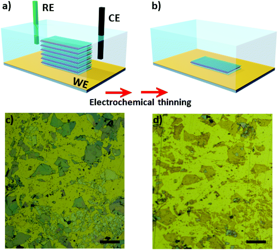 | ||
| Fig. 1 (a) Schematic view of the three-electrode cell. (b) Illustrative image of the electrode after electrochemical thinning process showing that bulk flakes are thinned down to monolayer. Optical microscope images of the electrodes containing MoS2 flakes before (c) and after (d) electrochemical experiments. Scale bars are 100 μm. | ||
Optical microscopy was used as first inspection of the samples. Fig. 2a and b shows MoS2 flake before and after the electrochemical step, respectively. The color change from light grey to brownish yellow indicates that the thinning process was well succeeded. In addition, more than 90% of bulk regions were removed by treating the images in Fig. 2a and b using image J software, as it will be shown ahead. The thickness of the flake before and after the thinning process was measured using AFM, as shown in Fig. 2c and d, respectively. The thickness of the flake illustrated in Fig. 2c was initially 143 nm, thus confirming the bulk nature of MoS2. The thickness of bulk flakes on gold substrates were found in the range of 100–500 nm. After the electrochemical process, height profiles indicated that MoS2 edges were thicker than basal plane (Fig. S1†). The thickness of inner regions of the flake was 0.8 nm, which is close to a monolayer.
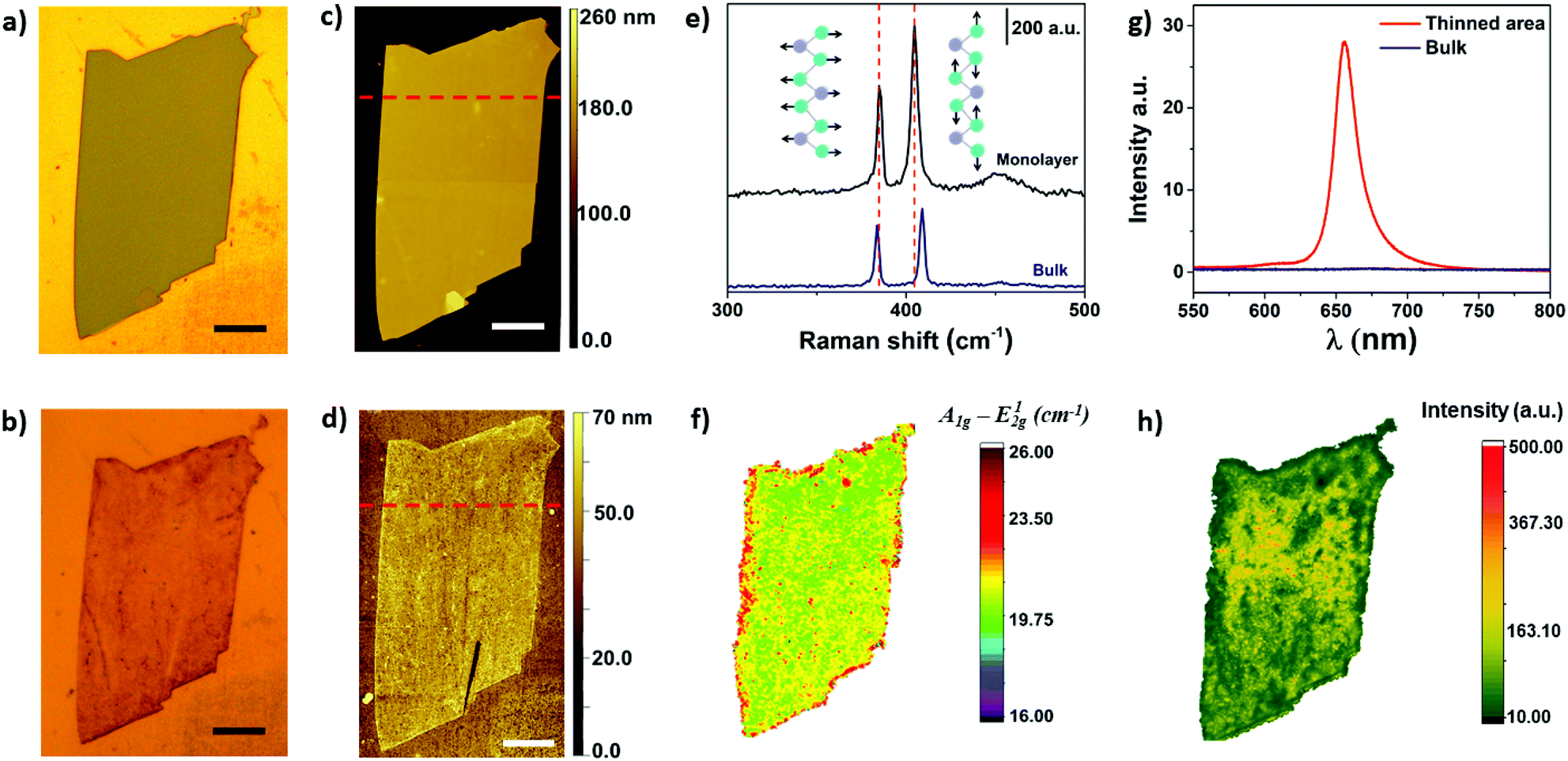 | ||
| Fig. 2 Optical (a, b) and AFM images (c, d) of MoS2 flakes before (a, c) and after (b, d) electrochemical thinning. Scale bars are 20 μm. (e) Raman spectra of bulk and monolayer regions. (f) Raman map of electrochemically thinned MoS2 flake. (g) Photoluminescence (PL) spectra of thinned and bulk areas. (h) PL map of the electrochemically thinned MoS2 crystal. PL intensity in (g) and (h) was normalized by A1g mode. | ||
Raman spectroscopy is commonly used to verify the number of MoS2 layers. The E12g (in plane vibration) and A1g (out-of-plane) Raman-active modes of 2H MoS2 can be detected in the range of 380 to 410 cm−1, approximately.35,36 In addition, the frequency difference between E12g and A1g can be used to monitor layer thickness (1 to 5 layers).37Fig. 2e shows representative Raman spectra of a MoS2 flake before and after electrochemical thinning. As can be observed, the frequency difference of the flake decreased from 25 cm−1 (bulk) to less than 20 cm−1 (monolayer). The Raman map illustrated in Fig. 2f shows a very homogeneous frequency difference on the basal plane, indicating that bulk layers were thinned down to monolayer. The red color observed on the edges suggest the presence of bulk residues, which are in agreement with the AFM results. We extended the wavenumber range in the Raman experiments to verify some additional information. Fig. S2† shows the Raman spectra in the range of 100 up to 1000 cm−1. We did not observe peaks in the range of 150 to 350 cm−1, indicating that no phase transition from 2H to 1T occurred after thinning.38
Photoluminescence experiments were also performed on bulk and electrochemically thinned MoS2 materials. The PL intensity of MoS2 is drastically increased when number of layers is reduced down to a monolayer.39,40 Such difference is associated with the electronic band structure of MoS2 that changes from indirect (bulk) to direct band-gap structure (monolayer). In addition, it has been reported that emission of photons with energy of ∼1.9 eV are associated with the presence of MoS2 monolayers.39Fig. 2g shows the PL spectra of MoS2 before and after the electrochemical thinning process. The spectrum shows peaks at 656 and 607 nm than can be associated with the presence of excitons A and B from the Brillion zone, respectively. Moreover, a long low-energy tail can also be observed in Fig. 2g for the electrochemically thinned MoS2 that can be attributed to the presence of trions.41 The later are negatively charged excitons (A−) centered at approximately 666 nm and observed in monolayer MoS2.42 Therefore, the high intensity of the A exciton after the electrochemical thinning process further indicates that the number of layers were thinned down to a monolayer. In addition, the peak position attributed to A exciton, located at 656 nm (∼1.89 eV), is in good agreement with the values reported in literature for monolayer MoS2.43 The PL map illustrated in Fig. 2h shows a more homogeneous PL intensity in the center region of the exfoliated flake. At the edges, the PL intensity was lower due to the presence of bulk residues, as described above.
The thinning process was investigated by cyclic voltammetry (CV) using microelectrodes to observe the contribution of a single flake. Fig. 3a depicts the CVs of a bare microfabricated Au electrode. In the anodic direction the current increases at approximately 1.3 V, which is consistent with the potential where the oxidation of gold take place.45 In the back scan, two peaks were observed at ∼0.9 V and 0.6 V. The peak at 0.9 V is attributed to the reduction of the gold oxide formed during the anodic scan while the peak at 0.6 V is due to reduction of the Cr that arises from the adhesion layer. It was demonstrated that the electrolyte can reach the adhesion layer due to the presence of pinholes on the gold film.46 In the presence of MoS2 a large oxidation peak can be observed in the cyclic voltammogram, as can be observed in Fig. 3b. The peak current at approximately 1.5 V decreases with the cycling process due to the thinning process. As can be observed in Fig. 3c–f, the thinning process advances as the number of cycles increases. The decrease in peak current was found to be dependent on the thickness of the bulk MoS2 flake in the range of 60 to 480 nm. A single 60 nm thick MoS2 flake was almost completely thinned on the first cycle, as illustrated in Fig. S3.† By comparing the peak current for microelectrodes containing 345 and 480 nm thick single flakes with very similar areas, as illustrated in Fig. 3b and S3,† it is possible to observe that more cycles are necessary for the thinning process using the thicker flake.
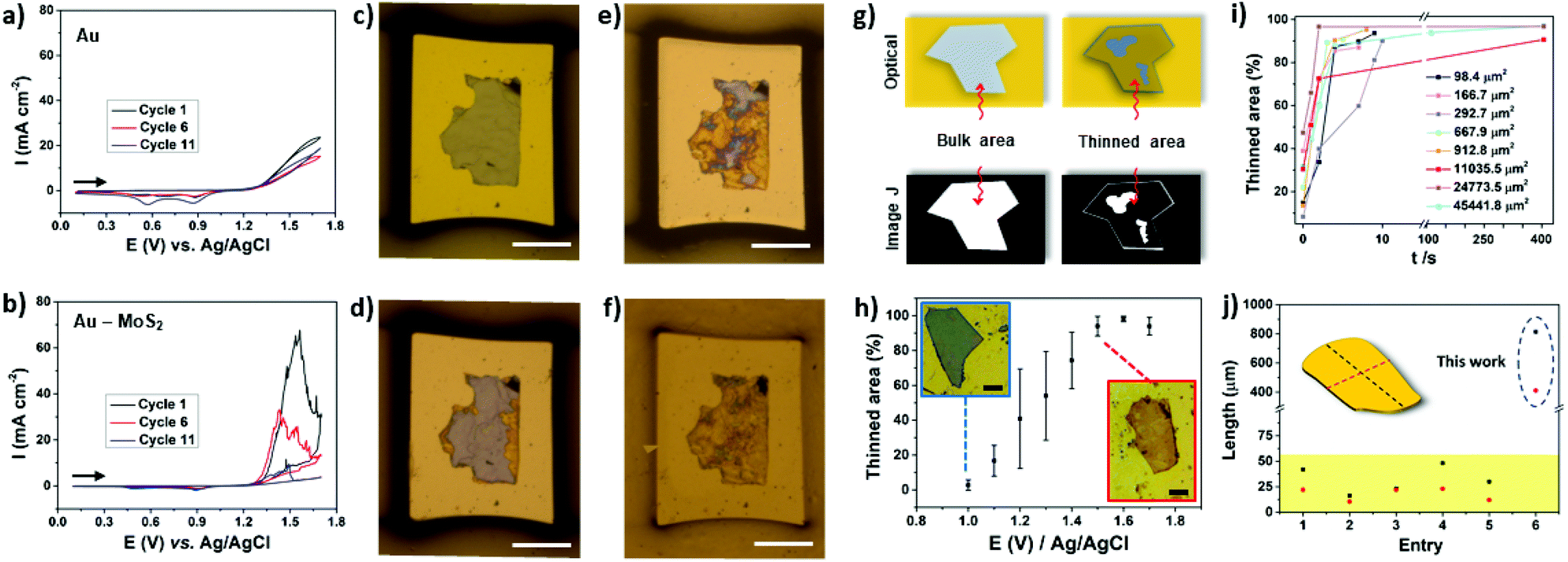 | ||
| Fig. 3 Cyclic voltammograms (CVs) obtained for (a) Au and (b) Au–MoS2 (tflake = 345 nm) electrodes in 0.5 M H2SO4 at 50 mV s−1. The current was normalized by the geometric area of the electrodes. Stereomicroscope images of the electrodes (Au–MoS2) before the experiment (c) and after cycle 1 (d), cycle 6 (e) and cycle 11 (f). The area and thickness of the MoS2 flake are 19714 μm2 and 345 nm, respectively. The scale bars in c–f are 100 μm. (g) Scheme illustrating the treatment by image J software. (h) Influence of the applied potential on thinned area. Scale bars are 25 μm. (i) Thinned area versus time. (j) Comparison of lateral flake sizes with different works in literature. Red and black dashed lines represent width and length, respectively. Entry: [1],31 [2, 3],30 [4]32 and [5].44 | ||
Next, we focused our study to obtain more information of the thinning process using image treatment. By obtaining optical images before and after the electrochemical process it is possible to investigate the influence of the applied potential and thinning time over the efficacy of the electrochemical treatment. The colors of bulk and electrochemically thinned MoS2 after image treatment were converted to white and black, respectively, as schematically illustrated in Fig. 3g. This process allowed us to estimate the thinned area at different experimental conditions. Fig. 3h shows the influence of the applied potential. At 1.0 V, the thinned process was observed only at the edges of the flakes, resulting in low thinned areas, less than 10%. As the applied potential was moved up to 1.7 V, the thinned area was remarkably increased. The curve reached a plateau in 1.5 V, resulting in thinned areas higher than 90%. Fig. 3i shows that the electrochemical process is fast, reaching 90% of thinned areas in less than 60 s for different flake sizes. As can be observed, larger flakes need more time to reach higher thinning yields. Fig. S4† shows an ultra-large MoS2 flake thinned by the proposed electrochemical route. Based on these results, oxidation time plays an important role to obtain large-area thinned MoS2 with minimum of bulk residues on the basal plane. Notably, the electrochemical process over large areas resulted in thinned areas with high yield. As it can be observed in Fig. 3j, remarkably, the lateral dimensions of the thinned MoS2 flake presented in this work surpasses the most recent works. We tested the thinning process on FTO using similar conditions but some regions of MoS2 were lixiviated (Fig. S5†).
Hyphenation of techniques allows us to obtain complementary, in situ, and real-time information about the electrochemical thinning process that occurs on the MoS2 flake deposited on Au electrodes. A compact electrochemical cell was mounted on the mechanical stage of an optical microscope using miniaturized reference and counter electrodes, as schematically shown in Fig. 4a. An representative chronoamperometric curve is presented in Fig. 4b. It is observed that the electrochemical thinning process is ultra-fast, as illustrated in the sequence of frames shown in Fig. 4c. The thinned flakes can be clearly visualized by color changes from light grey (bulk MoS2) to yellowish (monolayer MoS2). The arrows, in the image indicate that the thinning process start at the edges and rapidly moves into direction to the central regions of the flake. When the current decreased to their minimum values in the chronoamperograms more than 90% of the flake reached few to monolayer. Fig. 4d and e shows the pictures of the flake before and after the electrochemical process on Au electrodes, respectively. The Raman maps clearly illustrates that the thinning process mostly generates monolayer regions on the basal plane, illustrated by the green regions on the map shown in Fig. 4f.
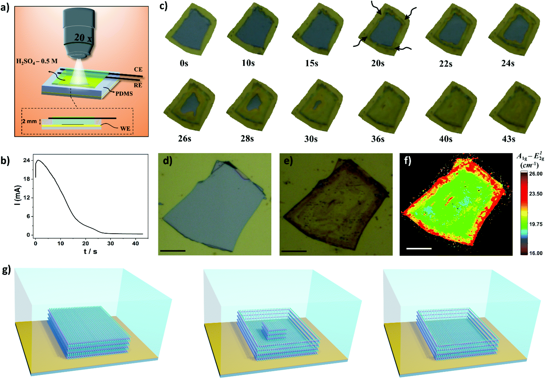 | ||
| Fig. 4 (a) Schematic view of the miniaturized electrochemical cell. (b) Chronoamperometric curve for the electrochemical thinning process. E = 1.5 V vs. Ag/AgCl (c) Sequence of images obtained during the electrochemical process. The height of the electrolyte is approximately 2 mm. (d and e) Pictures of MoS2 before and after the process. (f) Raman map of the MoS2 layer. Scale bars for figures d, e, f are 25 μm. (g) Schematic illustration of the evolution of MoS2 flakes during the electrochemical thinning process. | ||
By considering the microscopy-electrochemistry and previous characterization studies it is possible to draw the following scenario for the thinning process, as schematically shown in Fig. 4g. The bulk MoS2 crystals adsorbed onto Au electrodes are initially electrochemically thinned at the flake edges. The following reaction is proposed to occur on the material:44
| MoS2 + 8H2O → Mo6+ + 2SO42− + 16H+ + 18e− | (1) |
We also investigated the influence of dissolved oxygen over the thinning process. MoS2 flakes were thinned in the same extend in the presence and absence of O2 in electrolyte solution, as shown in Fig. S6.† One should note that in the potential region used to promote the thinning process with high yield, i.e. 1.5–1.7 V, O2 bubbling also occurs on gold electrodes using H2SO4 as electrolyte.47 As the thinning process advances into inner regions of the flake a remaining bulk region is left on the edges. The bulk region can be seen on images illustrated in Fig. 4c after 22 s (dark regions at the edges) and it was further confirmed by AFM and Raman experiments. As the electrochemical oxidation proceeds, the bulk island on the center region of the flake is slowly thinned resulting in a terrace that is predominately monolayer. In addition, we investigated the impact of the thickness of the bulk flakes before the thinning process on the width of the bulk regions left on the edges after the electrochemical step. The width of this region increases as a function of the thickness of the bulk flake, as illustrated in Fig. S7.† Thus, in order to minimize the bulk region on the edges thinner flakes should be used.
The surface chemistry of the electrochemically thinned MoS2 layers at different times was assessed by X-ray photoelectron spectroscopy (XPS), as shown in Fig. 5. The Mo 3d spectra of MoS2 before electrochemical thinning, illustrated in Fig. 5a, revealed peaks at around 229.5, 232.6 and 235.7 eV that can be attributed to Mo4+ 3d5/2, Mo4+ 3d3/2 and Mo6+ 3d3/2. The S 2p1/2 and S 2p3/2 were found at 163.5 and 162.3 eV in the S region of Fig. 5a, as reported.31,48 The resulting Mo and S peaks are characteristic of MoS2 at the 2H phase with minimal oxidation, less than 2% for Mo6+. Fig. 5b–d reveals the evolution of XPS spectra at different electrochemical thinning times, from 5 up to 240 s. We noticed that percentage of Mo6+ increased to 6% after 240 s of thinning time, indicating partial oxidation of MoS2 after electrochemical experiments. Despite this increase, the percentage of Mo6+ is considered low when compared with other works.49 At the S region, we observed a small peak at 164.5 eV,50 indicating the presence of bridging S22− and/or S2− in MoSx on the surface at 20 s and 240 s.
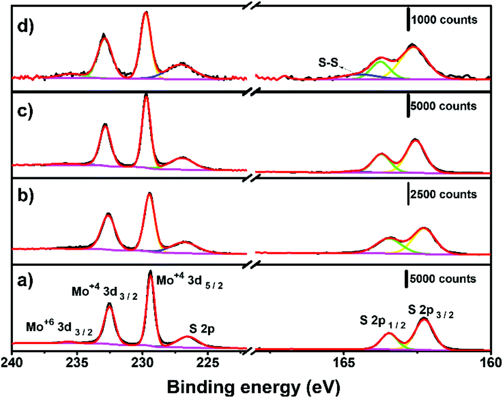 | ||
| Fig. 5 XPS spectra for (a) bulk MoS2 and at different electrochemical thinning times: (b) 5 s, (c) 20 s and (d) 240 s. | ||
Pan et al. connected Au tracks using electron beam litography process only at the edges of bulk MoS2 and performed a thinning process using voltammetry.44 In this lateral contact configuration, where MoS2 is seated on insulating surface, the thinning process start at the edges, but the thinning yield is low. The thickness of the edges is reduced but large thinned areas are not obtained in this type of electrode configuration. Here, bulk MoS2 flakes are seated on Au electrodes (bottom contact) achieving higher thinning yields. In addition to the effect of electrode contact, we can also consider the ultra-large aspect ratio reported in this work due to the high affinity of monolayer MoS2 with the Au substrate.14,51 In addition, the large-area MoS2 have more anchoring regions with substrate and allows the preparation of even more complex surfaces, as will be shown ahead.
Finally, as a proof-of-concept, we demonstrated the unprecedented preparation of free-standing and thin MoS2 layers by electrochemical thinning process. Free-standing MoS2 has been studied from theoretical aspects52,53 to experimental approaches. The later have been used to investigate mechanical,54 optical properties,55 and electrical features,56 along with application in biosensing assays.57 In addition, large free-standing layers holds the promise to work as optical windows to interface dry and wet environments, enabling new fundamental studies in health and energy fields.58 In brief, we fabricated flexible conductive microhole-structured Ni meshes electrochemically coated with Au thick films (1.5 μm), as recently reported.59Fig. 6a and b shows photos of these flexible Au meshes. Microholes separated by 35 μm from each other and with a diameter of approximately 18 μm can be observed in Fig. 6c. The area between the microholes guaranteed the interaction of MoS2 with the Au substrate. Fig. 6d and e illustrates optical images of MoS2 flakes before and after the thinning process, respectively. As confirmed by Raman measurements, the flakes were thinned down to a monolayer on the Au surface in this case.
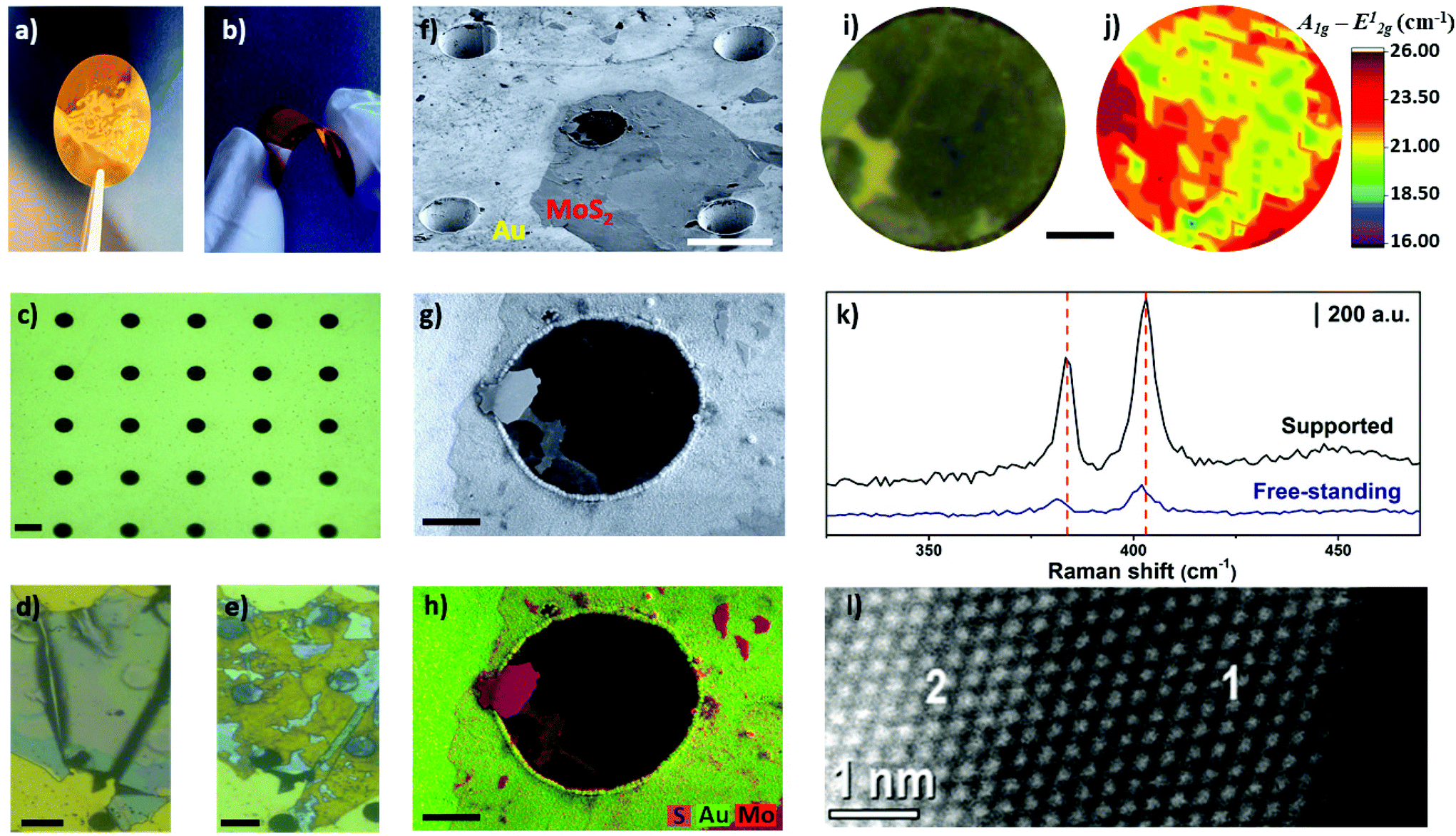 | ||
| Fig. 6 (a and b) Photos of the microhole-structured Ni/Au mesh. (c) Optical microscopy image of the Au mesh. Scale bar is 20 μm. (d and e) Optical microscopy images of the MoS2 flakes before and after electrochemical thinning process, respectively. Scale bar is 25 μm. (f) Tilted secondary electron SEM image of the thinned flake on the Au micromesh. Scale bar is 25 μm. (g and h) High-magnification secondary electron SEM image of thinned area on the microhole and EDS map, respectively. Scale bar is 5 μm. (i and j) Optical microscope image of the microhole region and Raman map, respectively. Scale bar is 5 μm. (k) Raman spectra obtained on supported and free-standing areas as indicated. (l) HAADF-HRSTEM image of the electrochemically thinned MoS2 layer. The inset numbers 1 and 2 indicated mono and bilayer regions, respectively. | ||
Interestingly, bulk MoS2 flakes were also thinned on the region over the microholes, resulting in the formation of mono-bilayer free-standing MoS2 layers. Remarkably, the free-standing diameter (18 μm) is at least four times higher when compared with most studies using MoS2 mono and few-layer,37,39,54,60 highlighting the feasibility of the method to create large-area free-standing layers. Tilted SEM analysis with an angle of 54 degrees illustrated in Fig. 6f shows that the microhole located in the center of the image was covered by an ultrathin material. Fig. 6g and h shows secondary electron SEM and EDS images, respectively. The bulk regions of MoS2 are clearly identified by the high intensity pink-red areas in image 6 h. The light pink-red areas show the thinned MoS2 regions, including on the center of the microhole.
The region of the MoS2 flake over the microhole was selected for additional investigation by Raman spectroscopy, as shown in Fig. 6i and j. The resulting Raman map indicated that the frequency difference ranged from 19–21.5 cm−1 in some areas, thus confirming that light pink-red areas observed in SEM-EDS images are mono-bilayer regions. In addition, Fig. 6k shows Raman spectra taken in free-standing and supported areas. A red-shift was observed for both A1g and E12g modes for the spectra obtained over the microhole. This result is in agreement with the Raman spectra reported for free-standing layers on microholes61 and wrinkled MoS2 prepared on elastomeric substrates.62 Height profiles obtained by AFM indicated that MoS2 layer advanced 200–250 nm into deeper regions of the microhole (Fig. S8†), which contributes to create strain in the 2D material. Such phenomenon is likely the cause of this red-shift as noted herein and in the literature for free-standing MoS2 layers. In addition, HAADF-HRSTEM image confirmed the presence of mono-bilayer regions, as illustrated in Fig. 6l.
Conclusions
In this work, we reported a simple and fast electrochemical thinning process to obtain ultra-large MoS2 monolayers on Au substrates. Bulk MoS2 flakes transferred to the conductive substrates are thinned down to a monolayer with more than 90% of initial bulk area being removed at potentials in the range of 1.5–1.7 V. The influence of the applied potential was assessed by image treatment, highlighting the possibility to roughly tune the thinning area by controlling oxidation potential. Bulk residues are mainly located at the flake edges while the basal plane presented large-area mono-bilayer regions, as confirmed by atomic force microscopy, photoluminescence and Raman experiments. Real-time visualization of the thinning process was achieved through the hyphenation of optical microscopy and electrochemistry, revealing that the thinning process starts at the edges and moves in the direction of the center of the flake. Moreover, hyphenation of techniques was used to investigate the thinning time, revealing the impact of the process on a wide range of flake sizes. We demonstrated the thinning process in ultra large-area MoS2 that can reach approximately 813.5 × 411 μm by adjusting the thinning time. Thus, our rote is very promising toward preparation of centimeter-scale monolayer MoS2 that could be used in the field of energy storage, such as lithium–sulfur batteries. Development of those novel energy-storage devices, with high gravimetric energy density beyond the traditional lithium-ion batteries, still demand ways to overcome performance losses due to the dissolution of lithium polysulfides species (Li2Sn, n = 4–8) into electrolytes. Yet, the best strategy is to use materials that are able to trap solution Li2Sn intermediates, and MoS2 monolayers withstand as one of these promising materials due its large surface area and good catalytic activity or the formation and the decomposition of Li2S in discharge and charge processes.63,64The preparation of free-standing mono-bilayer MoS2 using electrochemical thinning from bulk crystals was demonstrated for the first time on Au micromeshes. Despite its preliminary character, the electrochemical thinning process of MoS2 was found to successfully occur on regions that are not in contact with the conductive substrate, i.e., over microholes, resulting in large free-standing areas. Thus, the proposed work opens up the possibility to study mechanical, optical and electrochemical properties of ultra-large strained MoS2 layers. In addition, further efforts may extend its applicability to other 2D materials than can be thinned by electrochemical routes.
Author contributions
N. F. and B. R. F. contributed equally to this work and performed the transfer process, electrochemical thinning and characterization studies. J. B. and C. A. O. performed HRSTEM analysis. M. Strauss helped with Raman and PL measurements. V. M. S. F., M. H. O. P. and A. L. G. designed and prepared the meshes. M. Strauss, R. S. L. and E. R. L. helped with discussions. M. S. conceived the idea, designed the experiments and wrote the manuscript.Conflicts of interest
The authors Murilo Santhiago, Nicolli de Freitas and Bianca R. Florindo are listed as inventors on a patent filing application describing this technology.Acknowledgements
This work was supported by the Serrapilheira Institute (grant number: Serra-1912-31228). We thank Mariane P. Pereira, Davi H. Camargo, Fabiano E. Montoro, Otávio Berenguel, Carolina. P. Torres, Carlos A. R. Costa, and Cleyton A. Biffe for their help in this work with instrumentation and laboratory facilities. We also thank SisNano for the support.References
- W. Zheng, Y. Jiang, X. Hu, H. Li, Z. Zeng, X. Wang and A. Pan, Adv. Opt. Mater., 2018, 6, 1800420 CrossRef.
- Y. Liu, N. O. Weiss, X. Duan, H.-C. Cheng, Y. Huang and X. Duan, Nat. Rev. Mater., 2016, 1, 16042 CrossRef CAS.
- H. H. Huang, X. Fan, D. J. Singh and W. T. Zheng, Nanoscale, 2020, 12, 1247–1268 RSC.
- W. Li, X. Qian and J. Li, Nat. Rev. Mater., 2021, 6, 829–846 CrossRef CAS.
- C. Yim, V. Passi, M. C. Lemme, G. S. Duesberg, C. Ó. Coileáin, E. Pallecchi, D. Fadil and N. McEvoy, npj 2D Mater. Appl., 2018, 2, 5 CrossRef.
- T. Tan, X. Jiang, C. Wang, B. Yao and H. Zhang, Adv. Sci., 2020, 7, 2000058 CrossRef CAS.
- Y. Yuan, H. Lv, Q. Xu, H. Liu and Y. Wang, Nanoscale, 2019, 11, 4318–4327 RSC.
- A. Bolotsky, D. Butler, C. Dong, K. Gerace, N. R. Glavin, C. Muratore, J. A. Robinson and A. Ebrahimi, ACS Nano, 2019, 13, 9781–9810 CrossRef CAS PubMed.
- Y. He, P. Tang, Z. Hu, Q. He, C. Zhu, L. Wang, Q. Zeng, P. Golani, G. Gao, W. Fu, Z. Huang, C. Gao, J. Xia, X. Wang, X. Wang, C. Zhu, Q. M. Ramasse, A. Zhang, B. An, Y. Zhang, S. Martí-Sánchez, J. R. Morante, L. Wang, B. K. Tay, B. I. Yakobson, A. Trampert, H. Zhang, M. Wu, Q. J. Wang, J. Arbiol and Z. Liu, Nat. Commun., 2020, 11, 57 CrossRef CAS PubMed.
- C. Wu, J. Zhang, X. Tong, P. Yu, J. Xu, J. Wu, Z. M. Wang, J. Lou and Y. Chueh, Small, 2019, 15, 1900578 CrossRef PubMed.
- M. S. Sokolikova and C. Mattevi, Chem. Soc. Rev., 2020, 49, 3952–3980 RSC.
- A. T. Hoang, K. Qu, X. Chen and J.-H. Ahn, Nanoscale, 2021, 13, 615–633 RSC.
- F. Liu, W. Wu, Y. Bai, S. H. Chae, Q. Li, J. Wang, J. Hone and X.-Y. Zhu, Science, 2020, 367, 903–906 CrossRef CAS PubMed.
- M. Velický, G. E. Donnelly, W. R. Hendren, S. McFarland, D. Scullion, W. J. I. DeBenedetti, G. C. Correa, Y. Han, A. J. Wain, M. A. Hines, D. A. Muller, K. S. Novoselov, H. D. Abruña, R. M. Bowman, E. J. G. Santos and F. Huang, ACS Nano, 2018, 12, 10463–10472 CrossRef PubMed.
- Y. Huang, Y.-H. Pan, R. Yang, L.-H. Bao, L. Meng, H.-L. Luo, Y.-Q. Cai, G.-D. Liu, W.-J. Zhao, Z. Zhou, L.-M. Wu, Z.-L. Zhu, M. Huang, L.-W. Liu, L. Liu, P. Cheng, K.-H. Wu, S.-B. Tian, C.-Z. Gu, Y.-G. Shi, Y.-F. Guo, Z. G. Cheng, J.-P. Hu, L. Zhao, G.-H. Yang, E. Sutter, P. Sutter, Y.-L. Wang, W. Ji, X.-J. Zhou and H.-J. Gao, Nat. Commun., 2020, 11, 2453 CrossRef CAS PubMed.
- Q. Zhang, L. Mei, X. Cao, Y. Tang and Z. Zeng, J. Mater. Chem. A, 2020, 8, 15417–15444 RSC.
- G. Eda, H. Yamaguchi, D. Voiry, T. Fujita, M. Chen and M. Chhowalla, Nano Lett., 2011, 11, 5111–5116 CrossRef CAS PubMed.
- Á. Coogan and Y. K. Gun'ko, Mater. Adv., 2021, 2, 146–164 RSC.
- P. Yang, X. Zou, Z. Zhang, M. Hong, J. Shi, S. Chen, J. Shu, L. Zhao, S. Jiang, X. Zhou, Y. Huan, C. Xie, P. Gao, Q. Chen, Q. Zhang, Z. Liu and Y. Zhang, Nat. Commun., 2018, 9, 979 CrossRef PubMed.
- Y. Huang, J. Wu, X. Xu, Y. Ho, G. Ni, Q. Zou, G. K. W. Koon, W. Zhao, A. H. Castro Neto, G. Eda, C. Shen and B. Özyilmaz, Nano Res., 2013, 6, 200–207 CrossRef CAS.
- M. Yamamoto, T. L. Einstein, M. S. Fuhrer and W. G. Cullen, J. Phys. Chem. C, 2013, 117, 25643–25649 CrossRef CAS.
- Y. Liu, H. Nan, X. Wu, W. Pan, W. Wang, J. Bai, W. Zhao, L. Sun, X. Wang and Z. Ni, ACS Nano, 2013, 7, 4202–4209 CrossRef CAS PubMed.
- K. K. Amara, L. Chu, R. Kumar, M. Toh and G. Eda, APL Mater., 2014, 2, 092509 CrossRef.
- Y. Yang, H. Hou, G. Zou, W. Shi, H. Shuai, J. Li and X. Ji, Nanoscale, 2019, 11, 16–33 RSC.
- L. Li, D. Zhang, Y. Gao, J. Deng, Y. Gou and J. Fang, J. Alloys Compd., 2021, 862, 158551 CrossRef CAS.
- K. Sunamura, T. R. Page, K. Yoshida, T. Yano and Y. Hayamizu, J. Mater. Chem. C, 2016, 4, 3268–3273 RSC.
- A. Ambrosi and M. Pumera, Chem. Soc. Rev., 2018, 47, 7213–7224 RSC.
- S. García-Dalí, J. I. Paredes, J. M. Munuera, S. Villar-Rodil, A. Adawy, A. Martínez-Alonso and J. M. D. Tascón, ACS Appl. Mater. Interfaces, 2019, 11, 36991–37003 CrossRef PubMed.
- A. Ambrosi and M. Pumera, Chem. – Eur. J., 2018, 24, 18551–18555 CrossRef CAS PubMed.
- A. Sebastian, F. Zhang, A. Dodda, D. May-Rawding, H. Liu, T. Zhang, M. Terrones and S. Das, ACS Nano, 2019, 13, 78–86 CrossRef CAS.
- N. Liu, P. Kim, J. H. Kim, J. H. Ye, S. Kim and C. J. Lee, ACS Nano, 2014, 8, 6902–6910 CrossRef CAS PubMed.
- S. Das, M. K. Bera, S. Tong, B. Narayanan, G. Kamath, A. Mane, A. P. Paulikas, M. R. Antonio, S. K. R. S. Sankaranarayanan and A. K. Roelofs, Sci. Rep., 2016, 6, 28195 CrossRef CAS PubMed.
- D. S. Schulman, D. May-Rawding, F. Zhang, D. Buzzell, N. Alem and S. Das, ACS Appl. Mater. Interfaces, 2018, 10, 4285–4294 CrossRef CAS PubMed.
- T. Hong, T. Shen, J. Yang, Y. Sun, J. Zhang, H. Pan, Y. Hong, Y. Wang, S. Chen, Y. Zhao and C. F. Guo, Int. J. Smart. Nano Mater., 2020, 11, 1–10 CrossRef.
- K.-G. Zhou, F. Withers, Y. Cao, S. Hu, G. Yu and C. Casiraghi, ACS Nano, 2014, 8, 9914–9924 CrossRef CAS PubMed.
- H. Li, Q. Zhang, C. C. R. Yap, B. K. Tay, T. H. T. Edwin, A. Olivier and D. Baillargeat, Adv. Funct. Mater., 2012, 22, 1385–1390 CrossRef CAS.
- C. Lee, H. Yan, L. E. Brus, T. F. Heinz, J. Hone and S. Ryu, ACS Nano, 2010, 4, 2695–2700 CrossRef CAS PubMed.
- J. Huang, X. Pan, X. Liao, M. Yan, B. Dunn, W. Luo and L. Mai, Nanoscale, 2020, 12, 9246–9254 RSC.
- K. F. Mak, C. Lee, J. Hone, J. Shan and T. F. Heinz, Phys. Rev. Lett., 2010, 105, 136805 CrossRef PubMed.
- M. Seol, M. Lee, H. Kim, K. W. Shin, Y. Cho, I. Jeon, M. Jeong, H. Lee, J. Park and H. Shin, Adv. Mater., 2020, 32, 2003542 CrossRef CAS.
- J. W. Christopher, B. B. Goldberg and A. K. Swan, Sci. Rep., 2017, 7, 14062 CrossRef PubMed.
- T. F. D. Fernandes, A. de C. Gadelha, A. P. M. Barboza, R. M. Paniago, L. C. Campos, P. S. Soares Guimarães, P.-L. de Assis and B. R. A. Neves, 2D Mater., 2018, 5, 025018 CrossRef.
- M. Buscema, G. A. Steele, H. S. J. van der Zant and A. Castellanos-Gomez, Nano Res., 2014, 7, 561–571 CrossRef.
- X. Pan, M. Yan, C. Sun, K. Zhao, W. Luo, X. Hong, Y. Zhao, L. Xu and L. Mai, Adv. Funct. Mater., 2021, 31, 2007840 CrossRef CAS.
- X. Xu, A. Makaraviciute, J. Pettersson, S.-L. Zhang, L. Nyholm and Z. Zhang, Sens. Actuators, B, 2019, 283, 146–153 CrossRef CAS.
- J. C. Hoogvliet and W. P. van Bennekom, Electrochim. Acta, 2001, 47, 599–611 CrossRef CAS.
- J. D. Benck, B. A. Pinaud, Y. Gorlin and T. F. Jaramillo, PLoS One, 2014, 9, e107942 CrossRef PubMed.
- F. Wu, Z. Liu, N. Hawthorne, M. Chandross, Q. Moore, N. Argibay, J. F. Curry and J. D. Batteas, ACS Nano, 2020, 14, 16939–16950 CrossRef CAS PubMed.
- F. Li, F. Gao, M. Xu, X. Liu, X. Zhang, H. Wu and J. Qi, Adv. Mater. Interfaces, 2018, 5, 1800348 CrossRef.
- R. Ding, Y. Liu, M. Wang, L. Qin, X. Cui, C. Wang, L. Wang and B. Lv, Electrochim. Acta, 2017, 248, 20–28 CrossRef CAS.
- M. Velický, A. Rodriguez, M. Bouša, A. V. Krayev, M. Vondráček, J. Honolka, M. Ahmadi, G. E. Donnelly, F. Huang, H. D. Abruña, K. S. Novoselov and O. Frank, J. Phys. Chem. Lett., 2020, 11, 6112–6118 CrossRef PubMed.
- S. Ghaderzadeh, V. Ladygin, M. Ghorbani-Asl, G. Hlawacek, M. Schleberger and A. V. Krasheninnikov, ACS Appl. Mater. Interfaces, 2020, 12, 37454–37463 CrossRef CAS PubMed.
- J. Jiang, L. Wang and Y. Zhang, J. Appl. Phys., 2019, 126, 135106 CrossRef.
- S. Manzeli, D. Ovchinnikov, D. Pasquier, O. V. Yazyev and A. Kis, Nat. Rev. Mater., 2017, 2, 17033 CrossRef CAS.
- K. Kojima, H. E. Lim, Z. Liu, W. Zhang, T. Saito, Y. Nakanishi, T. Endo, Y. Kobayashi, K. Watanabe, T. Taniguchi, K. Matsuda, Y. Maniwa, Y. Miyauchi and Y. Miyata, Nanoscale, 2019, 11, 12798–12803 RSC.
- W. M. Parkin, A. Balan, L. Liang, P. M. Das, M. Lamparski, C. H. Naylor, J. A. Rodríguez-Manzo, A. T. C. Johnson, V. Meunier and M. Drndić, ACS Nano, 2016, 10, 4134–4142 CrossRef CAS PubMed.
- N. Masurkar, N. K. Thangavel, S. Yurgelevic, S. Varma, G. W. Auner and L. M. Reddy Arava, Biosens. Bioelectron., 2021, 172, 112724 CrossRef CAS PubMed.
- L. M. Meireles, I. D. Barcelos, G. A. Ferrari, P. A. A. de A. Neves, R. O. Freitas and R. G. Lacerda, Lab Chip, 2019, 19, 3678–3684 RSC.
- G. F. Giordano, V. M. S. Freitas, G. R. Schleder, M. Santhiago, A. L. Gobbi and R. S. Lima, ACS Appl. Mater. Interfaces, 2021, 13, 35914–35923 CrossRef CAS PubMed.
- X. Zhang, R. Zhang, X. Zheng, Y. Zhang, X. Zhang, C. Deng, S. Qin and H. Yang, Nanomaterials, 2019, 9, 796 CrossRef CAS PubMed.
- D. Lloyd, X. Liu, J. W. Christopher, L. Cantley, A. Wadehra, B. L. Kim, B. B. Goldberg, A. K. Swan and J. S. Bunch, Nano Lett., 2016, 16, 5836–5841 CrossRef CAS PubMed.
- A. Castellanos-Gomez, R. Roldán, E. Cappelluti, M. Buscema, F. Guinea, H. S. J. van der Zant and G. A. Steele, Nano Lett., 2013, 13, 5361–5366 CrossRef CAS PubMed.
- W. Cui, H. Li, Y. Liu, Q. Cai and J. Zhao, Physica E, 2021, 130, 114715 CrossRef CAS.
- S. Dong, X. Sun and Z. Wang, Beilstein J. Nanotechnol., 2019, 10, 774–780 CrossRef PubMed.
Footnote |
| † Electronic supplementary information (ESI) available: AFM images, electrochemical experiments and additional photos. See DOI: https://doi.org/10.1039/d2nr00491g |
| This journal is © The Royal Society of Chemistry 2022 |