
 Open Access Article
 This Open Access Article is licensed under a
 Creative Commons Attribution 3.0 Unported Licence
Engineering thermoelectric and mechanical properties by nanoporosity in calcium cobaltate films from reactions of Ca(OH)2/Co3O4 multilayers†
Binbin
Xin
 *a,
Erik
Ekström
a,
Yueh-Ting
Shih
b,
Liping
Huang
b,
Jun
Lu
a,
Anna
Elsukova
a,
Yun
Zhang
c,
Wenkai
Zhu
c,
Theodorian
Borca-Tasciuc
c,
Ganpati
Ramanath
ab,
Arnaud
Le Febvrier
a,
Biplab
Paul
a and
Per
Eklund
*a
*a,
Erik
Ekström
a,
Yueh-Ting
Shih
b,
Liping
Huang
b,
Jun
Lu
a,
Anna
Elsukova
a,
Yun
Zhang
c,
Wenkai
Zhu
c,
Theodorian
Borca-Tasciuc
c,
Ganpati
Ramanath
ab,
Arnaud
Le Febvrier
a,
Biplab
Paul
a and
Per
Eklund
*a
aThin Film Physics Division, Department of Physics, Chemistry and Biology (IFM), Linköping University, SE-58183 Linköping, Sweden. E-mail: binbin.xin@liu.se; per.eklund@liu.se
bDepartment of Materials Science and Engineering, Rensselaer Polytechnic Institute, Troy, New York 12180, USA
cRensselaer Polytechnic Institute, Department of Mechanical, Aerospace, and Nuclear Engineering, Troy, NY 12180, USA
First published on 4th July 2022
Abstract
Controlling nanoporosity to favorably alter multiple properties in layered crystalline inorganic thin films is a challenge. Here, we demonstrate that the thermoelectric and mechanical properties of Ca3Co4O9 films can be engineered through nanoporosity control by annealing multiple Ca(OH)2/Co3O4 reactant bilayers with characteristic bilayer thicknesses (bt). Our results show that doubling bt, e.g., from 12 to 26 nm, more than triples the average pore size from ∼120 nm to ∼400 nm and increases the pore fraction from 3% to 17.1%. The higher porosity film exhibits not only a 50% higher electrical conductivity of σ ∼ 90 S cm−1 and a high Seebeck coefficient of α ∼ 135 μV K−1, but also a thermal conductivity as low as κ ∼ 0.87 W m−1 K−1. The nanoporous Ca3Co4O9 films exhibit greater mechanical compliance and resilience to bending than the bulk. These results indicate that annealing reactant multilayers with controlled thicknesses is an attractive way to engineer nanoporosity and realize mechanically flexible oxide-based thermoelectric materials.
1. Introduction
The rapid development of autonomous, portable and wearable devices and sensors has sparked a great deal of interest in self-sustaining energy sources to replace batteries that are typically limited by shape constraints, periodic recharging and replacement.1,2 Harvesting electricity from heat using devices made from mechanically flexible thermoelectric materials is promising for such applications.3–6 Besides a high thermoelectric figure of merit ZT = α2σT/κ (α is the Seebeck coefficient, σ and κ the electrical and thermal conductivities, respectively, and T the absolute temperature7–9) for efficient energy conversion, properties such as high mechanical flexibility and toughness are key requirements.Conducting polymer-based organic thermoelectric materials are mechanically flexible and exhibit ZT values as high as 0.42,10–17 but are unsuitable for higher than near-room-temperature applications. Purely inorganic thermoelectrics18 are usually brittle. Integrating nanograined films or nanocrystal assemblies of inorganic thermoelectrics, e.g., Bi2−xSbxTe3, on flexible substrates that can withstand moderately high temperatures addresses these challenges to some extent, and yield α2σ values up to 0.2 mW m−1 K−2 at ∼200 °C.19,20 Semiconductors with extraordinary metal-like ductility, e.g., Ag2S, and Ag2Se also hold promise as free-standing thermoelectric materials that obviate flexible substrates.21–23
Oxide-based thermoelectric films on layered substrates such as mica offer greater stability at even higher temperatures and can become viable alternatives if high α and σ, are achieved together with high mechanical flexibility.24,25 Calcium cobaltate Ca3Co4O9 is an attractive p-type thermoelectric that exhibits inherently high α and high σ due to its layered crystal structure.26–30 The thermoelectric properties of layered cobaltates can be improved by nanostructuring, such as fabricating a high-quality single-phase,31,32 nanostructuring approaches,33 elemental doping,34 growing textured films with c-axis orientation.35 However, the thermal conductivity was normally increased with the improving electrical conductivity.36,37 Introducing nanoscale with dimensions mainly in the ranges of phonon mean free paths is a possible approach to reduce thermal conductivity without inhibiting electrical conductivity due to phonon mean free paths are typically significantly higher than electronic mean free paths. The textured nanograins and faceted nanopores not only offer additional means to lower the κ,38,39 but also alleviate the brittleness.40,41 Flexible porous nanograined Ca3Co4O9 films obtained by annealing CaO/CoO reactant multilayers exhibit power factors as high a 0.23 mW m−1 K−2 at room temperature.40 To further increase the porosity of nanoporous Ca3Co4O9 films retaining α and σ, it might be an effective way to further reduce κ and improve flexibility.
Here, we demonstrate that nanoporosity characteristics in Ca3Co4O9 films can be controlled by adjusting the reactant bilayer thickness in multilayer stacks. The porosities change from 11.2 to 17.1%. The nanoporous films show high σ with a narrow range from 80 to 95 S cm−1 and high α of ∼130 to ∼135 μV K−1, which are close to the values.42–44 The film with the highest porosity 17.1% has the lowest κ (∼0.87 W m−1 K−1). The nanoporous Ca3Co4O9 films exhibit greater mechanical compliance and resilience to bending than the bulk. Our findings showing pore engineering of layered-ceramics is attractive for realizing mechanically flexible thermoelectrics.
2. Experimental section
Nanoporous Ca3Co4O9 thin films were synthesized by annealing Ca(OH)2/Co3O4 multilayers on muscovite mica(00l) substrates. CaO/Co3O4 multilayers were deposited at 600 °C by reactive RF-magnetron sputtering from Ca and Co targets with a 2 mTorr plasma of a 0.5% O2/99.5% Ar gas mixture40. Ambient air-exposure of the CaO/Co3O4 multilayers for one month resulted in Ca(OH)2/Co3O4 multilayers via CaO hydration into Ca(OH)2.45 Subsequent annealing Ca(OH)2/Co3O4 multilayers at 700 °C for 2 hours in air led to nanoporous Ca3Co4O9 formation. We prepared five sets of multilayers with different Ca(OH)2/Co3O4 bilayer thicknesses, bt. The deposition times for CaO and Co3O4 were varied while keeping the total nominal multilayer thickness constant at ∼140 nm. The individual thicknesses of Ca(OH)2 and Co3O4 layers in each multilayer film were identical, i.e., bt/2. Thus, altering the bilayer thickness in the 12 ≤ bt ≤ 50 nm range is equivalent to varying the number of bilayers bn in the 21 ≥ bn ≥ 5 range.Phase identification was carried out by X-ray diffractometry (XRD) using a PANalytical X'Pert PRO instrument with monochromatic Cu Kα radiation (λ = 1.5406 Å) and a Ni filter. X-ray reflectivity (XRR) measurements were carried out in a PANalytical Empyrean diffractometer equipped with a copper Cu Kα source with a hybrid mirror on the incidence beam path, a triple-axis Ge 220 analyzer on the diffracted beam path, and a PIXcel3D detector operated in open detection mode. The XRR data were fitted using the X'Pert reflectivity program.
Scanning electron microscopy (SEM) and energy dispersive X-ray (EDX) spectroscopy were carried out in a LEO Gemini 1550 Zeiss instrument operated at 10 kV to characterize film morphology and composition. The surface porosity fraction was determined by analyses of SEM micrographs using the Java version of image J software46,47. Most of the nanopores were hexagonal in shape. The average nanopore sizes were estimated from the nanopore area with an uncertainty of 20%, by assuming all the pores to be regular hexagons. The average nanopore size is equal to L + 2L![[thin space (1/6-em)]](https://www.rsc.org/images/entities/char_2009.gif) cos60° where L is hexagon side length. Transmission electron microscopy (TEM) was carried out in a FEI Tecnai G2 TF20 UT instrument operated at 200 kV on multilayer cross-sections prepared by face-to-face gluing of two sample pieces and mounting them on a Ti grid. The samples were mechanically polished down to 50 μm and ion-milled in a Gatan system with 2–5 kV Ar+ beams incident at 5°.
cos60° where L is hexagon side length. Transmission electron microscopy (TEM) was carried out in a FEI Tecnai G2 TF20 UT instrument operated at 200 kV on multilayer cross-sections prepared by face-to-face gluing of two sample pieces and mounting them on a Ti grid. The samples were mechanically polished down to 50 μm and ion-milled in a Gatan system with 2–5 kV Ar+ beams incident at 5°.
Electrical conductivity σ was determined from the sheet resistance measured with a four-point probe Jandel RM3000 station and the film thickness determined from cross-sectional TEM images. Seebeck coefficient α was determined from the slope of the temperature gradient–voltage characteristics measured in a homemade Seebeck measurement setup system equipped with two K-type thermocouples placed at the same position as two Cu electrodes, a Keithley 2001 multimeter, two Peltier elements acting as temperature controller, and two thermometers45,48.
Thermal conductivity of the annealed Ca3Co4O9 film-on-mica samples was determined by non-contact scanning thermal microscopy (SThM) described elsewhere49–52. This technique utilizes a Joule-heated 5 μm-diameter Wollaston wire probe, whose thermal resistance was measured in air at 100 nm above the sample surface based on temperature-induced changes in the electrical resistance of the probe and the dissipated Joule heating power. For each film, we measured thermal resistance at three different locations on the sample surface. Thermal conductivity was determined by fitting the thermal resistance data with a 3D finite element model (3DFEM) of the probe-to-sample surface heat transfer assuming isotropic thermal properties for the films and the substrate.
Mechanical flexibility was evaluated by estimating the elastic moduli of the films by surface Brillouin scattering (SBS) spectroscopy and measuring bending-induced relative changes in electrical resistance. SBS spectra were collected by using a JSR Scientific Instruments six-pass high-contrast Fabry–Perot interferometer equipped with a 532.18 nm Verdi V2 DPSS green laser probe. Surface Rayleigh and Sezawa wave velocities were obtained by using V = (λ0Δf)/(2sinθs), where λ0 is the laser wavelength, Δf the Brillouin frequency shift, and θs the scattering angle.53 For the bending tests, we measured the normalized electrical resistance change ΔR/R0 for different bending radii and cycles, where the initial resistance R0 includes contact resistances. A constant resistance during bending corresponds to ΔR/R0 = 0 and indicates good mechanical flexibility and retention of electrical properties.
3. Results and discussion
X-ray diffractograms acquired immediately after deposition for all bt values investigated show 111 and 222 Bragg reflections from CaO besides those from the mica substrate (Fig. 1a). The 400 diffraction peaks reflected from Co3O4 is overwhelmed by a stronger 00l reflection from the mica substrate (Fig. 1a) but is observable in diffractograms from as-deposited films on sapphire (Fig. 1b). Films on sapphire also show a weak 111 peak from CoO. The CaO and Co3O4 peaks intensities, normalized to that of the 004 mica substrate reflection and sapphire reflection, increase with increasing bt (Fig. 1c). | ||
| Fig. 1 X-ray diffractograms from as-deposited CaO/Co3O4 multilayers with different bilayer thicknesses bt, on (a) mica (00l), and (b) sapphire (006) substrates. (c) CaO and Co3O4 peak intensities normalized with the intensity of the corresponding substrate peak, plotted as a function of bt. | ||
Air-exposure of the as-deposited multilayers growing on mica and sapphire leads to the diminution and eventual disappearance of the CaO 111 and 222 peaks (see Fig. 2a and b). Multilayers on sapphire also show a similar behaviour besides revealing a concomitant emergence of the Ca(OH)2 001 peak. This peak is not observable in diffractograms from films on mica due to substrate peak overlap. These results are indicative of the conversion of CaO to Ca(OH)2 through ambient moisture uptake.45 We note that the intensities of the Ca(OH)2 and Co3O4 peaks increase with increasing bt, the intensity of Ca(OH)2 is not the highest when the bt is 50 nm (Fig. 2c).
 | ||
| Fig. 2 X-ray diffractograms from Ca(OH)2/Co3O4 multilayers formed by air-exposure of CaO/Co3O4 multilayers with different bilayer thicknesses between 12 ≤ bt ≤ 50 nm on (a) mica (00l) and (b) sapphire (006) substrates. (c) Ca(OH)2 and Co3O4 peak intensities normalized to that of the 006 peak from the sapphire substrate, plotted as a function of bt. | ||
Air-exposed CaO/Co3O4 multilayers specified by low bt (e.g., ∼12 nm) consist of equiaxed grains of Ca(OH)2 and Co3O4 without any discernible interfaces (Fig. 3a). EDX spectral maps of Ca and Co indicate that Ca(OH)2 and Co3O4 are interspersed across individual layers (Fig. 3a inset). This result is consistent with Co3O4 layers comprised of discontinuous grains that facilitate moisture intake and transport, as suggested in our recent work.45 Air-exposed multilayers with bt = 16 nm exhibit more distinct Ca(OH)2/Co3O4 interfaces (Fig. 3b). The Ca-containing layers that appear brighter due to a higher Z-contrast are about 81% thicker than the Co3O4 layers, consistent with a 95.2% unit cell volume expansion caused by the CaO → Ca(OH)2 conversion during air-exposure. For bt > 16 nm, TEM images show distinct Co- and Ca-containing layers, but with a greater interface roughness that increases with bt. Such interface roughening is attributable to the higher volume Ca(OH)2 grains encroaching into the nearly unchanged adjacent Co3O4 layers. For bt = 50 nm, the thickness of Ca(OH)2 layer in top larger than that in bottle near mica, which may be due to the low hydration reactions by preventing of thicker Co3O4 layers and lead to the low intensity of Ca(OH)2 001 in Fig. 2c. SAED patterns indicate increased in-plane grain texturing with increasing bt (see Fig. 3c and d). EDX spectral maps from air-exposed films with higher bt show distinct Co-containing layers, in contrast to the uniform distribution of Ca, indicating Ca diffusion (see ESI Fig. S1†). Our results indicate that the bilayer thickness needs to be greater than a critical value of bt > 12 nm to form layers structure with sharp interfaces.
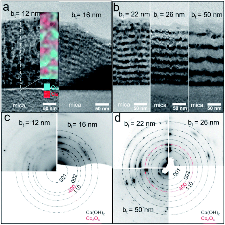 | ||
| Fig. 3 (a and b) Cross-sectional bright-field TEM images and (c and d) selected-area electron diffraction (SAED) patterns from Ca(OH)2/Co3O4 multilayers with different bilayer thicknesses bt. | ||
Otherwise, EDS maps from multilayers with bt = 16 nm show clear Co layers and almost uniform distribution Ca elements in multilayers (see ESI Fig. S1a†).
X-ray diffractograms show that annealing the Ca(OH)2/Co3O4 multilayers leads to Ca3Co4O9 formation through a reaction between the Co3O4 and Ca(OH)2 layers (Fig. 4a). The exclusive presence of multiple 00l peak reflections of Ca3Co4O9 indicate textured basal planes oriented parallel to the substrate surface. The Ca3Co4O9 grain size is largest for films specified by bt = 22 nm, as indicated by the narrowest width of the Ca3Co4O9 002 reflection.
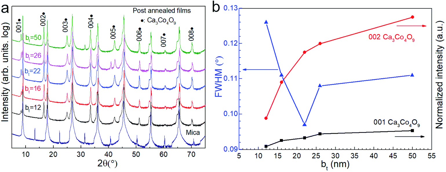 | ||
| Fig. 4 (a) X-ray diffractograms showing Ca3Co4O9 formation on mica (00l) substrate by annealing Ca(OH)2/Co3O4 multilayers with different bilayer thicknesses in the 12 ≤ bt ≤ 50 nm range. (b) Ca3Co4O9 001 and 002 peak intensities normalized with the intensity of the corresponding substrate peaks, plotted as a function of bt. | ||
Surfaces of the annealed films exhibit faceted intergranular nanopores (see Fig. 5). Films with the smallest bt in our studies reveal a relatively rough surface, probably due to the edge-on orientation of some platelet-shaped grains on the surface (see Fig. 5a). In contrast, annealed films with bt ≥ 16 nm exhibit smoother surfaces, with faceted nanopores between hexagonal terraces and plate-shaped grains (Fig. 5b–e). The average pore size increases monotonically from around 120 to 400 nm with increasing bt from 12 nm to 50 nm (see Fig. 5f). The porosity fraction increases with bt from 3.7% to 17.1% for 12 ≤ bt ≤ 26 nm but drops to 13.4% for bt = 50 nm (Fig. 5f).
 | ||
| Fig. 5 (a–e) SEM images from annealed Ca(OH)2/Co3O4 multilayers with 12 ≤ bt ≤ 50 nm grown on mica (00l) substrates. (f) Surface porosity fraction determined from SEM image analyses. | ||
Cross-sectional TEM micrographs of films obtained by annealing Ca(OH)2/Co3O4 multilayers with 12 ≤ bt ≤ 50 nm created from CaO/Co3O4 multilayers (Fig. 6a–e) reveal a polycrystalline Ca3Co4O9 layer separated from the substrate by an amorphous glass layer.40 Lattice images for the Ca3Co4O9 layer and SAED patterns (Fig. 6f–j) confirm that the (001) basal planes are oriented parallel to the film surface, corroborating our XRD and SEM results. The in-plane/out-of-plane aspect ratio of the pores is about four for the film with bt = 50 nm (Fig. 6e). This observation is consistent with the SEM results and our recent work45 indicating that oriented nanopore formation arises from basal plane removal driven by local densification of textured Ca3Co4O9. For all bt values except bt = 50 nm, we observe nanopores spanning across the Ca3Co4O9 layers and microporous gaps at the Ca3Co4O9 – amorphous layer interface and interlayer nanoporosity (see Fig. 6a–e). No microporous gaps or interlayer porosity are discernible in the amorphous layers.
 | ||
| Fig. 6 (a–e) Cross-sectional bright-field TEM images from Ca3Co4O9 films obtained by annealing Ca(OH)2/Co3O4 multilayers with 12 ≤ bt ≤ 50 nm created from CaO/Co3O4 multilayers. (f–j) The corresponding high-resolution TEM images and SAED patterns capturing the layered atomic structure of Ca3Co4O9. | ||
TEM micrographs reveal that for all our films, the Ca3Co4O9 layer thickness is around twice the amorphous layer thickness (Fig. 7). Increasing the bt from 12 nm to 26 nm increased the Ca3Co4O9 layer thickness from 170 ± 10 nm to 193 ± 10 nm but decreased the amorphous layer thickness from 103 nm to 73 nm. EDX analyses of the amorphous layer revealed O, Al, Si and Ca (ESI Fig. S2†), but no traces of Co above the EDX detection limit. These results suggest that the amorphous layer is formed due to preferential Ca diffusion and incorporation into the mica substrate. This inference is supported by the inverse correlation between amorphous layer thickness and bt and the higher Ca/Co ratio of 55:45 in multilayer than that in the Ca3Co4O9 layer. The anomalously low Ca3Co4O9 layer thickness of 159 ± 10 nm for bt = 50 nm is likely an outlier due to a very low surface porosity fraction of 13.4% and no microporous gaps at the Ca3Co4O9 – amorphous layer interface and needs further study.
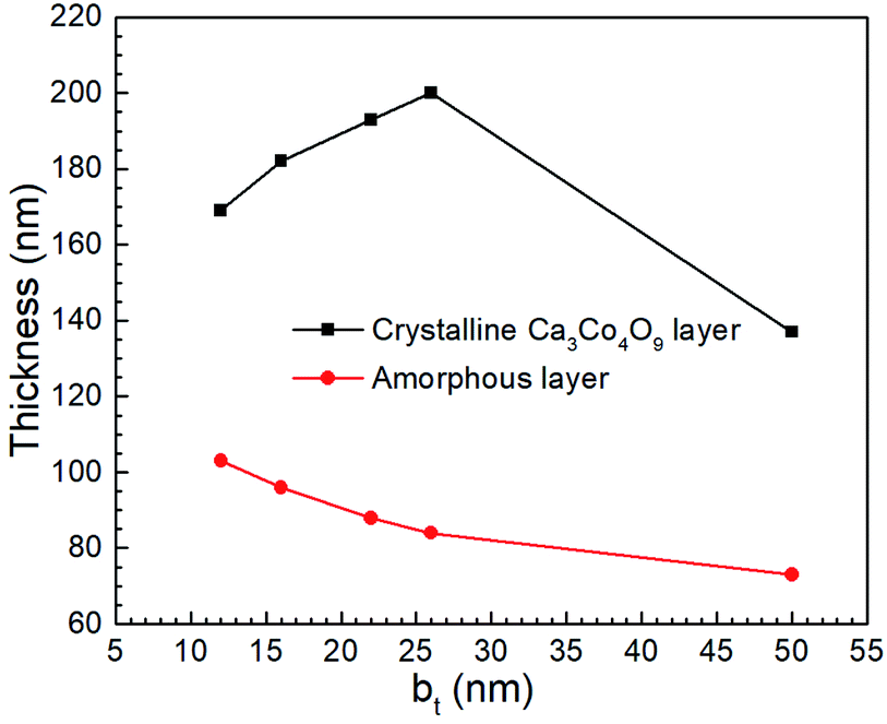 | ||
| Fig. 7 The thicknesses of crystalline Ca3Co4O9 and amorphous layers in porous films obtained by annealing Ca(OH)2/Co3O4 multilayers created from CaO/Co3O4 multilayers with 12 ≤ bt ≤ 50 nm. | ||
Thermoelectric properties
Considering that amorphous materials normally have lower electrical conductivity σ than corresponding crystalline materials and the amorphous layer has a low thermal conductivity κ, the amorphous oxide layer is assumed as an insulator. The electrical conductivity σ of Ca3Co4O9 films slightly increases with bt (Fig. 8a) and peaks around 13% porosity (Fig. 8b). For example, σ ∼ 90 S cm−1 for the film with higher porosity (13.8%) is 50% higher than for the film with lowest porosity (3.7%). But σ for the film with different porosities from 11.2 to 17.1% shows a narrow range from 80 to 95 S cm−1. The reason may be that the rough morphology and lowest quality layered structure of annealed film with bt = 12 nm cause lower carrier mobility and the high-quality layered structure of the annealed films with bt ≥ 16 nm led to high carrier mobility as shown in Fig. 4 and the size range of nanopores mainly from 120 nm to 400 nm has a slight effect for the electrical conductivity. | ||
| Fig. 8 (a) The electrical conductivity σ and the Seebeck coefficient α and (b) power factor α2σ of nanoporous Ca3Co4O9 films as function of surface porosity fraction at room temperature. | ||
The Seebeck coefficient α increases sightly with nanoporosity fraction, e.g., from α = 128 μV K−1 observed for porosity = 3.7% to α = 136 μV K−1 for porosity = 17.1%. The power factor increases from 0.96 to 1.53 μW cm−1 K−2 with increasing porosity (Fig. 8b). The highest power factor is α2σ = 1.63 μW cm−1 K−2 for the film with bt = 50 nm with highest σ.
We used 3DFEM model fitting49 to determine the effective thermal conductivity κfilm of the Ca3Co4O9 films (see Fig. 9) by using a mica substrate thermal conductivity value of κsub = 0.421 W m−1 K−1, determined by SThM probe measurements. Since κfilm depends on the thermal conductivities of the amorphous (κamorphous) and nanoporous crystalline (κnanoporous) layers, both of which are unknown, we computed κnanoporous by using a one-dimensional cross-plane thermal resistance network model for the crystalline-amorphous bilayer described by  . We selected three possible κamorphous values of 0.6, 0.8, and 1 (0.8 ± 0.2) W m−1 K−1, which are comparable to the thermal conductivity of amorphous silica.54 We assumed κamorphous to be identical in all the five samples with 50 ≥ bt ≥ 12 nm and used the measured amorphous layer thickness for each sample, i.e., 73 nm ≤ tamorphous ≤ 103 nm. This model is apt because both the amorphous and the nanoporous regions are much thinner than the ∼5 μm probe-sample heat transfer radius and have low values of fitted thermal conductivities.
 | ||
| Fig. 9 (a) Effective thermal conductivity κ film of Ca3Co4O9 films as a function of surface porosity fraction, and (b) thermal conductivity of the nanoporous crystalline Ca3Co4O9 layer κnanoporous, assuming κamorphous = 0.8 W m−1 K−1 with a ±0.2 W m−1 K−1 uncertainty captured by error bars. | ||
Plotting the effective κfilm and the values extracted for κnanoporous of the nanoporous layer as a function of porosity (see Fig. 9a and b) reveal peaks in both κfilm and κnanoporous around 13% porosity, at which σ also peaks, as shown earlier. We note that decreasing assumed κamorphous yields a higher κnanoporous. Both the κfilm and σ are low for the lowest porosity film due to the relatively higher surface roughness compared to the other films. The film with the highest porosity 17.1% (i.e., with bt = 26 nm) has the lowest κ (∼0.87 W m−1 K−1) in annealed films with bt ≥ 16 nm. The annealed film with bt = 12 nm shows low κ (∼0.8 W m−1 K−1) due to the rough morphology.
Mechanical flexibility
Surface Brillouin scattering (SBS) spectra from Ca3Co4O9 films (Fig. 10a) reveal stiffness values that are significantly lower than that of bulk Ca3Co4O9. Rayleigh peaks are seen around ± 8.5 GHz at scattering angles θs ≥ 70°. At lower scattering angles, the Rayleigh peaks merge into the central elastic peak, and we observe Sezawa peaks around ±11.5 GHz. Sezawa peaks are typical of soft films on hard substrates,55 as is our case for Ca3Co4O9 on sapphire. The invariance of the surface Rayleigh velocity with k‖d (Fig. 10b) within experimental uncertainties is indicative of the elastic properties of the Ca3Co4O9 film with negligible influence of the sapphire substrate. In contrast, the Sezawa velocity increases substantially with decreasing k‖d due to the hard sapphire substrate. We calculated the shear modulus G of the nanoporous Ca3Co4O9 film from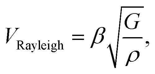 where ρ is the density and β = 0.94.56,57 Assuming isotropy, invoking E = 2G(1 + ν), using the bulk Ca3Co4O9 Poisson's ratio ν = 0.31,58 and a density ρ ∼ 3.0 g cm−3 for the nanoporous Ca3Co4O9 film determined from X-ray reflectivity measurements (ESI Fig. S3†), we get Young's and shear moduli values of G = 18.92 ± 1.14 GP, and E = 49.62 ± 2.99 GPa, respectively. Both these values for nanoporous Ca3Co4O9 film are 52.7% lower than the predicted values of G = 39.98 GPa and E = 104.86 for bulk Ca3Co4O9.58 The 21% lower density of the nanoporous Ca3Co4O9 film compared to bulk Ca3Co4O9 (3.8 g cm−3) partially explains the lower moduli. We propose that the low atomic bond density near the nanopore walls in the film also contribute to the increased mechanical compliance.
 | ||
| Fig. 10 (a) Representative Brillouin spectra from a ∼185 nm-thick nanoporous Ca3Co4O9 film (corresponding to bt = 26 nm) on sapphire for different scattering angles θs showing Rayleigh (R) and Sezawa (S) peaks. (b) Surface Rayleigh and Sezawa velocities plotted a of k‖d, where k‖ = (4πsinθs)/λ0 is the surface acoustic wave vector, and d the film thickness. | ||
Mechanical bending of the film-substrate composite showed a high retention of the electrical properties, consistent with high mechanical compliance indicated by the SBS results. Two-point resistance of the film measured as a function of bending radius rb (see Fig. 11a) showed negligible changes in the normalized resistance (ΔR/R0 ∼ 0) for rb ≥ 4 cm, where R0 is the initial resistance for each film, indicating good mechanical flexibility and low electromechanical coupling. Films synthesized from multilayers specified by bt = 12 nm and bt = 26 nm show a greater resilience to bending and bend cycling than the film corresponding to bt = 50 nm (Fig. 11b and c). While further studies are needed to understand correlations between nanoporosity, bend cycling, and mechanical compliance, our results clearly indicate that the nanoporous films are mechanically flexible and have a low electromechanical coupling for a large range of bt and bending.
 | ||
| Fig. 11 The normalized resistance changing ΔR/R0 of the Ca3Co4O9 films on mica (00l) substrates obtained by reactions of multiple stacks of Ca(OH)2/Co3O4 bilayers with 12 ≤ bt ≤ 50 nm as a function of (a) bending radius rb and (b) the number of bending cycles at a bending radius of 2 cm, and (c) after restoration to non-bent geometry. | ||
Conclusions
We have synthesized Ca3Co4O9 films with different porosities by annealing multilayers of calcium and cobalt oxide bilayers specified by Ca(OH)2/Co3O4 bilayer thicknesses bt. Increasing bt increases the nanoporosity fraction and average nanopore size in the Ca3Co4O9 film formed during annealing. The higher porosity films exhibit a 50% higher electrical conductivity as well as a high Seebeck coefficient, together with a low thermal conductivity. The nanoporous Ca3Co4O9 films show a higher mechanical compliance than the bulk Ca3Co4O9 and are resilient to mechanical bending and bend cycling. These results indicate that engineering nanoporosity in layered oxides through reactions of multilayer stacks of component oxides could be attractive for achieving mechanically-flexible high-figure-of-merit thermoelectric nanomaterials for emergent applications.Author contributions
Binbin Xin: performed experiments, data collection and analysis, writing – original draft, and writing – review & editing; Erik Ekström: magnetron sputtering; Jun Lu and Anna Elsukova: TEM data; Yueh-Ting Shih and Liping Huang: surface Brillouin scattering (SBS) spectroscopy; Yun Zhang, Wenkai Zhu, and Theodorian Borca-Tasciuc: thermal conductivity; Biplab Paul and Per Eklund: experiment design and supervision; Erik Ekström, Yueh-Ting Shih, Liping Huang, Jun Lu, Anna Elsukova, Yun Zhang, Wenkai Zhu, Theodorian Borca-Tasciuc, Ganpati Ramanath, Arnaud Le Febvrier, Biplab Paul and Per Eklund: writing – review & editing.Conflicts of interest
The authors declare no conflicts of interest.Acknowledgements
The authors acknowledge support from the Knut and Alice Wallenberg Foundation through the Wallenberg Academy Fellows program (grant no. KAW 2020.0196), the Swedish Research Council under project grant no 2021-03826, the Swedish Government Strategic Research Area in Materials Science on Functional Materials at Linköping University (Faculty Grant SFO-Mat-LiU No. 2009 00971), and the Swedish Energy Agency under project 46519-1. B. X. also acknowledges financial support from the China Scholarship Council. GR acknowledges funding from the grant CMMI 2135725 from the National Science Foundation.References
- N.-S. Choi, Z. Chen, S. A. Freunberger, X. Ji, Y. Sun, K. Amine, G. Yushin, L. F. Nazar, J. Cho and P. G. Bruce, Angew. Chem., Int. Ed., 2012, 51, 9994–10024 CrossRef CAS PubMed.
- E. Vinodkumar, M. Rotem, E. Ran, S. Gregory and A. Doron, Energy Environ. Sci., 2011, 4, 3243–3262 RSC.
- R. Tian, C. Wan, N. Hayashi, T. Aoai and K. Koumoto, MRS Bull., 2018, 43, 193–198 CrossRef CAS.
- C. S. Kim, H. M. Yang, J. Lee, G. S. Lee, H. Choi, Y. J. Kim, S. H. Lim, S. H. Cho and B. J. Cho, ACS Energy Lett., 2018, 3, 501–507 CrossRef CAS.
- Y. Du, J. Xu, B. Paul and P. Eklund, Appl. Mater. Today, 2018, 12, 366–388 CrossRef.
- B. J. Hyeong, F. Haiyu, Y. Kazuaki and S. Ali, J. Mater. Chem. C, 2015, 3, 10362–10374 RSC.
- F. J. DiSalvo, Science, 1999, 285, 703–706 CrossRef CAS PubMed.
- J. He and T. M. Tritt, Science, 2017, 357, eaak9997 CrossRef PubMed.
- A. M. Dehkordi, M. Zebarjadi, J. He and T. M. Tritt, Mater. Sci. Eng., R, 2015, 97, 1–22 CrossRef.
- D. Ni, H. Song, Y. Chen and K. Cai, Energy, 2019, 170, 53–61 CrossRef CAS.
- O. Bubnova, Z. U. Khan, A. Malti, S. Braun, M. Fahlman, M. Berggren and X. Crispin, Nat. Mater., 2011, 10, 429–433 CrossRef CAS PubMed.
- B. Olga and C. Xavier, Energy Environ. Sci., 2012, 5, 9345–9362 RSC.
- Z. Fan, D. Du, Z. Yu, P. Li, Y. Xia and J. Ouyang, ACS Appl. Mater. Interfaces, 2016, 8, 23204–23211 CrossRef CAS PubMed.
- S. Rudd, P. J. Murphy and D. R. Evans, Synth. Met., 2018, 242, 61–66 CrossRef CAS.
- H. Song, Q. Meng, Y. Lu and K. Cai, Adv. Electron. Mater., 2019, 5, 1800822 CrossRef CAS.
- Y. Akihito and T. Naoki, J. Electron. Mater., 2016, 45, 2914–2919 CrossRef.
- Y. Du, H. Li, X. Jia, Y. Dou, J. Xu and P. Eklund, Energies, 2018, 11, 2849 CrossRef.
- H. Mamur, M. R. A. Bhuiyan, F. Korkmaz and M. Nil, Renewable Sustainable Energy Rev., 2018, 82, 4159–4169 CrossRef CAS.
- Q. Jin, S. Jiang, Y. Zhao, D. Wang, J. Qiu, D. M. Tang, J. Tan, D. M. Sun, P. X. Hou, X. Q. Chen, K. Tai, N. Gao, C. Liu, H. M. Cheng and X. Jiang, Nat. Mater., 2019, 18, 62–68 CrossRef CAS PubMed.
- L.-X. Liang, Y. Deng, Y. Wang, H.-L. Gao and J. Cui, J. Nanopart. Res., 2014, 16, 1–7 CAS.
- X. Shi, H. Chen, F. Hao, R. Liu, T. Wang, P. Qiu, U. Burkhardt, Y. Grin and L. Chen, Nat. Mater., 2018, 17, 421–426 CrossRef CAS PubMed.
- J. Liang, T. Wang, P. Qiu, S. Yang, C. Ming, H. Chen, Q. Song, K. Zhao, T.-R. Wei, D. Ren, Y.-Y. Sun, X. Shi, J. He and L. Chen, Energy Environ. Sci., 2019, 12, 2983–2990 RSC.
- H. Wang, X. Liu, Z. Zhou, H. Wu, Y. Chen, B. Zhang, G. Wang, X. Zhou and G. Han, Acta Mater., 2022, 223 Search PubMed.
- R. Jayakanth, J. Mater. Res., 2016, 32, 183–203 Search PubMed.
- B. Paul, V. Khranovskyy, R. Yakimova and P. Eklund, Mater. Res. Lett., 2019, 7, 239–243 CrossRef CAS.
- D. Kenfaui, M. Gomina, J. G. Noudem and D. Chateigner, Materials, 2018, 11, 1224 CrossRef PubMed.
- P. Brinks, N. Van Nong, N. Pryds, G. Rijnders and M. Huijben, Appl. Phys. Lett., 2015, 106, 143903 CrossRef.
- S. Bresch, B. Mieller, C. Selleng, T. Stöcker, R. Moos and T. Rabe, J. Electroceram., 2018, 40, 225–234 CrossRef CAS.
- P. Wannasut, N. Keawprak, P. Jaiban and A. Watcharapasorn, IOP Conf. Ser.: Mater. Sci. Eng., 2018, 303, 012010 Search PubMed.
- B. Paul, J. L. Schroeder, S. Kerdsongpanya, N. V. Nong, N. Schell, D. Ostach, J. Lu, J. Birch and P. Eklund, Adv. Electron. Mater., 2015, 1, 1400022 CrossRef.
- M.-G. Kang, K.-H. Cho, J.-S. Kim, S. Nahm, S.-J. Yoon and C.-Y. Kang, Acta Mater., 2014, 73, 251–258 CrossRef CAS.
- M. Shikano and R. Funahashi, Appl. Phys. Lett., 2003, 82, 1851–1853 CrossRef CAS.
- M.-E. Song, H. Lee, M.-G. Kang, W. Li, D. Maurya, B. Poudel, J. Wang, M. A. Meeker, G. A. Khodaparast, S. T. Huxtable and S. Priya, ACS Omega, 2018, 3, 10798–10810 CrossRef CAS PubMed.
- J. Yu and R. Freer, J. Phys.: Energy, 2022, 4, 022001 Search PubMed.
- X. Zhu, D. Shi, S. Dou, Y. Sun, Q. Li, L. Wang, W. Li, W. Yeoh, R. Zheng and Z. Chen, Acta Mater., 2010, 58, 4281–4291 CrossRef CAS.
- E. G. Masashi Mikami and R. Funahashi, J. Mater. Res., 2005, 20, 2491–2497 CrossRef.
- J. Yu, X. Liu, W. Xiong, B. Wang, M. J. Reece and R. Freer, J. Alloys Compd., 2022, 902 Search PubMed.
- B. Paul, Y. Zhang, W. Zhu, B. Xin, G. Ramanath, T. Borca-Tasciuc and P. Eklund, Appl. Phys. Lett., 2022, 120, 061904 CrossRef CAS.
- B. Xu, T. Feng, M. T. Agne, L. Zhou, X. Ruan, G. J. Snyder and Y. Wu, Angew. Chem., Int. Ed., 2017, 56, 3546–3551 CrossRef CAS PubMed.
- B. Paul, E. M. Björk, A. Kumar, J. Lu and P. Eklund, ACS Appl. Energy Mater., 2018, 1, 2261–2268 CrossRef CAS PubMed.
- B. Paul, J. Lu and P. Eklund, ACS Appl. Mater. Interfaces, 2017, 9, 25308–25316 CrossRef CAS PubMed.
- Y. Yin and A. Tiwari, Sci. Rep., 2021, 11, 6324 CrossRef CAS PubMed.
- U. Hira, S. S. Ali, S. Latif, N. Pryds and F. Sher, ACS Omega, 2022, 7, 6579–6590 CrossRef CAS PubMed.
- J. Yu, M. Nelo, X. Liu, S. Shao, B. Wang, S. J. Haigh, H. Jantunen and R. Freer, J. Eur. Ceram. Soc., 2022, 42, 3920–3928 CrossRef CAS.
- B. Xin, A. L. Febvrier, R. Shu, A. Elsukova, V. Venkataramani, Y. Shi, G. Ramanath, B. Paul and P. Eklund, ACS Appl. Nano Mater., 2021, 4, 9904–9911 CrossRef CAS.
- R. Teotia, S. K. Verma, D. Kalita, A. K. Singh, G. Dahe and J. Bellare, J. Mater. Sci., 2017, 52, 12513–12523 CrossRef CAS.
- M. U. H. Joardder, C. Kumar, R. J. Brown and M. A. Karim, J. Food Eng., 2015, 166, 156–164 CrossRef CAS.
- B. Xin, A. L. Febvrier, L. Wang, N. Solin, B. Paul and P. Eklund, Mater. Des., 2021, 210, 110033 CrossRef CAS.
- Y. Zhang, W. Zhu and T. Borca-Tasciuc, Nanoscale Adv., 2021, 3, 692–702 RSC.
- Y. Zhang, W. Zhu, L. Han and T. Borca-Tasciuc, Rev. Sci. Instrum., 2020, 91, 014901 CrossRef CAS PubMed.
- Y. Zhang, W. Zhu, F. Hui, M. Lanza, T. Borca-Tasciuc and M. Muñoz Rojo, Adv. Funct. Mater., 2019, 30, 1900892 CrossRef.
- Y. Zhang, W. Zhu and T. Borca-Tasciuc, Oxf. Open Mater. Sci., 2021, 1, itab011 CrossRef.
- G. Michael and H. Liping, J. Phys. D: Appl. Phys., 2012, 45, 275302 CrossRef.
- D. G. Cahill and R. O. Pohl, Phys. Rev. B: Condens. Matter Mater. Phys., 1987, 35, 4067–4073 CrossRef CAS PubMed.
- C. Sumanya, J. D. Comins and A. G. Every, Wave Motion, 2017, 68, 78–87 CrossRef.
- B. D. Ozsdolay, X. Shen, K. Balasubramanian, G. Scannell, L. Huang, M. Yamaguchi and D. Gall, Surf. Coat. Technol., 2017, 325, 572–578 CrossRef CAS.
- G. Carlotti, Appl. Sci., 2018, 8, 124 CrossRef.
- A. Jain, S. P. Ong, G. Hautier, W. Chen, W. D. Richards, S. Dacek, S. Cholia, D. Gunter, D. Skinner, G. Ceder and K. A. Persson, APL Mater., 2013, 1, 011002 CrossRef.
Footnote |
| † Electronic supplementary information (ESI) available. See https://doi.org/10.1039/d2na00278g |
| This journal is © The Royal Society of Chemistry 2022 |