
 Open Access Article
 This Open Access Article is licensed under a Creative Commons Attribution-Non Commercial 3.0 Unported Licence
Realization of a multi-band terahertz metamaterial absorber using two identical split rings having opposite opening directions connected by a rectangular patch
Ben-Xin
Wang
 *,
Wei
Xu
,
Yangkuan
Wu
,
Zhuchuang
Yang
,
Shengxiong
Lai
and
Liming
Lu
*,
Wei
Xu
,
Yangkuan
Wu
,
Zhuchuang
Yang
,
Shengxiong
Lai
and
Liming
Lu
School of Science, Jiangnan University, Wuxi, 214122, China. E-mail: wangbenxin@jiangnan.edu.cn
First published on 14th January 2022
Abstract
A multi-band metamaterial absorber in the terahertz regime using a periodically arranged surface structure placed on an ultra-thin insulating dielectric slab backed by a metallic ground plane is demonstrated in this paper. Its surface structure consists of two identical split rings having opposite opening directions connected by a rectangular patch. The surface structure can have a strong electromagnetic interaction with incident terahertz waves, thereby generating two localized resonance absorption peaks with different frequencies, and the superposition effect of these two absorption peaks gives rise to dual-band absorption. With the aid of the near-field distributions of the two absorption peaks, the physical mechanism of the dual-band absorption is revealed. The dimension changes of the surface structure, including the split rings and the rectangular patch, play a key role in controlling and adjusting the resonance performance of dual-band absorption. Further optimization of the surface structure without increasing the number of sub-resonators provides the ability to increase the number of absorption peaks, which is different from prior multi-band absorption devices that typically require more sub-resonators in their surface structures. Multi-band metamaterial absorbers designed in this paper should have great application prospects in the field of terahertz absorption.
Introduction
Metamaterial absorbers, as an important branch of metamaterial resonant devices, have attracted extensive research interest due to their series of excellent electromagnetic properties, including near-perfect absorption, ultra-thin dielectric layer thickness, and flexible expansion of the absorption bandwidth.1–3 Compared with the large and bulk thickness of traditional absorbers, such as Salisbury screens4 and Jaumann absorbers,5 the thickness of metamaterial absorbers, especially the thickness of their middle dielectric layer, is only a few tenths or even one hundredth of the resonance wavelength, which makes metamaterial absorbers have the advantages of light weight and easy construction.1–3 The first metamaterial absorber operating in the microwave region using the sandwich structure of an electric metallic split ring and lossy dielectric and metallic cut wire was reported.6 In this structure, the simultaneous suppression of transmission and reflection provides the ability to realize near-perfect absorption.6Since then, many types of metamaterial absorbers have been widely presented, and their operating frequencies are not limited to microwaves but gradually expanded to all frequency ranges related to technology. For example, a metamaterial absorber using an array of metallic split rings placed on a metallic ground plane separated by a dielectric spacer in the frequency range of 0.8–1.8 THz was demonstrated.7 A patch-antenna-based surface structure was presented to achieve near-unity absorption in the optical region.8 Mid-infrared reconfigurable metamaterial absorbers developed by employing different surface structure designs were suggested to achieve large absorption.9 A metamaterial absorber operating in the radio band (30–300 MHz) was designed and demonstrated, whose surface structure is a square patch with a circular cutout in the center and four semi-circular cutouts in the center of each side.10 These demonstrated metamaterial absorbers are promising for a wide range of applications in terms of thermal imaging, bolometers, optical switches, refractive index sensors, solar cells, stealth technology, and so on.1–3 Note that, however, these metamaterial absorbers usually exhibit single-band absorption, which greatly limits their application prospects.
To broaden the application potential of metamaterial absorbers, an extended research direction in this field is simultaneously achieving near-perfect absorption in multiple frequency bands (or multi-band absorption) in a selected spectral range. Therefore, many efforts have been proposed to achieve multi-band absorption. For instance, a kind of dual-band metamaterial absorber in the terahertz region based on a multi-layer structure of graphene/MgF2 placed on a continuous metallic plane was theoretically designed to achieve the dual-band near-perfect absorption effect.11 It should be noted that when the number of stacked layers is less than eight, the designed structure does not support the dual-band absorption effect.11 Two pairs of circular-patterned metal–dielectric stacks were employed to excite the dual-band absorption peaks in the mid-infrared frequency regime, and the absorption peak position could be adjusted by the dielectric constant of the dielectric spacer.12 A stacked structure design consisting of periodic SiO2 ribbons, mono-layer graphene, a polymide layer, and a terahertz cold mirror formed by alternate stacking of Si and Al2O3 was demonstrated to realize tunable dual-band absorption.13 Although these stacked design methods can achieve nearly perfect absorption of incident electromagnetic waves, these structures themselves have many disadvantages, such as complex structure design and time-consuming structure optimization.11–16 More importantly, these stacked layers need to be accurately aligned; otherwise the designed resonant structures cannot support multi-band absorption.
To overcome the issues encountered by the stacking method, the coplanar design strategy, in which multiple sub-resonators having different dimensions or shapes are arranged on a plane, is widely utilized to achieve multi-band absorption.17–23 For example, a dual-band terahertz metamaterial absorber using four periodically patterned elliptical graphene nanodisks as the surface structure of the absorption device was proposed. The absorption peak position of the dual-band metamaterial absorber can be modulated by varying the conductivity of graphene via a bias or chemical doping.17 A dual-band perfect metamaterial absorber using a surface structure of five graphene disks, one larger surrounded by four smaller, was proposed in the terahertz region. The metamaterial absorber can have selective frequency tunability and it can tune each resonance peak independently by controlling the conductivity of graphene.18 A dual-band polarization independence terahertz metamaterial absorber using four arranged T-shape graphene resonators was presented.19 Furthermore, to obtain more absorption peaks, such as triple-band absorption, it is usually necessary to place or arrange more sub-resonators in the coplanar structure (or the surface structure).19–23
However, placing a large number of sub-resonators in a coplanar structure (or a surface structure) usually results in large-scale unit dimensions, which are not in line with the design trend of miniaturization and compactness. More importantly, as the number of absorption peaks increases, the coplanar structure (or the surface structure) itself becomes very complex, which inevitably leads to strong interactions between these sub-resonators, thereby reducing or decreasing the overall absorption strength of multi-band absorption devices. Therefore, it is still an important issue in the field of metamaterials to realize multi-band absorption with high performance to deal with various applications.
In this paper, we suggest a class of multi-band terahertz metamaterial absorbers composed of a metallic surface structure and a dielectric spacer on top of a continuous metallic ground plane. The surface structure of the multi-band absorption device consists of two identical split rings having opposite opening directions connected by a rectangular patch. The suggested structure can strongly interact with the incident beam to excite two discrete terahertz absorption peaks, thereby obtaining the dual-band terahertz absorption effect. The physical origin of the dual-band absorption is discussed with the aid of the near-field distributions of the two discrete terahertz absorption peaks, and it is revealed that the superposition effect of two localized resonance responses with different formation causes on the surface structure leads to the dual-band absorption. The influence of parameter changes of the surface structure (including two split rings and the rectangular patch) on the absorption response of the suggested metamaterial absorber is also discussed. The results show that the changes in the surface structure parameters can not only significantly control the absorption performance of the metamaterial absorber, but also adjust the number of absorption peaks. This is obviously different from the multi-band absorbers reported at this stage, in which the increase in the number of absorption peaks is achieved at the expense of a large number of sub-resonators or the complexity of the surface structure.19–23 The multi-band metamaterial absorber designed here should have broad application prospects in terahertz absorption, terahertz filtering, terahertz sensing, etc.
Structure design and model
The basic cell of the suggested multi-band metamaterial absorber is composed of a metallic surface structure, a dielectric separation layer and a continuous metallic plane, and its three-dimensional schematic diagram is illustrated in Fig. 1(a). The surface structure of the multi-band metamaterial absorber consists of two identical split ring resonators (SRRs) having opposite opening directions, and the two SRRs are connected with a rectangular patch, see Fig. 1(b). The two identical SRRs have a baseline length of l2 = l3 = 100 μm, arm length of w2 = w3 = 40 μm and line width of w = 5 μm. The length and width of the rectangular patch connecting the two SRRs are l1 = 40 μm and w1 = 80 μm, respectively. The dielectric separation layer has a thickness of t = 15 μm, which is approximately 1/33 of the resonance wavelength of the first absorption peak (at 0.61 THz) or 1/12 of the resonance wavelength of the second absorption peak (at 1.68 THz). This indicates that the thickness of the dielectric separation layer used here can be considered to belong to the ultra-thin category. The dielectric separation layer is a lossy material; polyimide can be used in actual manufacturing, and its dielectric constant is set to 3(1 + i0.06).24,25 The basic unit of the multi-band metamaterial absorber has the same dimension or period on the x-axis and y-axis, and here they are set as a = b = 120 μm. | ||
| Fig. 1 (a) Three dimensional schematic diagram of the unit cell of the multi-band terahertz metamaterial absorber; (b) two dimensional schematic diagram of the unit cell of the multi-band terahertz metamaterial absorber. | ||
The simulation results of the manuscript are based on FDTD Solutions (Lumerical, Version 8.6) using the algorithm of finite-difference time-domain. In the simulation code, a beam of a plane electromagnetic wave having the frequency range of (0.5–2.0) THz irradiates the structure of the suggested metamaterial absorber vertically. Without a special statement, the electric field of the plane wave is always along the x-axis direction, which is the baseline direction of the SRRs. In order to theoretically construct an infinite array of cells, periodic boundary conditions are used along the x-axis and y-axis, and perfectly matched layers in the direction of light propagation are applied to eliminate the influence of unnecessary scattering on the absorption performance of the resonant device. The surface structure and the continuous metallic plane are both made from gold, which has a conductivity of 4.09 × 10⁷ S m−1, and the selection of gold is mainly due to its excellent characteristics, including high temperature resistance, high conductivity and oxidation resistance, compared with other metal materials such as Ag, Al, etc. Since the thickness of the continuous gold plane is greater than the skin depth of the incident plane wave, the transmission of the structure of the suggested metamaterial absorber is approximately zero. The reflection of the absorber structure can also be approximately equal to zero by adjusting the impedance of the designed metamaterial structure so that its impedance is equivalent to the impedance of air. Simultaneously suppressed (or extremely low) transmission and reflection provide the possibility for successful realization of near-perfect absorption.
Because multi-band metamaterial absorbers are quite ideal in many practical applications in terms of explosive material detection, spectral imaging, and sensing,1–3 the research of multi-band metamaterial absorbers has become a hotspot, and many efforts have been devoted to their development in recent years.11–23 Therefore, the focus of this manuscript mainly involves the design and research of a multi-band metamaterial absorber. Although high-Q and broadband metamaterial absorbers have many special applications,26–28 this manuscript does not involve relevant research. In the following work, our research group will try research on high-Q and broadband absorption.
Generally speaking, dedicated to the vigorous development of multi-band metamaterial absorbers, researchers have gradually proposed and developed two common design methods of coplanar and stacking to realize multi-band absorption.11–23 However, compared with previously reported multi-band metamaterial absorbers,11–23 the multi-band metamaterial absorber designed here should have the following advantages. Firstly, the absorption mechanism of the manuscript is different from previous ones. The coupling effect of the localized resonance responses of two identical split rings and the rectangular patch connecting them results in dual-band and even triple-band absorption, which is different from the operating mechanism of previous metamaterial absorbers that merely employ the superposition effect of sub-resonator resonance modes.11–23 In other words, this manuscript expands the mechanism diversity of multi-band metamaterial absorbers to a great extent. Secondly, this manuscript has more advantages in controlling the number of absorption peaks. As illustrated in Fig. 6, the increase of the offset (δ) of the rectangular patch provides the possibility of realizing more absorption peaks, while keeping the lattice period and thickness of the dielectric layer unchanged. It should be noted that it is rather difficult to expand the number of absorption peaks if there are no other significant changes in previously reported metamaterial absorbers.11–23 This is mainly because the expansion of the number of their absorption peaks is usually achieved by sacrificing the number of sub-resonators (or increasing the lattice period) or increasing the thickness of the dielectric layer (or increasing the stacking layers).11–23 Thirdly, although our research group is unable to fabricate the designed metamaterial absorber based on metal–dielectric-metal due to the lack of experimental facilities and experimental experience, the multi-band metamaterial absorber designed here should have obvious merits of easy fabrication and low construction cost compared with previously reported absorbers, in particular graphene-based absorbers in recent five years. As we all know, it is quite difficult to fabricate graphene patterned structures (especially those graphene absorber structures with complex patterns or multi-layer stacking), but it is rather easy to construct metal patterned metamaterials by using the existing mature etching and lithography technologies. Fourthly, this manuscript has more freedom or flexibility in the modulation of absorption performance. As shown in Fig. 4 and 7, the two absorption peaks can be simultaneous modulated and the number of absorption peaks can even be increased via changing the dimensions of the absorber structure. However, previously reported metamaterial absorbers usually cannot do this because changing or regulating the sizes of sub-resonators can only regulate the performance of their corresponding absorption peak, while the resonance characteristics of other absorption peaks remain unchanged.11–23
Results and discussion
The absorption spectrum of the suggested metamaterial absorber in the frequency range of interest, 0.5–2.0 THz, is given, see Fig. 2(a). Two absorption peaks with very large absorbance are found in this absorption spectrum, and the combination of two discrete and high absorbance peaks achieves dual-band absorption. In order to facilitate the subsequent discussion, the two absorption peaks are marked with different symbols, where the low-frequency absorption peak is marked as Peak A, while the high-frequency absorption peak is marked as Peak B. Peak A has a frequency of 0.61 THz with an absorbance of 98.75%, Peak B having an absorbance of 99.46% is resonated at 1.68 THz, and the average absorbance of the two absorption peaks is 99.11%, thus achieving a nearly perfect absorption effect. It should be noted that due to the anti-symmetric surface structure design, the absorption performance designed here should show a dependence sensitive to the polarization angle, and we have made many structure attempts to obtain polarization-insensitive absorption properties, but the results are not very ideal. But in fact, for some applications, such as controlling thermal emissivity29 and polarization detectors,30 polarization-sensitive absorbers may have more advantages than polarization-insensitive absorbers.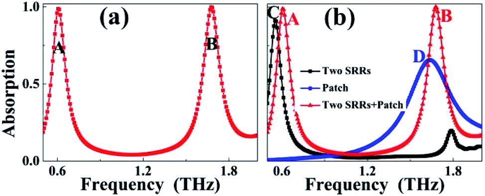 | ||
| Fig. 2 (a) Absorption response of the multi-band terahertz metamaterial absorber; (b) comparison of absorption responses among the SRR absorber, patch absorber, and designed multi-band absorber. | ||
In order to preliminarily explore and investigate the physical mechanism of the dual-band metamaterial absorber, two reduced metamaterial absorber structures are designed. The surface structures of the two reduced metamaterial absorbers are formed by two identical SRRs (called the SRR absorbers) and a rectangular patch (called the patch absorber), respectively. The difference between the two reduced metamaterial absorbers is only in the surface structure, while the structure parameters of the other parts of the two reduced metamaterial absorbers are consistent with those of the dual-band metamaterial absorber presented in Fig. 1. The comparative absorption spectra of the two reduced metamaterial absorbers and the dual-band metamaterial absorber are given in Fig. 2(b). As shown, the SRR absorber exhibits the single-band absorption effect, and its resonance frequency and absorbance are 0.55 THz and 91.21%, respectively. The patch absorber also exhibits the single-band absorption effect with a resonance frequency of 1.64 THz, but its absorbance is quite low, only 65.61%. By comparing the absorption spectra of these two reduced metamaterial absorbers with the absorption spectrum of the dual-band metamaterial absorber, it can be seen that the positions and absorbance of the two absorption peaks of the dual-band metamaterial absorber are both different from those of the two reduced metamaterial absorbers, which reveals that the formation mechanism of the dual-band metamaterial absorber is not merely derived from the superimposition effect of the two reduced absorber structures. A large amount of literature shows that previously designed multi-band metamaterial absorbers usually originate from the superimposition effect of the absorption peak corresponding to each specific sub-resonator. However, different from this mechanism, the physical origin of the dual-band metamaterial absorber designed here should be derived from the coupling effect of the two SRRs and rectangular patch connecting them.
In order to understand the physical mechanism of the dual-band metamaterial absorber more clearly and intuitively, we provide the near-field patterns of Peak A and Peak B at the central plane of the surface structure. As observed in Fig. 3, the near-field patterns of these two absorption peaks are both concentrated on the edges of the surface structure, including the edges of the two SRRs and the edges of the rectangular patch, resulting in localized resonance effects and modes. In other words, the two absorption peaks of the dual-band metamaterial absorber should be resulted from the localized resonance effects of the surface structure. However, for each specific absorption peak, its near-field local position or near-field enhancement area is different. For example, for Peak A, its electric field |E| is mainly focused on the arms of the two SRRs, see Fig. 3(a). In particular, the field enhancement intensities of the two arms on the left and the two arms on the right are the same, or the field distributions on the left and right arms are symmetrical about the center of the surface structure. We further found in Fig. 3(b) that the Ez fields of peak A also have the symmetrical distribution feature, except that the charge properties on the left and right sides or arms are opposite. It should be noted that the field enhancement effects of the edges of the rectangular patch connecting the two SRRs, in Fig. 3(a) and (b), are both quite low. This indicates that this absorption mode is mainly derived from the localized resonance response of the two SRRs. According to the field concentration characteristics of Peak A in Fig. 3(a) and (b), we can infer that Peak A should be caused by the combined effect of LC resonance (or fundamental response) of the two SRRs.31–33 Actually, some early terahertz metamaterial studies also discussed the fundamental mode or LC mode of resonant structures.34–39
 | ||
| Fig. 3 (a) Electric field |E| distribution of Peak A at the central plane of the surface structure; (b) electric field Ez distribution of Peak A at the central plane of the surface structure; (c) electric field |E| distribution of Peak B at the central plane of the surface structure; (d) electric field Ez distribution of Peak B at the central plane of the surface structure. | ||
Different from the near-field pattern of Peak A, the near-field distribution of Peak B is concentrated on not only the arms of the two SRRs, but also the edges of the rectangular patch, see Fig. 3(c) and (d), which reveals that the synergy of the localized resonance effect of the two SRRs and the localized resonance effect of the rectangular patch leads to the formation of Peak B. As revealed in Fig. 3(c), the electric field concentration position and intensity on the left and right arms of the two SRRs are the same, and the electric field distribution on both sides of the rectangular patch is also the same, thus presenting the characteristics of symmetrical field distribution. But please note that the charge properties of the left and right arms of the two SRRs are opposite, and the charge properties of both sides of the rectangular patch are also opposite, see Fig. 3(d). According to the near-field pattern characteristics of Fig. 3(a) and (b), it can be seen that the LC resonance effect or fundamental resonance effect is excited on the two SRRs, while the dipole resonance effect can be induced on the rectangular patch. The coordination effect of the LC resonance of the two SRRs and the dipole resonance of the rectangular patch produces Peak B.
We next explore the influence of dimension changes of the surface structure of the dual-band metamaterial absorber on the absorption performance of the suggested absorption device and look forward to further confirming the formation mechanism of the two absorption peaks. Fig. 4(a) and (b) show the influence of changes in the length l1 and width w1 of the rectangular patch on the absorption spectrum of the dual-band metamaterial absorber, respectively. As observed, the dimension variations of the rectangular patch play an important role in controlling the resonance frequencies of the dual-band metamaterial absorber, while the change in absorbance is quite weak. Note, however, that the dimension of the rectangular patch has a different frequency change rate for each absorption peak. It is found that the frequency change speed (or movement amount) of Peak B with the variation of length (l1) of the rectangular patch is larger than that of Peak A. The control of the absorption spectrum of the dual-band metamaterial absorber can also be gained by modifying the dimensions of the two SRRs. It can be seen from Fig. 4(c) and (d) that the frequency change speed (or the amount of movement) of Peak A and Peak B is roughly the same when the baseline (or the arm length) of the two SRRs changes simultaneously. These results demonstrate that the frequencies of the two absorption peaks can be adjusted by controlling the dimensions of the two SRRs or the dimensions of the rectangular patch, thus confirming that the two absorption peaks should be due to the coordination effect of the localized resonance effects of the two SRRs and rectangular patch.
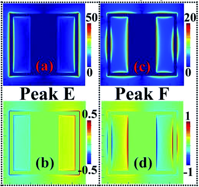
Note that when the arm lengths (w2) of the two SRRs are both equal to 45 μm, the two SRRs will be connected by their arms to form a closed-ring structure, and then the surface structure of the suggested metamaterial absorber becomes a closed-ring resonator and an embedded rectangular patch. In this case, its absorption spectrum is shown in the black curve of Fig. 4(d). As given, two absorption peaks with an average absorbance of 95.02% are realized. The absorption peak with a low frequency of 0.73 THz is marked as Peak E, while the absorption peak with a high frequency of 1.77 THz is marked as Peak F. The near-field patterns of these two absorption peaks are given to analyze their formation mechanism. As shown in Fig. 5(a) and (b), the near-field patterns of Peak E are chiefly concentrated on the left and right sides of the closed-ring resonator. Their near-field concentration intensity on both sides of the closed-ring resonator is the same, and the only difference is that their charge properties are opposite, see Fig. 5(b). These near-field distribution features reveal that Peak E is caused by the dipole resonance effect of the closed-ring resonator. Different from the case of Peak E, Peak F should be originated from the synergy of the dipole resonance of the closed-ring resonator and the dipole resonance of the rectangular patch because of the following reasons. Firstly, the near-field distributions of this mode are not only symmetrically focused on both sides of the closed-ring resonator but also symmetrically focused on both sides of the rectangular patch, see Fig. 5(c) and (d). Secondly, the charge properties gathered on both sides of the closed-ring resonator and rectangular patch are opposite.
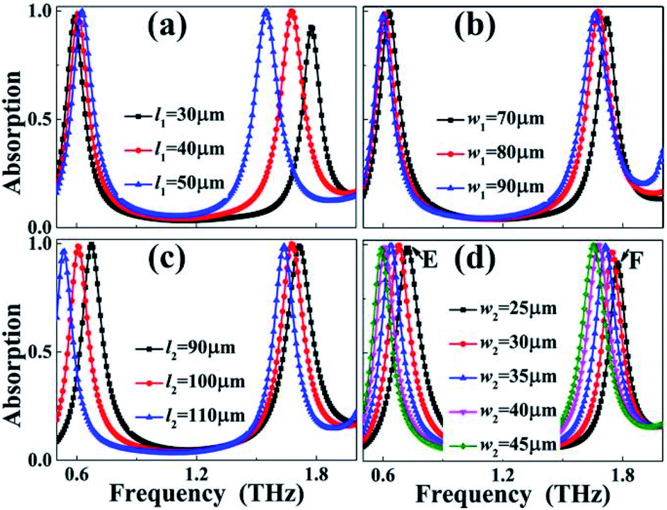 | ||
| Fig. 4 (a) Absorption response of the multi-band terahertz metamaterial absorber with length (l1) changes of the rectangular patch; (b) absorption response of the multi-band terahertz metamaterial absorber with width (w1) changes of the rectangular patch; (c) absorption response of the multi-band terahertz metamaterial absorber with baseline length (l2 = l3) changes of the two SRRs; (d) absorption response of the multi-band terahertz metamaterial absorber with the arm length (w2 = w3) changes of the two SRRs. | ||
 | ||
| Fig. 5 (a) Absorption response of the multi-band terahertz metamaterial absorber with length (l1) changes of the rectangular patch; (b) absorption response of the multi-band terahertz metamaterial absorber with width (w1) changes of the rectangular patch; (c) absorption response of the multi-band terahertz metamaterial absorber with baseline length (l2 = l3) changes of the two SRRs; (d) absorption response of the multi-band terahertz metamaterial absorber with the arm length (w2 = w3) changes of the two SRRs. | ||
We further study the influence of the offset of the rectangular patch along the positive x-axis on the absorption response of the suggested dual-band metamaterial absorber. The offset along the positive x-axis is expressed by the symbol δ. It should be noted that moving along the positive or negative x-axis has the same effect on the resonance performance. The simulation results in Fig. 6(a) demonstrated that the offset of the rectangular patch (or the size of δ) plays an important role in controlling the resonance performance of the suggested dual-band metamaterial absorber, including absorbance, absorption frequency and even the number of absorption peaks, which is much extensive and complex than the modulation of absorption frequency and intensity by changing the dimensions of two SRRs (or rectangular patch). As a typical example, when the δ is 25 μm, the rectangular patch will be connected to the right arms of the two SRRs to form a connected (or composite) surface structure. In this case, three absorption peaks with an average absorbance of 97.14% can be obtained, see the red curve of Fig. 6(a). The first absorption peak (marked as Peak G) has a frequency of 0.57 THz, while the last two absorption peaks having the frequencies of 1.42 THz (marked as Peak H) and 1.61 THz (marked as Peak I) can be gained, respectively. According to the near-field patterns of these three absorption peaks, it can be clearly seen that when the right arms of the two SRR are connected to the rectangular patch, their electric fields become quite complicated compared to the field distributions in Fig. 3 and 5. It is found in Fig. 6(b)–(d) that the electric field corresponding to each absorption peak occupies a specific area or position on the connected (or composite) surface structure, and the superposition effects of three absorption peaks occupying different localized positions lead to triple-band absorption.
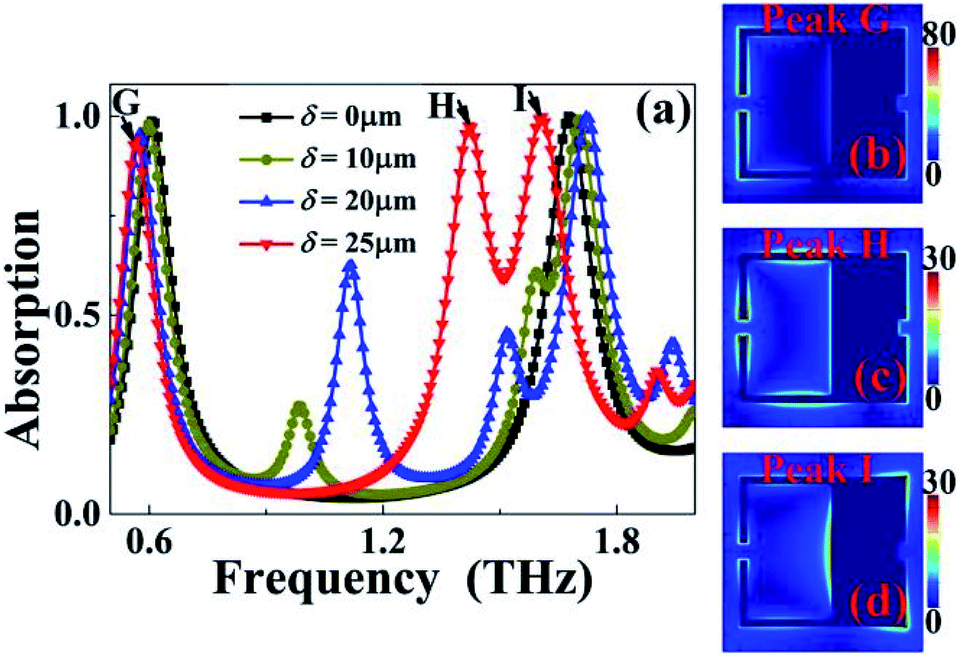 | ||
| Fig. 6 (a) Absorption response of the multi-band terahertz metamaterial absorber with the offset (δ) changes of the rectangular patch along the positive x-axis; (b) electric field |E| distribution of Peak G at the central plane of the surface structure; (c) electric field |E| distribution of Peak H at the central plane of the surface structure; (d) electric field |E| distribution of Peak I at the central plane of the surface structure. | ||
On the basis of the surface structure of the suggested dual-band metamaterial absorber, further dimension optimization of its surface structure can also achieve triple-band absorption. Here, we only change the arm lengths of one of the two SRRs to reduce the w3 = 20 μm, while keeping the other structure dimensions unchanged, including the rectangular patch parameters, the sizes of the other SRR, the properties of the dielectric layer, the simulation code, etc. The triple-band absorption effect can be achieved through slight optimization of the surface structure. The schematic diagram of the optimized surface structure is shown in Fig. 7(a), and the corresponding absorption curve is illustrated in Fig. 7(b). According to this absorption curve, three discrete absorption peaks with large absorbance can be easily found, thereby achieving the so-called triple-band absorption. The three absorption peaks are marked as Peak J, Peak K, and Peak L from low to high according to their resonance frequencies.
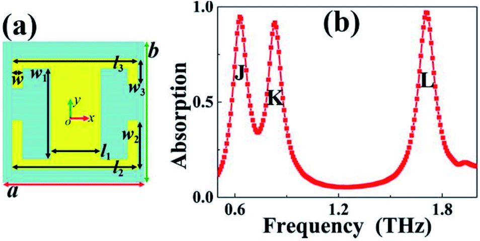 | ||
| Fig. 7 (a) Two dimensional schematic diagram of the unit cell of the re-optimized multi-band terahertz metamaterial absorber; (b) absorption response of the re-optimized multi-band terahertz metamaterial absorber. | ||
With the help of the near-field patterns of Peak A, Peak B, and Peak C, their formation mechanisms are discussed. As presented in Fig. 8(a) and (b), the near-field patterns of Peak J are symmetrically gathered on the arms of the bottom SRR, while the field distributions of the other parts of the surface structure, including the top SRR and the rectangular patch, can be ignored. Fig. 8(b) further reveals that the two arms of the bottom SRR have opposite charge properties. In accordance with the near-field patterns of Peak J, this absorption mode should be mainly attributed to the LC resonance response or fundamental resonance effect of the bottom SRR. Because the near-field pattern of Peak K at the top SRR and the near-field enhancement of Peak J at the bottom SRR have similar distribution characteristics, their differences lie only in the gathering position or area of the near-field, especially on different SRRs, see Fig. 8(c) and (d). Therefore, it can be deduced that the formation mechanism of Peak K mainly comes from the LC resonance response or fundamental resonance effect of the top SRR. Different from Peak J and Peak K, we observed that the near-field patterns of Peak L are concentrated not only on the arms of the top and bottom SRRs, but also on the both sides of the rectangular patch connecting the two SRRs, see Fig. 8(e) and (f). Meanwhile, the charge properties of Peak L of Fig. 8(f) at the two arms of the top SRR, two arms of the bottom SRR, and both sides of the rectangular patch are all opposite. This reveals that the synergy of the LC resonance response of the top SRR, the LC resonance response of the bottom SRR, and the dipole resonance response of the rectangular patch induces Peak L.
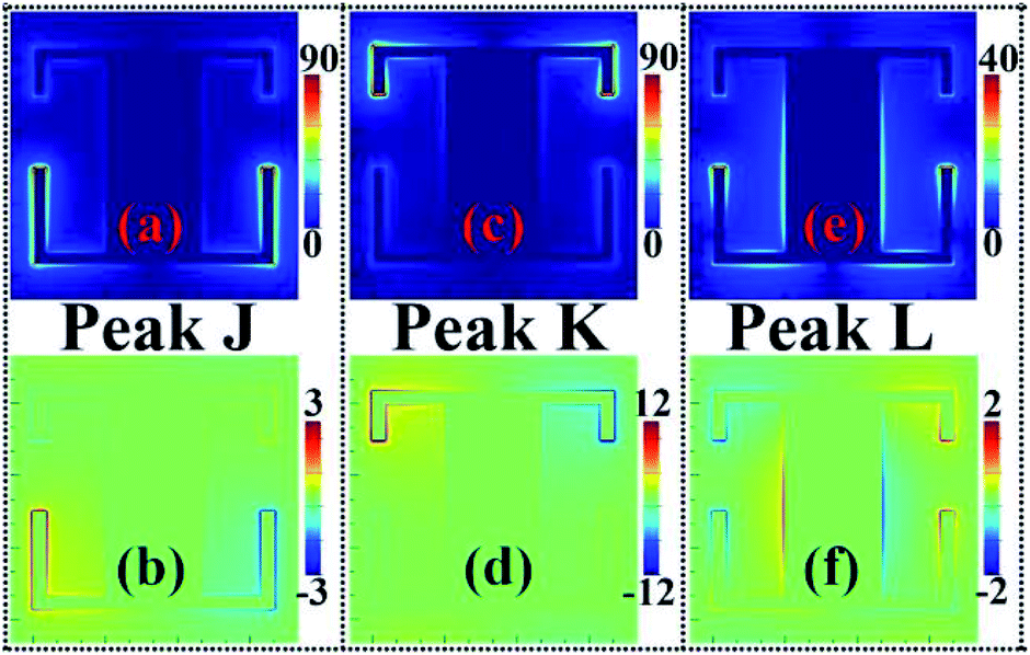 | ||
| Fig. 8 (a) Electric field |E| distribution of Peak J at the central plane of the surface structure; (b) electric field Ez distribution of Peak J at the central plane of the surface structure; (c) electric field |E| distribution of Peak K at the central plane of the surface structure; (d) electric field Ez distribution of Peak K at the central plane of the surface structure; (e) electric field |E| distribution of Peak L at the central plane of the surface structure; (f) electric field Ez distribution of Peak L at the central plane of the surface structure. | ||
Due to the lack of experimental facilities and experience, it is rather difficult for us to experimentally verify the designed metamaterial absorber at this stage. However, the structure designed here could be realized by the construction processes shown in Fig. 9. The experimental construction processes can be roughly divided into the following steps.40–42 Firstly, an Au film larger than the skin depth of the incident beam could be uniformly evaporated on the surface of the supporting material (such as silica or silicon); secondly, the dielectric material (such as polyimide) with an optimized thickness could be evenly spin coated on the Au film to act as the middle dielectric layer of the metamaterial absorber; thirdly, for the top Au patterned array, the technologies of spin-coating, exposure, development, evaporation, and lift-off could be used to transfer it onto the middle dielectric layer. Through the above steps, the metamaterial absorber could be constructed.40–42
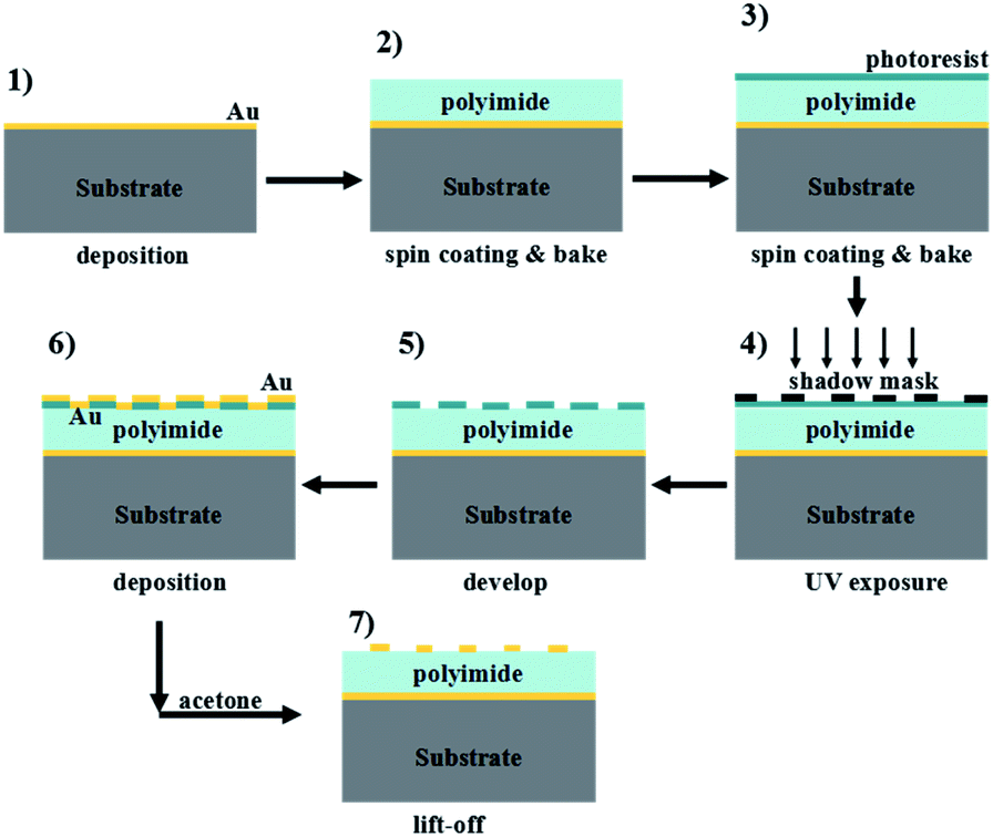 | ||
| Fig. 9 Schematic diagram of the possible construction steps of the designed metamaterial absorber. | ||
Conclusions
A multi-band metamaterial absorber operating in the terahertz range using a metallic surface structure and a metallic ground separated by an ultra-thin dielectric spacer is proposed and investigated in this paper. Two identical split ring resonators with opposite opening directions are connected by a rectangular patch to form the surface structure of the multi-band absorber. When the incident terahertz wave irradiates the metamaterial absorber, its surface structure exhibits an obvious interaction with the incident beam, thereby exciting two localized resonance modes with different frequencies but large absorbance, and the superposition of the two localized resonance modes results in dual-band absorption. The physical mechanism of the dual-band terahertz metamaterial absorber can be better analyzed with the aid of the near-field distribution of each absorption peak. The influence of parameter changes of the two split ring resonators as well as the parameter variations of the rectangular patch connecting them on the dual-band absorption performance has been studied and discussed. The results of the study found that in addition to the control of the absorption frequencies of the dual-band terahertz metamaterial absorber by these structure parameter changes, an absorber with a larger number of absorption peaks can also be achieved through parameter adjustment or optimization. Taking into account this absorption feature, two kinds of structure re-optimization designs are demonstrated to realize near perfect absorption at three discrete frequencies. The formation mechanism of these two triple-band terahertz metamaterial absorbers obtained through structure re-optimization is also discussed with the help of near-field distributions. This study should be available for useful guidelines for future research on multi-band metamaterial absorbers and their potential applications.Author contributions
Ben-Xin Wang: conceptualization, data curation, formal analysis, funding acquisition, project administration, and writing – review & editing; Wei Xu: data curation, investigation, validation, resources, and writing – original draft; Yangkuan Wu: data curation, formal analysis, and validation; Zhuchuang Yang: data curation, methodology, and validation; Shengxiong Lai: data curation, methodology, and validation; Liming Lu: data curation and validation.Conflicts of interest
There are no conflicts to declare.Acknowledgements
This work was supported by the National Natural Science Foundation of China (62105128 and 11647143) and the China Postdoctoral Science Foundation (2019M651692).References
- C. M. Watts, X. Liu and W. J. Padilla, Metamaterial electromagnetic wave absorbers, Adv. Mater., 2012, 24, OP98 CAS.
- Y. Cui, Y. He, Y. Jin, F. Ding, L. Yang, Y. Ye, S. Zhong, Y. Lin and S. He, Plasmonic and metamaterial structures as electromagnetic absorbers, Laser Photonics Rev., 2014, 8, 495 CrossRef CAS.
- M. K. Hedayati, F. Faupel and M. Elbahri, Review of plasmonic nanocomposite metamaterial absorber, Materials, 2014, 7, 1221 CrossRef PubMed.
- B. A. Munk, Frequency selective surfaces, John Wiley & Sons, New York, 2000 Search PubMed.
- W. W. Salisbury, Absorbent body for electromagnetic waves, US Pat. 2599944, 1952 Search PubMed.
- N. I. Landy, S. Sajuyigbe, J. J. Mock, D. R. Smith and W. J. Padilla, Perfect metamaterial absorber, Phys. Rev. Lett., 2008, 100, 207402 CrossRef CAS PubMed.
- G. Duan, J. Schalch, X. Zhao, J. Zhang, R. D. Averitt and X. Zhang, Identifying the perfect absorption of metamaterial absorbers, Phys. Rev. B, 2018, 97, 035128 CrossRef CAS.
- P. T. Bowen, A. Baron and D. R. Smith, Theory of patch-antenna metamaterial perfect absorbers, Phys. Rev. A, 2016, 93, 063849 CrossRef.
- R. Xu and Y. S. Lin, Characterizations of reconfigurable infrared metamaterial absorbers, Opt. Lett., 2018, 43, 4783 CrossRef CAS PubMed.
- B. X. Khuyen, B. S. Tung, Y. J. Yoo, Y. J. Kim, K. W. Kim, L. Y. Chen, V. D. Lam and Y. P. Lee, Miniaturization for ultrathin metamaterial perfect absorber in the VHF band, Sci. Rep., 2017, 7, 45151 CrossRef CAS PubMed.
- Z. Su, J. Yin and X. Zhao, Terahertz dual-band metamaterial absorber based on graphene/MgF2 multilayer structures, Opt. Express, 2015, 23, 1679 CrossRef CAS PubMed.
- N. Zhang, P. Zhou, D. Cheng, X. Weng, J. Xie and L. Deng, Dual-band absorption of mid-infrared metamaterial absorber based on distinct dielectric spacing layers, Opt. Lett., 2013, 38, 1125 CrossRef CAS PubMed.
- Y. Cai, Y. Guo, Y. Zhou, X. Huang, G. Yang and J. Zhu, Tunable dual-band terahertz absorber with all-dielectric configuration based on graphene, Opt. Express, 2020, 28, 31524 CrossRef CAS PubMed.
- Z. Zhang, Z. Yu, Y. Liang and T. Xu, Dual-band nearly perfect absorber at visible frequencies, Opt. Mater. Express, 2018, 8, 463 CrossRef CAS.
- Y. Zhao, Q. Huang, H. Cai, X. Lin, H. He, T. Ma and Y. Lu, A dual band and tunable perfect absorber based on dual gratings-coupled graphene-dielectric multilayer structures, Opt. Express, 2019, 27, 5217 CrossRef CAS PubMed.
- Y. Liu, R. Zhong, J. Huang, Y. Lv, C. Han and S. Liu, Independently tunable multi-band and ultra-wide-band absorbers based on multilayer metal-graphene metamaterials, Opt. Express, 2019, 27, 7393 CrossRef CAS PubMed.
- G. Yao, F. Ling, J. Yue, C. Luo, J. Ji and J. Yao, Dual-band tunable perfect metamaterial absorber in the THz range, Opt. Express, 2016, 24, 1518 CrossRef CAS PubMed.
- F. Wang, S. Huang, L. Li, W. Chen and Z. Xie, Dual-band tunable perfect metamaterial absorber based on graphene, Appl. Opt., 2018, 57, 6916 CrossRef CAS PubMed.
- K. D. Xu, Y. Cai, X. Cao, Y. Guo, Y. Zhang and Q. Chen, Multiband terahertz absorbers using T-shaped slot-patterned graphene and its complementary structure, J. Opt. Soc. Am. B, 2020, 37, 3034 CrossRef CAS.
- K. D. Xu, J. Li, A. Zhang and Q. Chen, Tunable multi-band terahertz absorber using a single-layer square graphene ring structure with T-shaped graphene strips, Opt. Express, 2020, 28, 11482 CrossRef CAS PubMed.
- C. Chen, S. Can, J. Schalch, X. Zhao, G. Duan, R. D. Averitt and X. Zhang, Ultrathin terahertz triple-band metamaterial absorbers: Consideration of interlayer coupling, Phys. Rev. Appl., 2020, 14, 054021 CrossRef CAS.
- B. Zhang, J. Hendrickson and J. Guo, Multispectral near-perfect metamaterial absorbers using spatially multiplexed plasmon resonance metal square structures, J. Opt. Soc. Am. B, 2013, 30, 656 CrossRef CAS.
- J. W. Park, P. V. Tuong, J. Y. Rhee, K. W. Kim, W. H. Jang, E. H. Choi, L. Y. Chen and Y. P. Lee, Multi-band metamaterial absorber based on the arrangement of donut-type resonators, Opt. Express, 2013, 21, 9691 CrossRef PubMed.
- L. Huang, D. R. Chowdhury, S. Ramani, M. T. Reiten, S. N. Luo, A. K. Azad, A. J. Taylor and H. T. Chen, Impact of resonator geometry and its coupling with ground plane on ultrathin metamaterial perfect absorbers, Appl. Phys. Lett., 2012, 101, 101102 CrossRef.
- N. K. Grady, J. E. Heyes, D. R. Chowdhury, Y. Zeng, M. T. Reiten, A. K. Azad, A. J. Taylor, D. A. R. Dalvit and H. T. Chen, Terahertz metamaterials for linear polarization conversion and anomalous refraction, Science, 2013, 340, 1304 CrossRef CAS PubMed.
- P. Yu, L. V. Besteiro, Y. Huang, J. Wu, L. Fu, H. H. Tan, C. Jagadish, G. P. Wiederrecht, A. O. Govorov and Z. Wang, Broadband metamaterial absorber, Adv. Opt. Mater., 2019, 7, 1800995 CrossRef.
- L. Cong, S. Tan, R. Yahiaoui, F. Yan, W. Zhang and R. Singh, Experimental demonstration of ultrasensitive sensing with terahertz metamaterial absorbers: A comparison with the metasurfaces, Appl. Phys. Lett., 2015, 106, 031107 CrossRef.
- Z. Li, S. Butun and K. Aydin, Ultranarrow band absorbers based on surface lattice resonances in nanostructured metal surfaces, ACS Nano, 2014, 8, 8242 CrossRef CAS PubMed.
- X. Liu, T. Tyler, T. Starr, A. F. Starr, N. M. Jokerst and W. J. Padilla, Taming the blackbody with infrared metamaterials as selective thermal emitters, Phys. Rev. Lett., 2011, 107, 045901 CrossRef PubMed.
- L. Meng, D. Zhao, Q. Li and M. Qiu, Polarization-sensitive perfect absorbers at near-infrared wavelengths, Opt. Express, 2013, 21, A111 CrossRef PubMed.
- P. C. Wu, C. Y. Liao, J. W. Chen and D. P. Tsai, Isotropic absorption and sensor of vertical split-ring resonator, Adv. Opt. Mater., 2017, 5, 1600581 CrossRef.
- A. Pusovnik, J. Aplinc and M. Ravnik, Optical properties of metamaterial split ring nematic colloids, Sci. Rep., 2019, 9, 7025 CrossRef PubMed.
- C. C. Chen, A. Ishikawa, Y. H. Tang, M. H. Shiao, D. P. Tsai and T. Tanaka, Uniaxial-isotropic metamaterials by three-dimensional split-ring resonators, Adv. Opt. Mater., 2015, 3, 44 CrossRef CAS.
- I. AI-Naib, Y. Yang, M. M. Dignam, W. Zhang and R. Singh, Ultra-high Q even eigenmode resonance in terahertz metamaterials, Appl. Phys. Lett., 2015, 106, 011102 CrossRef.
- Y. Yang, R. Huang, L. Cong, Z. Zhu, J. Gu, Z. Tian, R. Singh, S. Zhuang, J. Han and W. Zhang, Modulating the fundamental inductive-capacitive resonance in asymmetric double-split ring terahertz metamaterials, Appl. Phys. Lett., 2011, 98, 121114 CrossRef.
- Z. Tian, R. Singh, J. Han, J. Gu, Q. Xing, J. Wu and W. Zhang, Terahertz superconducting plasmonic hole array, Opt. Lett., 2010, 35, 3586 CrossRef PubMed.
- D. R. Chowdhury, R. Singh, M. Reiten, J. Zhou, A. J. Taylor and J. F. Ohara, Tailored resonator coupling for modifying the terahertz metamaterial response, Opt. Express, 2011, 19, 10679 CrossRef PubMed.
- D. R. Chowdhury, R. Singh, M. Reiten, H. T. Chen, A. J. Taylor, J. F. Ohara and A. K. Azad, A broadband planar terahertz metamaterial with nested structure, Opt. Express, 2011, 19, 15817 CrossRef PubMed.
- R. Singh, X. Lu, J. Gu, Z. Tian and W. Zhang, Random terahertz metamaterials, J. Opt., 2010, 12, 015101 CrossRef.
- Y. Ma, Q. Chen, J. Grant, S. C. Saha, A. Khalid and D. R. S. Cumming, A terahertz polarization insensitive dual band metamaterial absorber, Opt. Lett., 2011, 36, 945 CrossRef PubMed.
- L. Huang, D. R. Chowdhury, S. Ramani, M. T. Reiten, S. N. Luo, A. J. Taylor and H. T. Chen, Experimental demonstration of terahertz metamaterial absorbers with a broadband and flat high absorption band, Opt. Lett., 2012, 37, 154 CrossRef PubMed.
- J. Zhou, Z. Liu, X. Liu, G. Fu, G. Liu, J. Chen, C. Wang, H. Zhang and M. Hong, Metamaterial and nanomaterial electromagnetic wave absorbers: structures, properties and applications, J. Mater. Chem. C, 2020, 8, 12768 RSC.
| This journal is © The Royal Society of Chemistry 2022 |