
 Open Access Article
 This Open Access Article is licensed under a Creative Commons Attribution-Non Commercial 3.0 Unported Licence
Metal nanowires grown in situ on polymeric fibres for electronic textiles†
Oindrila
Halder‡
 a,
Muriel E.
Layani-Tzadka‡
b,
Shiran
Ziv Sharabani‡
a,
Gil
Markovich
*a and
Amit
Sitt
*a
a,
Muriel E.
Layani-Tzadka‡
b,
Shiran
Ziv Sharabani‡
a,
Gil
Markovich
*a and
Amit
Sitt
*a
aSchool of Chemistry, Raymond and Beverly Sackler Faculty of Exact Sciences, The Center for Nanoscience and Nanotechnology, Tel Aviv University, 6997801, Israel. E-mail: gilmar@post.tau.ac.il; amitsitt@tauex.tau.ac.il
bSoreq Nuclear Research Center, Chemistry Department, Yavne 81800, Israel
First published on 19th January 2022
Abstract
A key aspect of the use of conventional fabrics as smart textiles and wearable electronics is to incorporate a means of electrical conductivity into single polymer fibres. We present the transformation of thin polymer fibres and fabrics into conductive materials by in situ growth of a thin, optically transparent gold–silver nanowire (NW) mesh with a relatively low metal loading directly on the surface of polymer fibres. Demonstrating the method on poly(lactic-co-glycolic) acid and nylon microfibres, we show that the NW network morphology depends on the diameter of the polymer fibres, where at small diameters (1–2 μm), the NWs form a randomly oriented network, but for diameters above several micrometers, the NWs wrap around the fibres transversally. This phenomenon is associated with the stiffness of the surfactant templates used for the NW formation. The NW-decorated fibres exhibit a significant increase in conductivity. Moreover, single fibres can be stretched up to ∼15% before losing the electrical conductivity, while non-woven meshes could be stretched by about 25% before losing the conductivity. We believe that the approach demonstrated here can be extended to other polymeric fibres and that these flexible and transparent metal-coated polymer fibres could be useful for various smart electronic textile applications.
1. Introduction
Flexible and wearable electronics, in which electronic devices such as displays and keyboards, as well as a variety of physical and biological sensors, are integrated into wearable systems, attract significant attention since they potentially enable novel applications. These applications often use electrically conductive fibres and fabrics as the basis for the development of new wearable technologies. To realize high-performance textile-based electronic devices, the development of highly conductive flexible fibres is of prime importance.1 These flexible conductive fibres are an essential building block for textile-based devices, which not only interconnect the functional elements and supply electricity but can also be used as the basic components for the fabrication of electronic devices.There are different approaches to obtaining electrical conductivity in different kinds of fabrics. More than a decade ago, Zhang et al. presented the fabrication of strong and conductive yarn made by introducing a twist during the spinning of multi-walled carbon nanotubes (CNTs).2 Hu et al. produced flexible and stretchable conductive textiles based on CNTs and used them for constructing supercapacitors.3 The use of a conductive polymer to coat textile fibres has also been reported. Polypyrrole is often used for this application, coating a variety of textiles and fibres, such as lycra,4 polyester,5 and even textiles based on animal fibres.6 Poly(3,4 ethylene dioxythiophene) (PEDOT) was used to coat nylon 6, poly(ethylene terephthalate) (PET), and poly(trimethylene terephthalate) (PTT) fabrics.7 PEDOT was also used to pattern electrodes on knitted polyester fabrics to demonstrate a wearable and stretchable keyboard.8 EDOT (3,4-ethylene dioxythiophene) was used to obtain electrical conductivity on textiles made of PET, PA (polyamide), and paper.9 The implementation of graphene in wearable electronics applications was also reported,10 where graphene was incorporated as part of an electronic fabric made of polyester/Ag NWs/graphene core–shell fibres used as wearable electricity-generating textiles,11 or as anodes for solar textiles.12 Semiconductor nanorods and NWs were also used to obtain conductive fabrics. Lim et al. deposited ZnO nanorods by in situ seeded growth on cotton fabric.13 ZnO NWs were assembled with CNTs on a PET textile to obtain a textile-based strain sensor.14 CdSe and CdTe NWs were also used to functionalize cotton for future application as the barcoding of cotton using the Raman signature of the NWs and to use the NW photoconductivity to make cotton-based photodetectors.15
Silver NWs have been extensively investigated for conductive fabrics for a variety of applications, including personal thermal management on a cotton cloth through the dip-coating method,16,17 and stretchable and conductive fibres composed of silver NWs and silver NPs embedded in a styrene–butadiene–styrene (SBS) elastomeric matrix through a wet spinning method.18 Dip coating was used to prepare conductive and flexible yarn fibres with silver NWs as the conducting component and poly(dimethylsiloxane) (PDMS) as a protective layer.19 Ag NWs were deposited on cupro fabric through the dip-and-dry deposition method.20 Conductive nylon, polyester, and cotton threads were produced by the dip-coating method.21
One of the most important properties of electrically conductive fibres and fabrics is the stability of conductivity under various mechanical stresses, like stretching and bending. Understanding the conductance failure mechanisms is crucial for the design and construction of reliable and useable wearable electronics.22
Here, we present a unique gold–silver NW seeded growth process,23 which enables the formation of a highly connected and transparent network of metal NWs directly on the surface of polymeric fibres, achieving a sheet resistance of ∼30 Ω sq−1 for a single NW-coated fibre. The NW coating of the fibres is ultra-thin (tens of nm thickness) and optically transparent. We examine the formation of the NW network on single fibres of different polymers, including poly(lactic-co-glycolic acid) (PLGA) and nylon with diameters ranging from one to tens of micrometers, and demonstrate the relationship between the persistence length of the surfactant template tubules formed in the NW growth solution and the spatial organization of the obtained NWs on the surface of the fibres. Finally, we examine the change in the conductivity as a function of strain applied on both single nylon fibres and nonwoven meshes of PLGA fibres to demonstrate the stretchability of the metal NW coating.
2. Experimental methods
Random networks of Au–Ag NWs were grown directly on PLGA and nylon 6:6 fibres through a surfactant-based soft-template approach.2.1 Materials
The reagents used for the metal NW preparation, CTAB (cetyltrimethylammonium bromide), HAuCl4, AgNO3, sodium ascorbate, bovine serum albumin (BSA), citric acid, trisodium citrate, and hydroquinone, were purchased from Sigma Aldrich and used without further purification. The reagents used for the PLGA fibre fabrication, i.e., PLGA (lactide to glycolide ratio = 85![[thin space (1/6-em)]](https://www.rsc.org/images/entities/char_2009.gif) :15; MW = 50–75 kDa), tetrahydrofuran (THF), and dimethylformamide (DMF), were all purchased from Sigma Aldrich. Chloroform was purchased from BioLab. The Au seed particles (Nanogold©) were purchased from Nanoprobes Inc. Polyamide–nylon 6:6 (PA 6,6) fibre was purchased from Goodfellow Cambridge Ltd, and consisted of three filaments of 25 μm diameter each. The water used was ultrapure (18 MΩ cm), obtained from a Direct-Q Millipore system.
:15; MW = 50–75 kDa), tetrahydrofuran (THF), and dimethylformamide (DMF), were all purchased from Sigma Aldrich. Chloroform was purchased from BioLab. The Au seed particles (Nanogold©) were purchased from Nanoprobes Inc. Polyamide–nylon 6:6 (PA 6,6) fibre was purchased from Goodfellow Cambridge Ltd, and consisted of three filaments of 25 μm diameter each. The water used was ultrapure (18 MΩ cm), obtained from a Direct-Q Millipore system.
2.2 Fabrication of PLGA fibres and fabrics
The electrospinning setup is composed of a syringe pump (New Era Pump Systems. Inc.), a high voltage power supply (DC voltage source, Gamma High Voltage Research), and a rotating metallic frame collector. In a typical electrospinning process, the polymer is dissolved in the relevant solvent (or solvent mixture) and dispensed through a syringe needle at a constant rate, while applying a voltage between the needle tip and the collector. To obtain aligned fibres, the collector is rotated at a high speed throughout the jetting.Two types of PLGA fibres with different diameters were fabricated. For the fabrication of PLGA fibres with diameters of 1–2 μm, 0.3 g of PLGA was dissolved in 1 mL THF/DMF 50%/50%. The electrospinning was performed with a positive driving voltage of 5 kV. For the fabrication of fibres with diameters of 10–40 μm, 0.4 g of PLGA was dissolved in 1 mL of chloroform/DMF (93%/7%). The electrospinning was performed with a positive driving voltage of 9 kV.
For both types of fibres, the solution was dispensed at a flow rate of 0.070 mL h−1, and the collector was positioned at a working distance of 7 cm from the dispensing needle. For obtaining a mesh, the frame was repeatedly moved back and forth throughout the jetting process.
2.3 Deposition of the Au–Ag NW films on PLGA fibres
(Step 1) PLGA fibres, glued to a supporting PET frame using cyanoacrylate glue, were soaked overnight in a metal seed particle solution. Au seed nanoparticles of size ∼1.4 nm (Nanogold©, ∼55 gold atoms) were used. A 10−6 M aqueous solution of seeds was used for coating single fibres and a 3 × 10⁻⁶ M solution of seeds was used for coating fabrics.(Step 2) The next day, the PLGA fibres were soaked in a CTAB-based growth solution to coat the fibres with ultra-thin Au–Ag NWs with a typical diameter of ∼2–4 nm. The growth solution was prepared by mixing aqueous solutions of CTAB (0.25 M, 10 mL), HAuCl4 (0.025 M, 500 μL), AgNO3 (0.1 M, 250 μL), and sodium ascorbate (1.8 M, 425 μL), sequentially at 35 °C, as was previously described.24 The growth solution was poured into a small Petri dish containing the PLGA fibres glued to the frame. The fibres were immersed and left undisturbed for 5 min in the growth solution. Finally, the fibres were washed by replacing the growth solution with 70% ethanol and left undisturbed for 1 min. The same wash procedure was repeated with water.
(Step 3) To enhance the stability of the NWs and to improve their conductivity, we perform a third deposition step: selective catalytic silver-plating that thickens the NWs. The silver-plating solution was prepared by mixing aqueous solutions of BSA (0.125% w/v, 10 mL), AgNO3 (0.1 M, 55 μL), citric acid and sodium citrate buffer (1.2 and 1.6 M, respectively, 555 μL), and hydroquinone (0.3 M, 1.65 mL) sequentially at 26 °C. The PLGA fibres coated with NW films were dipped for 6 min in the silver-plating solution. Then, the samples were washed for 1 min in 70% ethanol and 1 min in water.
2.4 Deposition of the Au–Ag NW films on nylon (6,6) fibres
Similarly to the PLGA fibres, the nylon (6,6) fibres were attached to a PET frame. To improve seed particle adsorption to the fibre and enable the formation of a conductive network, the nylon fibres were treated with oxygen plasma for 6 s at 100% power in a Diener Atto model plasma cleaner, before soaking in the seed solution. Then, the nylon fibres were soaked in an aqueous 2.7 × 10⁻⁸ M Au seed nanoparticle solution of size ∼1.4 nm for one hour, followed by the growth of Au–Ag NWs and Ag plating as described above.2.5 Scanning electron microscopy (SEM)
SEM imaging was carried out using a Quanta 200 field emission gun environmental SEM using a FEI wet-STEM detector. To examine the NW films deposited on non-conducting substrates (PLGA fibres), we used a water vapor environment (low vacuum).2.6 Fibre and fabric stretching experiments
Stretching tests were conducted using a simple micrometer-based fixture (see Fig. 4a). For resistance measurement, thin copper wires were glued to the two fibre edges, connected to the PET frame, using silver paint, and further capped (for mechanical stability) with fast curing epoxy glue. The PET frame was then clamped on the stretching fixture and its sides were cut. Then the electrical resistance of the fibre or fabric was measured during the stretching test (turning the micrometer screw) using a Fluke 16 multimeter connected to the two fibre ends with thin copper wires. The length of the fibre or fabric suspended between the two gluing points was about 15 mm before stretching. The sheet resistance of the NW coating was roughly estimated by multiplying the measured resistance by the fibre circumference divided by the distance between the electrical contacts.3. Results and discussion
The growth of a conductive layer of NWs on top of polymeric fibres was examined on different polymers and at different diameters and scales, ranging from deposition on a single microfibre and all the way to direct deposition on macroscale non-woven meshes. Following previous work that examined the growth of silver NWs on polymeric surfaces,24 in all the systems we describe herein, the growth of NWs on the surface of the polymeric fibres was performed in three consecutive steps. In the first step, Au Nanogold© particles, which act as the seeds for the growth of the NWs, were attached to the surface of the polymeric fibres by the immersion of the fibres in a seed particle solution. In the second step, ultrathin gold–silver NWs were grown out of the seed particles by dipping the fibres in the NW growth solution. During this process, CTAB is quickly deposited on the surface of the fibres, embedding the seed particles and forming a tubular template in which more metal is reduced and interconnects the seed particles into NWs. In the last step, the ultrathin NWs were silver coated by dipping in a silver-plating bath, which thickens the formed NWs and stabilizes them.The formed NW films were previously found to maintain conductance for several months when deposited on PET substrates. Adhesion tests using standard sticky tape showed partial removal of the NW film, indicating a relatively mild adhesion of the NWs to the polymer substrate that corresponds to van der Waals forces.24 However, bending tests of the NW-decorated PET substrate demonstrated that the NW film sustained these stringent tests. It therefore appears that while the NW network has relatively weak interactions with PET substrates, it exhibits high resilience against shear forces (see the ESI of ref. 24).
To characterize the growth mechanism of the NWs on the fibres we first examined the growth of NWs on single polymeric fibres. Three types of fibres with different diameters were used as substrates for the growth of the NWs: (i) electrospun PLGA fibres with an average diameter of 1.5 ± 0.5 μm, (ii) electrospun PLGA fibres with an average diameter of ∼10–40 μm, and (iii) commercial nylon 6:6 fibres with an average filament diameter of 25 μm. The first and crucial step for the growth of NWs on the surface is the high coverage deposition of Nanogold© seed particles on the surface of the fibres. This can be tuned by controlling the seed concentration and dipping time of the fibres in the seed solution, as well as fibre surface treatments, such as brief oxygen plasma exposure. The ESI (Fig. S1†) displays the SEM images of seed particle distribution on PLGA and nylon fibres after they were enhanced by silver coating to enable SEM imaging. These images indicate uniform deposition of the seeds on the fibre's surface.
In the next steps, the Nanogold© decorated fibres were soaked in the growth solution to form ultrathin gold–silver NWs, followed by additional silver deposition, which stabilized and thickened the grown NWs. The SEM images of the different fibres after the completed deposition of the NWs are displayed in Fig. 1. In all the PLGA fibre samples, the gold–silver NWs were deposited uniformly over the surface of the fibre at a relatively high density. However, while for the thin PLGA fibres the NWs did not exhibit any preferential growth direction and the NWs formed a disordered mesh over the fibre (Fig. 1a and b), for PLGA fibres with a diameter of ∼10–40 μm, a transverse growth of the NWs around the fibres was exhibited, and the NWs coiled around the fibres (Fig. 1c and d).
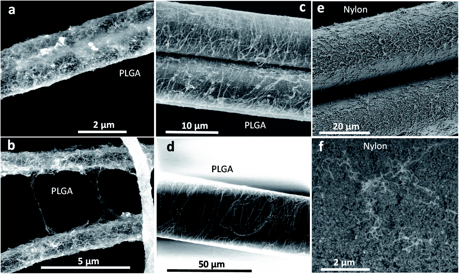 | ||
| Fig. 1 SEM images of silver NW coated PLGA and nylon fibres: (a and b) thin PLGA fibres (∼1–2 μm in diameter) coated with NWs, (c) Thicker PLGA fibres (∼10 μm) and (d) (∼40 μm) coated with NWs. (e) SEM image of the 25 μm nylon 6:6 fibres coated with NWs. (f) A higher magnification image of the surface of a NW-coated nylon fibre. Note that only the thicker NWs are visible here and there are probably invisible thinner ones covering the surface. | ||
The different NW arrangements on PLGA fibres of different diameters could be explained by considering the persistence length of the CTAB surfactant self-assembled nanostructures, which probably forms an elongated tubular template for the formation of the NWs. For worm-like micelles, the persistence length is defined as the length over which the micelles are considered rigid.25 For charged wormlike micelles (as in CTAB), the persistence length varies significantly with the surfactant structure, counter-ion, and salt concentration. For CTAB, persistence lengths that vary from tens of nm to ∼1 μm were reported, depending on the specific conditions of the measured system.26–30 Here we assume that the tubular CTAB template (including complexed metal ions), which is rolled around the seed particles and supports the growth of the NWs, has a persistence length in the order of 1 μm. This magnitude of persistence length would prevent the NWs from coiling around the thin (∼1–2 μm) fibres but will allow them to wrap around the ∼10–40 μm thick fibres. This concept is further supported by the observation that in the case of the 40 μm PLGA fibres, the transverse organization of the NWs is significantly more pronounced relative to the 10 μm fibres.
In the case of the nylon fibres, the formed NW network was more granular and rough, without wrapping around the fibres, as can be seen in Fig. 1e and f. This indicates the different organization of CTAB on the nylon surface and probably a different NW growth scheme. We believe that the reason for the NWs not coiling around the 25 μm nylon fibres should be related to the mode of assembly of the CTAB nanostructures at the polymer surface. While PLGA is hydrophobic, nylon is more hydrophilic, and consequently, the interaction of CTAB with the surface is expected to differ significantly.31 The surface roughness was also observed to affect the assembly of CTAB.32 It should be stressed that in general, growing the NW network on the nylon fibres was more difficult than growing them on PLGA and required more careful tuning of surface preparation by plasma treatment of the nylon fibres and the obtained sheet resistance (to be discussed below) was higher compared to the coated PLGA fibres.
To measure the electrical resistance of the NW decorated fibres, single fibres were glued at two points along the fibre to an insulating surface using silver paint, which acted also as electrical contacts, and the resistance of the fibre was measured (Fig. 2). Measurements performed on several single PLGA fibres with a diameter of 10–40 μm and ∼1 cm in length indicated a sheet resistance of 30 ± 5 Ω sq−1, calculated from the dimensions of the coated fibres. Similar sheet resistance values were obtained for the NW-coated nylon fibres after much thicker silver coating, which apparently reduced the coating transparency.
 | ||
| Fig. 2 Resistance measurement of a single PLGA fibre of 20 μm in diameter and ∼1 cm in length. The 5.18 kΩ resistance is translated to a sheet resistance of 32 Ω sq−1 using the dimensions of the fibre. The inset shows a zoom-in view of the silver-paint contacted fibre. | ||
The NW coating is not limited to single fibres and can be utilized on fabrics. Fig. 3 presents the growth of silver NWs on nonwoven meshes of thin PLGA fibres with fibre diameters in the range of 2–5 μm. As was demonstrated above, the growth of NWs on single fibres with a diameter of 2 μm did not exhibit a preferential growth direction. In the dense fabric, however, the proximity of the fibres resulted in the growth of NWs around multiple adjacent fibres, with an effective bundle diameter of ∼10 μm. Under these conditions, the NWs again exhibited directional growth transverse to the main axis of the adjacent fibres, coiling around the bundle similar to the behavior exhibited on thick fibres. The continuous growth of the NWs around the bundles was achieved also in the cases where there were small gaps between the fibres, indicating the relatively weak interaction of the CTAB template with the fibre surface and the importance of the properties of the CTAB template itself, supporting the role of the persistence length in determining the organization of the NWs around the fibres.
 | ||
| Fig. 3 (a–d) SEM images of the silver NW coated PLGA fabric-like substrate formed of thin fibres (1–2 μm). Inset: an image of the silver NW coated PLGA fabric-like substrate glued to a PET frame. | ||
In addition, bundles of NWs with lengths of tens of micrometres were observed to extend between distant fibres, indicating that the NWs grow out of the fibres' surfaces. This may occur either because the CTAB template forms a continuous film between adjacent fibres or due to partial detachment of weakly bound NWs from the fibre surface. Then the floating NWs could continue to grow in the solution until eventually reaching and attaching to a distant fibre.
A key requisite for utilizing the methodology for producing flexible and stretchable electronics is the ability of the NW-coated fibres and fabrics to maintain their conductance while being significantly stretched or deformed. To examine the effect of pulling on the electrical resistance at the single-fibre level, we used NW-coated commercial nylon 6:6 fibres. In a typical experiment, the NW coated nylon fibre was glued over a PET frame at both edges using silver paint fortified by epoxy glue coating. The silver paint acted as a contact point for the measurement of the resistance (Fig. 4a). The frame was clamped onto a manually operated load device, and then it was cut at both sides to allow free pulling of the fibre only. The resistance was measured while stretching the fibre by turning the micrometer screw until a strain of ∼10–15% was reached. Then, in some of the experiments, the fibre was allowed to relax back to its original length.
 | ||
| Fig. 4 (a) A schematic illustration of the fibre-stretching device together with the loaded PET frame, holding the single nylon fibre coated with the conductive NW mesh, with glued electrical contacts. (b) Resistance vs. elongation for repeated stretch-and-release experiments, demonstrating an initial increase of resistance on the first stretch, and nearly constant resistance during the next cycles, ending with a steep increase in resistance due to breaking of the NW network at elongation above 10%. | ||
Fig. 4b shows a typical resistance vs. elongation curve measured during four stretch-and-release cycles. In the first stretch cycle, a significant four-fold increase in the resistance occurred. We believe that this initial resistance increase is due to breaking of weak contacts either in the silver paint at the electrical contacts to the coating, or within the NW coating itself. We were not able to obtain evidence for structural changes in the NW network, which may have occurred on stretching. However, SEM imaging of the contact area of the nylon fibres did show that the pulling resulted in partial breaking of the contact (see ESI, Fig. S2†). Qualitatively similar behaviours were observed in stretching experiments of several coated nylon fibres (see ESI, Fig. S3†).
In the following stretching and relaxation cycles (Fig. 4b), there was an additional gradual loss of conductance, down to ∼0 at 12–15% strain, where a large resistance jump occurred, probably due to the breaking of the NW network, which in the case of the NW coated nylon fibres seems to possess a relatively stiff morphology. Interestingly, in each relaxation step, part of the conductance was restored, perhaps due to the re-establishment of some of the physical (and consequent electrical) contacts in the broken NWs. This picture is consistent with the observation of resilience of such NW films deposited on PET substrates in bending tests (ref. 24, ESI).
The potential use of such a system as a strain sensor was examined by looking at the gauge factor.36 Plotting the logarithm of the normalized resistance vs. strain for the first stretch in Fig. 4b roughly shows an exponential strain gauge behaviour (see ESI, Fig. S4†). The slope was Gexp ∼ 4.8, which is in the range of the gauge factors of continuous thin metal foils. Silver or gold nanoparticle based conductive thin films should have much higher gauge factor values.37 The nearly bulk metal film value of Gexp can be attributed to the weak interaction of the NW network with the nylon fibre and to the robustness of the NW network. Upon applying stress to the fibre, part of the NW network can probably slide over the substrate at weak adhesion points and the network morphology can change to accommodate the stress. Thus, effectively, part of the NW film may experience lower stress than applied to the fibre.
It should be noted that similar stretching experiments could not be performed with individual PLGA fibres because they exhibit a significantly lower yield strength compared with nylon and easily tear down at a low strain.
Stretch and release experiments were also performed on a NW-coated nonwoven mesh of PLGA fibres (fibre diameter ∼ 800 nm). Unlike the case of a single PLGA fibre, the meshes exhibit significant robustness to stretching. Similar to the single nylon fibres, a significant increase in resistance was observed throughout the first stretching cycle (Fig. 5), which we again attribute to the breaking of weak contacts in the NW network, or in the silver paint contact area. In the subsequent repeated stretch and relaxation cycles, the resistance remained almost constant with small reversible changes during each cycle, as long as the elongation remains below 25%. This is probably due to the difference in the way a fabric is stretched relative to a single fibre; in the single fibres, the whole elastic strain occurs in the individual polymeric fibre, while in the fabric, the stress is translated mainly to a morphological change in the mesh. Notably, a significant strain at the fibre level occurs only once the fabric mesh is fully stretched, i.e. all the fibres become aligned with the stretch direction. Hence, in the present case, there seems to be only a slight breaking of the NW network as long as the elongation is <25%.
 | ||
| Fig. 5 Resistance vs. elongation curves measured by stretching and relaxing a thin PLGA fibre fabric coated with the NW film. Again, the first stretch might result in breaking of weak contacts in the NW network or in the silver paint contact area already at a few % elongation, followed by a sharp increase in resistance as the elongation reaches ∼25%. | ||
The NW coating of the fibres is ultra-thin (tens of nm thickness) and fairly transparent. Despite this low amount of metal mesh coating, both the single fibres and non-woven fabrics exhibit significant conductance and stretch resilience of conductivity. Other groups have mainly studied relatively thick fibres of composites of polymers and silver NWs for flexible electronics.18,33–35 In the cases of high metal loading, they could maintain electrical conductivity even with 100% strain. In our case, more modest results are achieved with orders of magnitude lower metal concentration and much thinner fibres. Our typical metal loading values are about 3–6 ng (for ∼5–10% area coverage) silver (being the main metal in the coating) per 1 cm length of a 10 μm diameter fibre. The metal loading could be changed over a wider range by changing the silver deposition duration in the last coating step.38
4. Conclusions
We have presented a new approach for producing conductive flexible polymeric fibres and fabrics of different diameters and materials by the growth of a gold–silver NW conductive layer directly on their surface. The plasticity of the metallic NW network enables the retention of the conductivity under strain, with single fibres exhibiting conductance up to a strain level in the range of 8–20% and fabrics exhibiting significant conductance up to a higher elongation level of ∼25%. The morphology of the NW network depends on the polymer properties; however, as demonstrated for PLGA fibres it is also affected by the fibre diameter, shifting from a disordered mesh for fibres <5 μm diameter, to a highly oriented, transverse wrapping at ≥10 μm diameter fibres. The approach described here is highly flexible and general and can be utilized for forming a conductive and transparent layer on different polymeric fibres (with an appropriate surface treatment, if needed), both at the single-fibre level and on preformed fabric. Hence, it offers a scalable and generic method for the large-scale production of electronic fabrics with minimal amounts of metal coating for a range of applications.Conflicts of interest
There are no conflicts to declare.Acknowledgements
This work was supported in part by the Tel Aviv University's Ramot Momentum Fund (GM), and in part by the RDECOM-Atlantic, and US Army Research Office under Grant Number W911NF-18-1-0321 (AS). The views and conclusions contained in this document are those of the authors and should not be interpreted as representing the official policies, either expressed or implied, of the U.S. Government. The U.S. Government is authorized to reproduce and distribute reprints for government purposes notwithstanding any copyright notation herein. A. Sitt acknowledges the generous support from the Azrieli Foundation. S. Ziv Sharabani acknowledges the generous support of The Shulamit Aloni Scholarship for Advancing Women in Exact Science and Engineering, provided by The Ministry of Science & Technology, Israel.References
- Y. Wu, S. S. Mechael and T. B. Carmichael, Acc. Chem. Res., 2021, 54, 4051–4064 CrossRef CAS PubMed.
- M. Zhang, K. R. Atkinson and R. H. Baughman, Science, 2004, 306, 1358–1361 CrossRef CAS PubMed.
- L. Hu, M. Pasta, F. La Mantia, L. F. Cui, S. Jeong, H. D. Deshazer, J. W. Choi, S. M. Han and Y. Cui, Nano Lett., 2010, 10, 708–714 CrossRef CAS PubMed.
- J. Wu, D. Zhou, C. O. Too and G. G. Wallace, Synth. Met., 2005, 155, 698–701 CrossRef CAS.
- J. Molina, A. I. del Río, J. Bonastre and F. Cases, Eur. Polym. J., 2008, 44, 2087–2098 CrossRef CAS.
- A. Varesano and C. Tonin, Text. Res. J., 2008, 78, 1110–1115 CrossRef CAS.
- K. H. Hong, K. W. Oh and T. J. Kang, J. Appl. Polym. Sci., 2005, 97, 1326–1332 CrossRef CAS.
- S. Takamatsu, T. Lonjaret, E. Ismailova, A. Masuda, T. Itoh and G. G. Malliaras, Adv. Mater., 2016, 28, 4485–4488 CrossRef CAS PubMed.
- D. Knittel and E. Schollmeyer, Synth. Met., 2009, 159, 1433–1437 CrossRef CAS.
- H. Kim and J. H. Ahn, Carbon, 2017, 120, 244–257 CrossRef CAS.
- C. Wu, T. W. Kim, F. Li and T. Guo, ACS Nano, 2016, 10, 6449–6457 CrossRef CAS PubMed.
- C. Wu, T. W. Kim, T. Guo and F. Li, Nano Energy, 2017, 32, 367–373 CrossRef CAS.
- Z. H. Lim, Z. X. Chia, M. Kevin, A. S. W. Wong and G. W. Ho, Sens. Actuators, B, 2010, 151, 121–126 CrossRef CAS.
- T. Lee, W. Lee, S. W. Kim, J. J. Kim and B. S. Kim, Adv. Funct. Mater., 2016, 26, 6206–6214 CrossRef CAS.
- M. Zhukovskyi, L. Sanchez-Botero, M. P. McDonald, J. Hinestroza and M. Kuno, ACS Appl. Mater. Interfaces, 2014, 6, 2262–2269 CrossRef CAS PubMed.
- P. C. Hsu, X. Liu, C. Liu, X. Xie, H. R. Lee, A. J. Welch, T. Zhao and Y. Cui, Nano Lett., 2015, 15, 365–371 CrossRef CAS PubMed.
- D. Doganay, S. Coskun, S. P. Genlik and H. E. Unalan, Nanotechnology, 2016, 27, 435201 CrossRef PubMed.
- S. Lee, S. Shin, S. Lee, J. Seo, J. Lee, S. Son, H. J. Cho, H. Algadi, S. Al-Sayari, D. E. Kim and T. Lee, Adv. Funct. Mater., 2015, 25, 3114–3121 CrossRef CAS.
- Y. Cheng, R. Wang, J. Sun and L. Gao, ACS Nano, 2015, 9, 3887–3895 CrossRef CAS PubMed.
- H. W. Cui, K. Suganuma and H. Uchida, Nano Res., 2015, 8, 1604–1614 CrossRef CAS.
- Y. Atwa, N. Maheshwari and I. A. Goldthorpe, J. Mater. Chem. C, 2015, 3, 3908–3912 RSC.
- T. E. Glier, M. Betker, M. Witte, T. Matsuyama, L. Westphal, B. Grimm-Lebsanft, F. Biebl, L. O. Akinsinde, F. Fischer and M. Rübhausen, Nanoscale, 2020, 12, 23831–23837 RSC.
- D. Azulai, E. Cohen and G. Markovich, Nano Lett., 2012, 12, 5552–5558 CrossRef CAS PubMed.
- M. E. Layani-Tzadka, E. Tirosh and G. Markovich, ACS Omega, 2017, 2, 7584–7592 CrossRef CAS PubMed.
- C. A. Dreiss, Soft Matter, 2007, 3, 956–970 RSC.
- T. Imae and S. Ikeda, J. Phys. Chem., 1986, 90, 5216–5223 CrossRef CAS.
- W. J. Kim and S. M. Yang, Adv. Mater., 2001, 13, 1191–1195 CrossRef CAS.
- D. Grabner, L. Zhai, Y. Talmon, J. Schmidt, N. Freiberger, O. Glatter, B. Herzog and H. Hoffmann, J. Phys. Chem. B, 2008, 112, 2901–2908 CrossRef CAS PubMed.
- M. E. Helgeson, T. K. Hodgdon, E. W. Kaler and N. J. Wagner, J. Colloid Interface Sci., 2010, 349, 1–12 CrossRef CAS PubMed.
- W. Zou, X. Tang, M. Weaver, P. Koenig and R. G. Larson, J. Rheol., 2015, 59, 903 CrossRef CAS.
- J. F. Liu and W. A. Ducker, Langmuir, 1999, 103, 8558–8567 CAS.
- S. Wu, L. Shi, L. B. Garfield, R. F. Tabor, A. Striolo and B. P. Grady, Langmuir, 2011, 27, 6091–6098 CrossRef CAS PubMed.
- C. Lu, S. Park, T. J. Richner, A. Derry, I. Brown, C. Hou, S. Rao, J. Kang, C. T. Moritz, Y. Fink and P. Anikeeva, Sci. Adv., 2017, 3, e1600955 CrossRef PubMed.
- Y. Lu, J. Jiang, S. Yoon, K. S. Kim, J. H. Kim, S. Park, S. H. Kim and L. Piao, ACS Appl. Mater. Interfaces, 2018, 10, 2093–2104 CrossRef CAS PubMed.
- G. J. Zhu, P. G. Ren, H. Guo, Y. L. Jin, D. X. Yan and Z. M. Li, ACS Appl. Mater. Interfaces, 2019, 11, 23649–23658 CrossRef CAS PubMed.
- M. A. O'Mara, S. P. Ogilvie, M. J. Large, A. Amorim Graf, A. C. Sehnal, P. J. Lynch, J. P. Salvage, I. Jurewicz, A. A. K. King and A. B. Dalton, Adv. Funct. Mater., 2020, 30, 2002433 CrossRef.
- M. Segev-Bar and H. Haick, ACS Nano, 2013, 7, 8366–8378 CrossRef CAS PubMed.
- M. E. Layani-Tzadka, D. Krotkov, E. Tirosh, G. Markovich and S. Fleischer, Nanotechnology, 2019, 30, 215702 CrossRef CAS PubMed.
Footnotes |
| † Electronic supplementary information (ESI) available. See DOI: 10.1039/d1na00872b |
| ‡ These authors contributed equally to this work. |
| This journal is © The Royal Society of Chemistry 2022 |