
Air-gap embedded triboelectric nanogenerator via surface modification of non-contact layer using sandpapers†
Inkyum
Kim
,
Hyeonhee
Roh
,
Wontae
Choi
and
Daewon
Kim
 *
*
Department of Electronic Engineering, Institute for Wearable Convergence Electronics, Kyung Hee University, 1732 Deogyeong-daero, Giheung-gu, Yongin 17104, Republic of Korea. E-mail: daewon@khu.ac.kr
First published on 30th April 2021
Abstract
With the increased number of small electronics and demand for their energy source, renewable energy sources have received much attention. Above all, a triboelectric nanogenerator (TENG) based on the combination of contact electrification and electrostatic induction has been researched as a method of converting mechanical energy into electricity. In order to increase the electrical output of TENGs with raising the surface charge density, a lot of researchers have focused on the fabrication methods to employ micro-/nano-structures onto a contact surface of the TENG, but have been facing several issues regarding the degradation of the output performance from the iterative operation process. Hence, it is highly required to introduce an approach to enhancing the performance of TENG, while minimally degrading the output power during the long-term operation. In this paper, an air-gap embedded TENG (AE-TENG), which contains a microstructure on the non-contact surface by means of a sandpaper, is proposed. These small air-gaps between the spin-coated polydimethylsiloxane and the non-contact surface can significantly boost the total surface charge density of the dielectric layer. Thus, the electrical output performance of the AE-TENG is enhanced without any surface engineering on the contact surface. Furthermore, the effect of the air-gap induced surface charges on the electric potential is systematically analyzed by not only experimentally electrical outputs, but theoretical and computational modeling based on the V–Q–x relationship and simulation software tool. This air-gap induced triboelectric effect opens a new perspective of the development of electrical outputs by providing a structural/theoretical understanding for TENGs.
1. Introduction
Nowadays, the rapid development of the information technology and internet of things highly requires a reusable and sustainable power source to drive plenty of small electronics around us. Energy harvesting devices that can convert the various types of renewable and green energy sources into an electrical energy using piezoelectric, photovoltaic, thermoelectric, electromagnetic, and triboelectric effects are great alternatives for the conventional power sources.1–5The triboelectric nanogenerator (TENG) based on the coupling of contact electrification and electrostatic induction has been attracting tremendous interest among the aforementioned energy harvesting devices due to the merits of high power density and conversion efficiency in converting mechanical energy into electricity.6–10 The four operation types of TENGs with vertical contact-separation mode, contact-sliding mode, single electrode mode, and freestanding triboelectric-layer mode allow for the use of any kind of mechanical movements, such as contact-separation, rotation, sliding, and impact as input sources.11–19 This wide applicability of TENGs allows the fabricated energy harvesting device to expand the application for self-powered sensor systems, self-powered charging systems, and secondary power sources.20–26 Moreover, it has been proven that TENGs have advantages in its wide spectrum of material selection, facile fabrication process, and eco-friendly characteristic.
Previous studies have dealt with improving the electrical output performance of TENGs in order to strengthen its role as a power source, one of the main applications of TENGs. A variety of approaches, such as an injection of charges onto the contact surface, a modulation of dielectric constant of the contact materials, selection of the materials showing the large difference of electron affinity, and hybridization with other energy harvesting technology, were adopted to enhance the output performance of TENGs.27–38 Among these various approaches, one of the primitive and simple methods of improving the electrical power of TENGs is the enlargement of an effective contact surface area using a micro-/nano-structure employed on the contact surface, which increases the surface charge density induced by the contact electrification.14,39–51 However, this micro-/nano-structure on the contact layer is inevitably destroyed and damaged during the basic contact-separation process of TENGs, which leads to a remarkable degradation of the output performance during the long-term operation. Thus, it is greatly required to select an approach for enhancing the performance of TENGs without degradation of the output power during long-term operation using simple and cost-effective methods.
In this study, the performance of the contact-separation mode TENGs is enhanced by embedding an air-gap at a non-contact surface of a bottom layer. The Al-coated microstructure on the non-contact surface is formed by polishing a polyimide (PI) film with commercial sandpapers with various grit numbers and depositing a metal layer. After the pre-fabricated layer is covered with a spin-coating process of the polydimethylsiloxane (PDMS), the air-gap can be naturally formed between the coated dielectric (PDMS) and electrode layers. Two steps of experiments are designed to systematically evaluate the effect of this air-gap on the electrical output. First, the effect of the grit number of the sandpapers on the air-gap distance is investigated. The optimized air-gap distance is discovered by measuring the electrical outputs with changing the grit number of the sandpaper. Based on this optimization, the electrical outputs of the air-gap embedded TENG (AE-TENG) are compared to that of other TENGs of normal TENG, structured (contact surface-modified) TENG, and structured AE-TENG (combined structure of the structured TENG and AE-TENG) to verify the improved surface charge density and existence of an additional electric field. The role of the air-gap in the non-contact layer can be proved with theoretical formula results using the mathematical modeling and calculation of the electric potential distribution by a simulation software. Through this cost-effective, less time-consuming, and easy fabrication process using sandpapers, the structured AE-TENG can generate electricity with great durability even after innumerable contact-separation process with establishing the theoretical perspective for enhancing the electrical output of TENG.
2. Experimental
2.1. Fabrication of TENG using a sandpaper
The well-known contact-separation mode TENG composed of two electrodes and a dielectric layer was adopted for establishing the basic structure. In this study, four kinds of the contact-separation TENG were prepared: normal TENG, structured TENG, AE-TENG, and structured AE-TENG. At the top part of the sandpaper polishing-case, the polyimide (PI) film with the dimension of 4.5 × 5 cm2 and thickness of 125 μm served as a substrate layer. To fabricate the uniform microstructures on the contact and non-contact surfaces, the PI film was polished by a sandpaper with the 1200# grit number, and this polishing process was achieved with the aid of the lab-made equipment for the equivalent sanding condition. After that, the remaining particles attached to the surface of the PI film were completely removed by ultrasonication process. The electrode layer, which is composed of Cr (40 nm) and Al (200 nm) deposited layers, was deposited on the PI film by using a thermal evaporation system. Al was adopted as a main electrode material due to the easy availability with the form of a foil or a tape compared to other metals. With using the adhesion metal layer of Cr, the electrode layer on the substrate showed high physical stability through a detaching test employing a commercial transparent tape. After the tape attaching and detaching test with the Cr/Al deposited surface, the resistance remained at a small value of 2.6 Ω, as shown in Video S1.† As another substrate, a polytetrafluoroethylene (PTFE) film with the thickness of 100 μm was used to fabricate the four types of TENGs. The same fabrication process with the PI substrate-case was conducted to fabricate the samples with the PTFE substrate.Polydimethylsiloxane (PDMS) (Sylgard 184, Dow Corning) was selected as the contact dielectric layer that was developed on the corrugated surface of the bottom electrode because of the high flexibility and compatibility of the PDMS. First, a PDMS solution was prepared with mixing the base elastomer and the curing agent at a mass ratio 10![[thin space (1/6-em)]](https://www.rsc.org/images/entities/char_2009.gif) :1. Then, the solution was poured on the electrode and subsequently spin-coated at 500 rpm for 10 seconds. The PDMS-coated layer was thermally cured in the convection oven at 150 °C for 10 minutes.
:1. Then, the solution was poured on the electrode and subsequently spin-coated at 500 rpm for 10 seconds. The PDMS-coated layer was thermally cured in the convection oven at 150 °C for 10 minutes.
2.2. Measurement and characterization
The mechanical input force to operate the TENGs was applied by an electrodynamic shaker (Labworks Inc. ET-139) connected to a function generator (Keysight 33120A). The function generator created a square wave signal with varying frequency and amplitude. The basic electrical outputs, such as the open-circuit voltage (VOC) and short-circuit current (ISC), were measured by using a system electrometer (Keithley Model 6514). The microstructure on the polished surfaces, which was formed by sandpapers, was investigated using a field emission scanning electron microscope (FE-SEM, Carl Zeiss MERLIN).3. Results and discussion
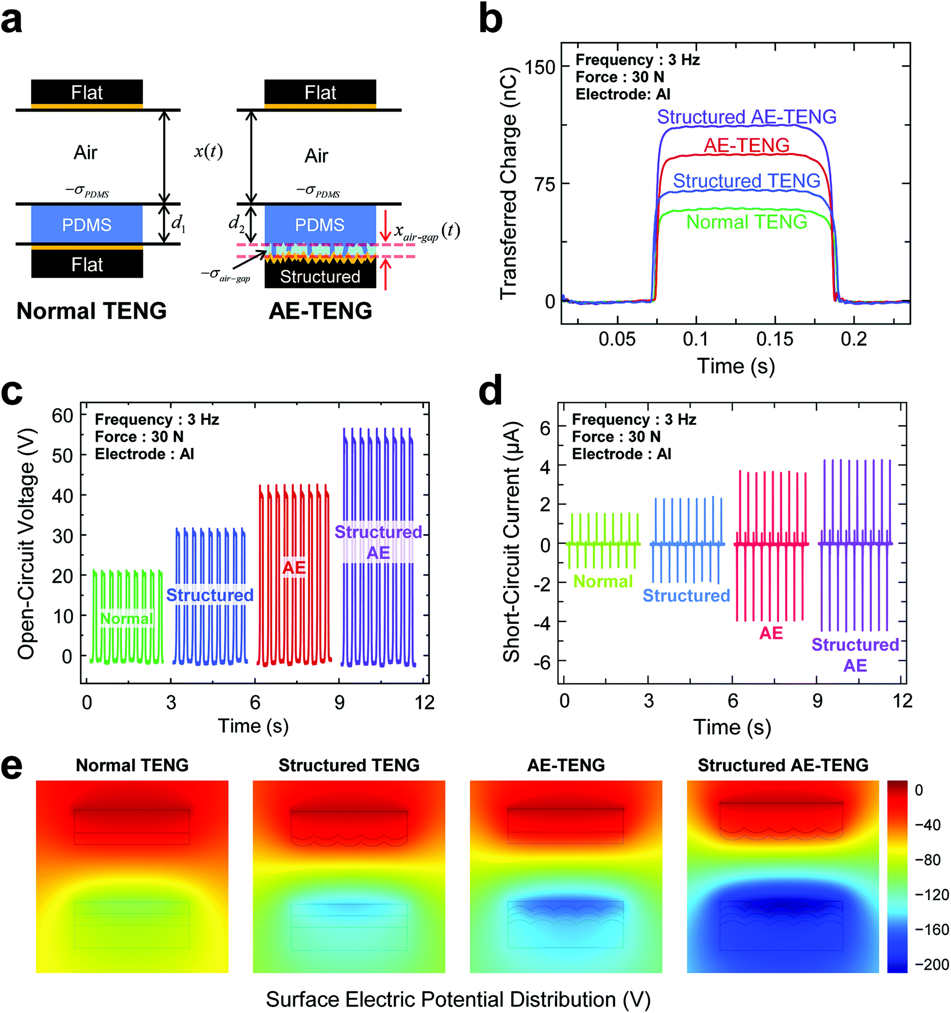
Fig. 1a depicts a structured air-gap embedded triboelectric nanogenerator (AE-TENG) with the direct sandpaper-case composed of top and bottom layers. The structured layer was derived from the microstructure of a commercially available sandpaper. The electrode was directly formed on the surface of the sandpaper by thermal deposition of the metal layer. The only difference of the composition between the top and bottom layers is the existence of the polydimethylsiloxane (PDMS) layer on the electrode layer. Fig. 1b shows the scanning electron microscope (SEM) image of the surface of the sandpaper with a 1200# grit number. Also, the surfaces of sandpapers with other grit numbers ranging from 60# to 20000# were confirmed by using SEM, as shown in Fig. S1.† The commercial sandpaper with the higher grit number represented a smaller average diameter of particle. The average particle size of the sandpaper decreased, ranging from 300 μm to 0.4 μm, as the grit number increased, ranging from 60# to 20000#, as shown in Fig. S2.†
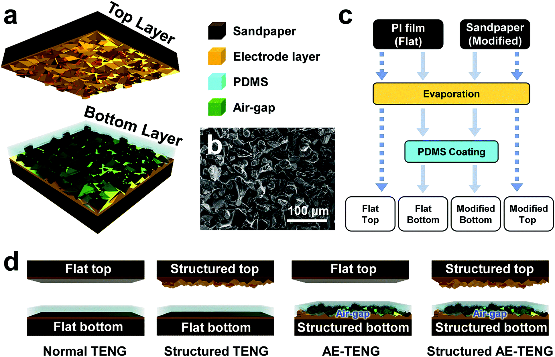 | ||
| Fig. 1 (a) Schematic illustration of the structured air-gap embedded (AE) TENG. (b) SEM image of the sandpaper (1200#) showing the micro-structured surface. (c) Schematic diagram of the fabrication process, and (d) cross-section of the four types (normal TENG, structured TENG, AE-TENG, and structured AE-TENG) of TENGs. | ||
To investigate the influence of the inherent microstructure of the sandpaper on the electrical characteristic of the TENG, four kinds of TENGs with the combination of two types of top layers and another two types of bottom layers were prepared, as shown in Fig. 1c. The flat layer was composed of the Al deposited polyimide (PI) film substrate, whereas the structured layer was fabricated by using the Al deposited sandpaper substrates. Additionally, the PDMS layer was coated only on the bottom layer by using a spin-coater to function as a dielectric layer. Consequently, the four types of TENGs, i.e., the normal TENG (normal), structured TENG (top side, TS), AE-TENG (bottom side, BS), and structured AE-TENG (double side, DS), were constructed by pairing each fabricated layer shown in Fig. 1d. In the case of the normal TENG, which consisted of a flat top layer and flat bottom layer, there was no microstructure on both layers. On the other hand, the structured TENG and AE-TENG have microstructures rising from the sandpaper on the top and bottom surface layers, respectively. The structured TENG is one of the representative models, which has been studied in previous papers, to increase the effective contact surface area by employing the micro-/nano-structure, which leads to an improvement of the electrical output from the TENGs.14 However, unlike the structured TENG, the AE-TENG contains microstructures on the non-contact surface layers, i.e., bottom electrodes. The inherently formed air-gap layer between the bottom electrode and PDMS can serve as a dielectric layer. These air-gaps were formed due to the low surface energy in the non-contact electrode compared to that in the PDMS layer.52 Lastly, the structured AE-TENG was composed of a combined structure with the top and bottom layers from the structured TENG and AE-TENG, respectively. Hence, this structured AE-TENG contained the microstructure on both contact and non-contact electrode surfaces.
Fig. 2a and b shows the measured electrical outputs under three different levels of the input force applied to the four types of TENGs. Four TENGs were operated in the contact-separation mode with the weak, middle, and strong force, which corresponds to 5, 10, and 30 N, respectively. These inputs were vertically applied by using an electrodynamic shaker under the same frequency of 3 Hz. With the amplitude of the input force, the partial or complete contact at the contact surface can be determined. When applying the lowest input force of 5 N to each TENG, the open-circuit voltage (VOC) and short-circuit current (ISC) of the AE-TENG showed the highest values, followed by those of the structured AE-TENG, normal TENG, and structured TENG in order. With this lowest input force, the air-gap of the non-contact surface was repeatedly pressed, whereas the partial contact occurred at the contact surface. It is noteworthy that the AE-TENG and structured AE-TENG, which both inherently contain the air-gap between the dielectric layer and electrode layer, showed higher electrical outputs than the normal TENG and structured TENG without the air-gap. In addition, the incomplete contact at the contact surface of the structured TENG reduced the effective contact area, and lower electrical outputs were produced compared to that of the normal TENG. By the same reason, the electrical outputs of the structured AE-TENG were lower than those of the AE-TENG.
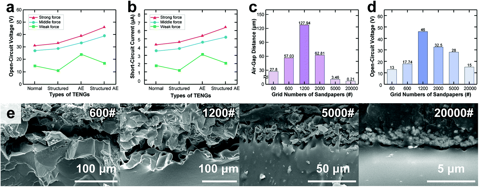 | ||
| Fig. 2 (a) The open-circuit voltage (VOC) and (b) short-circuit current (ISC) of the four types of TENGs. (c) The measured thickness of the air-gap and (d) VOC with various grit numbers of commercial sandpapers. (e) The scanning electron microscope (SEM) images for the cross-section showing an air-gap between the dielectric layer and metal layer with various grit numbers of commercial sandpapers ranging from 600#, 1200#, 5000#, and 20000#. | ||
After increasing the applied force, as shown in Fig. 2a and b, the order of the electrical outputs with different TENGs was changed. The structured AE-TENG represented the highest electrical outputs, followed by the AE-TENG, structured TENG, and normal TENG in descending order. As the applied force was increased, the complete contact-separation process was induced at the contact surface located between the structured top layer and PDMS layer. Therefore, the structured TENG generated higher outputs than the normal TENG, and the structured AE-TENG also produced higher outputs than the AE-TENG.
As shown in Fig. 2c, the air-gap distance in the non-contact layer was checked with different grit numbers of the sandpapers. The thinner air-gap is caused by the stronger adhesion between the PDMS and Al-coated sandpaper layers, and this bonding is stronger with enlarging flat surface area of the sandpapers. For example, the sandpaper with the higher grit number composed of the smaller size of the particle and mainly consisted of the flat surface can easily maintain the bonding state with the PDMS layer. Therefore, the air-gap distance with the 20000# grit number sandpaper was significantly reduced compared to that of the 1200# grit number sandpaper. However, even at lower grit number sandpaper, there was a limitation in increasing the air-gap distance due to the lower distribution density of the particles. As shown in Fig. S1,† as the grit number of the sandpaper decreased, the density of the particles also decreased with significantly extending the flat surface area of the sandpaper. As a result, with a similar mechanism to the formation of the air-gap at the high grit number sandpaper, the adhesive area between the sandpaper and PDMS layer was widened, leading to a decrease in the air-gap distance. In other words, the sandpaper with high grit number can be considered as a flat surface and the air-gap distance was decreased. Therefore, from these two results, an optimum point of forming the highest air-gap distance was found in the 1200# sandpaper.
The existence of the air-gap between the PDMS layer and micro-structured electrode layer can be confirmed by the cross-sectional SEM images of each bottom layer with different grit numbers of sandpapers, as shown in Fig. 2e. Additionally, the air-gap distances and measured open-circuit voltages with various grit numbers of sandpapers were verified in Fig. 2c and d, respectively. The AE-TENG with the higher air-gap distance can generate the larger open-circuit voltage by matching these two measured results. Then, it can be considered that the higher air-gap distance could enhance the accumulated triboelectric charges underneath the PDMS layer, resulting in higher electric potential difference between the top and bottom electrodes. Compared with the output voltage values of the 600# and 2000# cases, the higher output voltage was measured in the 2000# case, even though the air-gap distance is similar. This result appeared with the larger full contact area using the 2000# sandpaper due to the smaller particle size compared to the 600# sandpaper.
As shown in Fig. 2, the enhanced electrical output of the AE-TENG is attributed to the existence of the air-gap formed between the PDMS and Al-coated sandpaper. However, the random structures of the sandpapers formed by different sizes of particles can disturb the quantitative analysis. A uniform and more physically stable artificial structure needs to be formed as a structured layer. Accordingly, as shown in Fig. 3a, a sandpaper polishing-case was adopted to conduct a reliable quantitative analysis. A PI film was adopted as a polymer-based substrate layer, which is able to be scratched by the sandpaper, but shows a flat and rigid characteristic. This PI film was polished with the 1200# sandpaper to create the uniformly structured layer. A lab-made equipment was used to rotate the sandpaper layer at a high speed, and the PI film was placed on the sandpaper layer with the application of a constant pressure for the homogeneous polishing. After this polishing process, the structured PI film was ultrasonicated to remove the residues caused by the sandpaper, and the 40 nm of Cr and 200 nm of Al layers were deposited on the PI film by using the thermal evaporation system. For fabricating the dielectric layer for the TENG, a PDMS layer was also coated. The optical image and the surface and cross-sectional SEM images of the fabricated flat and structured layers are shown in Fig. 3b–d. On the surface of the structured layer, the scratched lines can be discovered, while no surface structure was observed for the flat layer in the optical image and top view SEM images. The width of the scratched lines created on the PI film was maintained at nearly 50 μm, since the average size of particle of the 1200# sandpaper is 50 μm, as represented in Fig. S2.† The air-gap existing in the structured layer is shown in the cross-sectional side view in Fig. 3d, which is contrary to that of the flat sample shown in Fig. 3c.
 | ||
| Fig. 3 (a) Illustrated schematics of the fabrication process for the structured layer by using chemical mechanical polishing. (b) Digital photographs of the Al-coated flat and structured layer. The SEM images of the top-view and cross-section of (c) the flat layer and (d) structured layer. | ||
Generally, the fundamental mechanism of the TENG for generating electrical energy is based on the conjunction of the triboelectric effect, and electrostatic induction from the contact-separation process between the top and bottom layers. Because of the different triboelectric properties of the top Al layer and bottom PDMS layer, the triboelectric charge and potential difference are induced at the contact surfaces and two electrodes, respectively during the contact-separation motion.
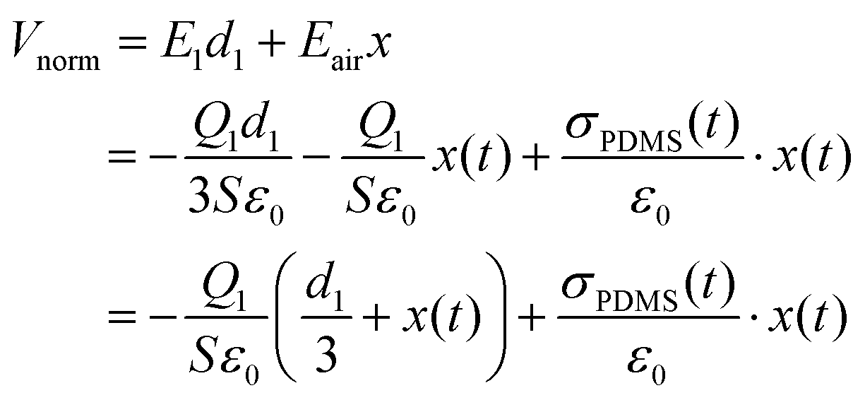
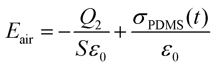
Fig. 4a shows the schematic models to demonstrate a theoretical study for the normal and the AE-TENG. The simplified V–Q–x relationship for the contact-mode TENGs was adopted in this study; V is the potential difference between the two electrodes, Q is the amount of the transferred charge, and x is the separation distance between the two triboelectric charged layers.53–55 Assuming that the electrons on the metal are uniformly delocalized over the metal surface, the electric fields at the dielectric layer and the air derived by Poisson's equation are as follows:
Inside the dielectric:
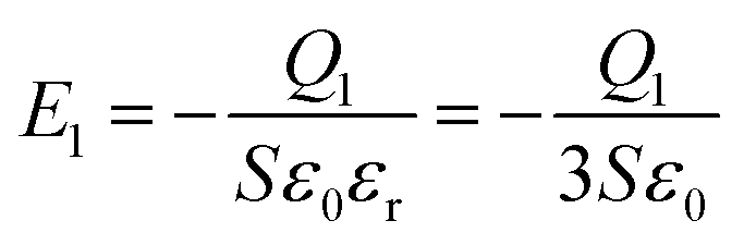 | (1) |
Inside the air:
 | (2) |
Here, S is the area of the metal layers, and the relative permittivity of the PDMS is 3. Based on the simplified V–Q–x relationship, Vnorm can be derived as the following equation.
 | (3) |
 | ||
| Fig. 4 (a) Schematic diagram describing the theoretical modeling for normal TENG and AE-TENG. (b) The amount of transferred charges (Qtr), (c) open-circuit voltage (VOC), and (d) short-circuit current (ISC) of the four types of TENGs at a vibration frequency of 3 Hz and an applied force of 30 N. (e) The visualization of the electric potential distribution of the four types of TENGs simulated by using a simulation software. | ||
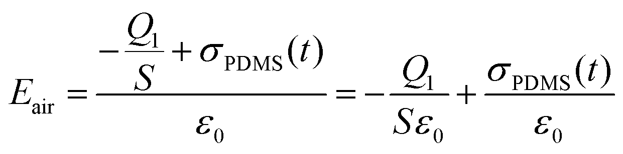
However, in the case of the AE-TENG, a parameter for the air-gap layer should be considered. Hence, an equation related to the additional electric field is added in the following equations.
Inside the dielectric:
 | (4) |
Inside the air:
 | (5) |
Inside the air-gap:
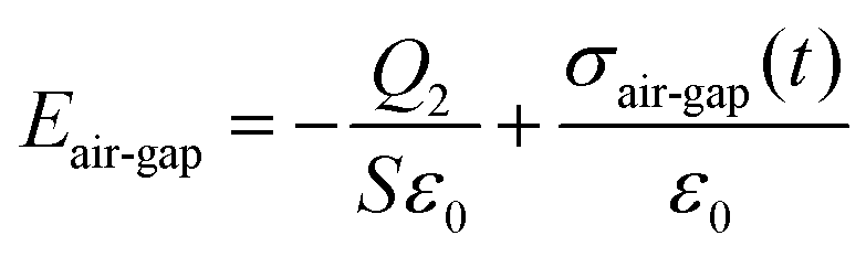 | (6) |
Due to its inherently formed microstructure of the sandpaper, the AE-TENG can generate a larger amount of the transferred charge than the normal TENG. Therefore, the value of Q2 is higher than Q1. Subsequently, the potential difference (VAE) can be given by the following equation.
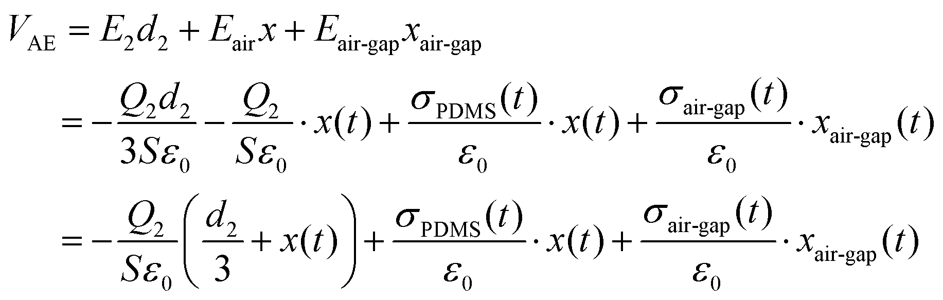 | (7) |
As a result, the AE-TENG can produce a higher potential difference between the electrodes than that of the normal TENG because of the air-gap induced triboelectric effect in the AE-TENG. It should be noted that this air-gap induced triboelectric effect can generate the additional electric field, which shows the same direction with the originally existing electric field between the top and bottom layers. Hence, this additional electric field enables the electrical output of the AE-TENG to be further enhanced. It could be considered that the induced charges in the air-gap were created by the repeated cycle of the existence and absence of the air-gap in the non-contact layer with the following operation procedure. (1) When a mechanical input is applied, the top layer approaches the bottom layer, including the PDMS layer and bottom electrode. (2) After a contact between the top layer and the bottom layer, the air-gap between the dielectric layer and the bottom electrode disappears simultaneously. (3) Subsequently, the following separation allows the air-gap between the dielectric layer and bottom electrode to be restored. In other words, repeating the contact-separation process in the non-contact layer allows for surface charges to be increasingly accumulated on the surface inside the air-gap, enabling the increase in the electrical output of the AE-TENG.
To quantitatively compare the electrical performances among the four types of TENGs, the basic output characteristics, which include the amount of transferred charges (Qtr), the open-circuit voltage (VOC), and the short-circuit current (ISC), were measured from the four fabricated TENGs under the same applied force of 30 N and vibration frequency of 3 Hz, as shown in Fig. 4b–d, respectively. The structured AE-TENG generated the highest outputs of 111.1 nC, 59.2 V, and 4.54 μA. Otherwise, the normal TENG exhibited the lowest value of 60.4 nC, 24.4 V, and 1.3 μA. Also, the structured TENG showed 71.2 nC, 34.2 V, 2.08 μA, and AE-TENG generated the electrical outputs of 92 nC, 45.2 V, 4.03 μA.
The electrical outputs were highly influenced by the presence of the structured layer accompanying by the air-gap created by the sandpaper. The structured TENG is one of the representative models that contains an enhanced surface area by modifying the contact surface. Herein, the effective contact area was enlarged by using the top layer with the polished and Al-coated electrode. Therefore, the triboelectric charges can be accumulated more on the contact surface, which not only leads to the formation of a higher electric potential difference between the two electrodes, but allows for a larger amount of current to flow than that from the normal TENG. In the case of the AE-TENG, the electrical outputs were enhanced relative to that of the normal TENG, as described with the VAE equation above. In comparison with the structured TENG, the AE-TENG showed an increased charge output (Qtr), as shown in Fig. 4b. This result implied that the added number of accumulated charges at the air-gap in the AE-TENG is higher than the number of accumulated charge at the contact surface of the structured TENG. Therefore, the VOC and ISC showed higher outputs in the AE-TENG compared to the structured TENG with the same trend of Qtr in Fig. 4c and d, respectively. The structured AE-TENG with the combined structure of the structured TENG and AE-TENG generated the enhanced triboelectric charges on the structured surface of the top layer, as well as the air-gap induced triboelectric effect. The structured AE-TENG produced the highest electrical outputs among the suggested four kinds of TENGs.
To verify the electric potential distribution of the four types of TENGs, the finite element method (FEM) simulation tool (COMSOL Multiphysics) was used for visualizing the analytical modeling results. As shown in Fig. 4e, the results from the simulation also confirmed that the same tendency of the electric potential distribution with the measured electrical outputs was displayed by changing the type of TENGs. It is noteworthy that the structured AE-TENG generated the largest electric potential difference between two electrodes.
In addition, the output voltage, current, and power density of the four types of TENGs with different load resistances ranging from 100 Ω to 4 GΩ were investigated, and the results are shown in Fig. 5a and b. By Ohm's law, the output current was decreased as the load resistance increased, whereas the output voltage showed the opposite tendency to the output current, as shown in Fig. 5a. Additionally, the output power was calculated by the equation P = V2/R. V and R are the measured output voltage and load resistance, respectively. The power density value was attained by dividing the output power with the contact area of 22.5 cm2. Among the four types of TENGs, the structured AE-TENG generated the largest output power of 181 μW at 10 MΩ, indicating the input resistance of this nanogenerator. The structured AE-TENG also showed the faster and higher charging ability, as shown in Fig. 5c. The electrical outputs from the four types of TENGs were rectified and charged to a 0.1 μF capacitor. To reach the voltage of the capacitor to 10 V, the charging times by using the normal TENG, structured TENG, AE-TENG, and structured AE-TENG were measured at 27, 18, 11, and 9 seconds, respectively. It is noteworthy that the structured AE-TENG represented not only the outstanding electrical output performance, but the distinguished charging characteristic among other types of TENGs.
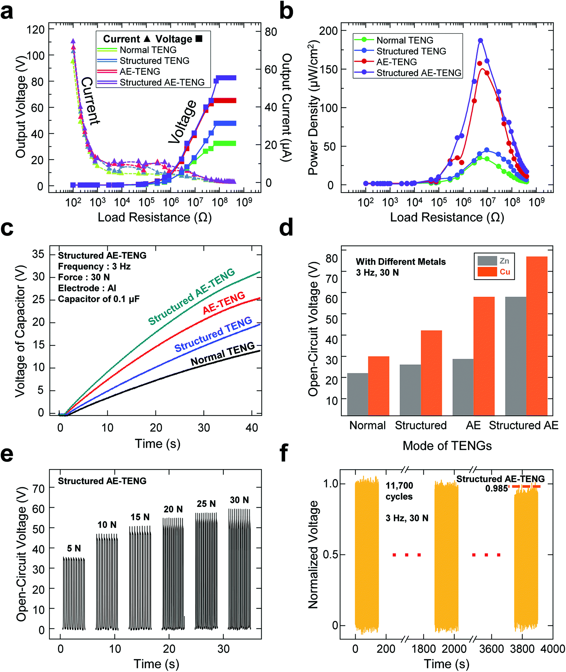 | ||
| Fig. 5 (a) The output voltage, output current, and (b) power density of the four types of TENGs with different load resistances ranging from 100 Ω to 0.4 GΩ. (c) The output voltage of the 0.1 μF commercial capacitor charged by the four types of TENGs. (d) Comparison of the open-circuit voltage (VOC) of the Cu and Zn-based four types of TENG. (e) The open-circuit voltage (VOC) of the structured AE-TENG under the different applied forces ranging from 5 N to 30 N. (f) The long-term durability test of the structured AE-TENG for seven days. | ||
Fig. 5d displays the VOC of the four types of TENGs with different metal electrodes, such as Zn or Cu. The tendency of the peak intensity from the four types of TENGs was maintained with changing the electrode material with the Zn and Cu electrodes in Fig. 5d, and even with the Al electrode in Fig. 4c. The VOC of the TENGs with the Cu electrode showed higher value than the TENGs with the Zn electrode consistently due to the higher conductivity of the Cu compared to that of the Zn. With changing the substrate from the PI film to the PTFE film, the electrical outputs were also checked and showed an increasing tendency in the order of the normal TENG, structured TENG, AE-TENG, and structured AE-TENG, regardless of the two input forces in Fig. S3.† These outputs showed consistency in the same increasing trend with this order when using different electrodes and substrates. When comparing with the electrical outputs using the PTFE or PI substrates, the PTFE substrate-case generated higher electrical outputs than that of the PI substrate-case. The electrical outputs from the TENG are proportional to the contact surface area. The PTFE substrate-case with the lower Young's modulus of 0.54 GPa can enlarge the contact area with the PDMS layer than the PI substrate-case with the higher Young's modulus of 2.5 GPa.56,57 In fabricating the AE-TENG, a trade-off relation needs to be considered in selecting the substrate material with the rigid and self-sustaining PI film, or the soft and high-output PTFE film.
Fig. 5e shows the VOC with varying the applied forces from 5 N to 30 N at the structure AE-TENG. By escalating the input forces, the peak-to-peak values of the VOC were also increased by virtue of the enlarged effective contact area. As previously mentioned in Fig. 3a and b, the applied force is highly related to the triboelectric effect. The strongly applied force can lead to the full contact-separation process in the non-contact layer, as well as the contact layer.
To confirm the output durability and reliability of the structured AE-TENG, this fabricated device was operated under the repeated vertical 3 Hz-input, as shown in Fig. 5f. The VOC of the structured AE-TENG was measured for seven days with the applied force of 30 N. The structured AE-TENG showed noticeable durability under high stimuli during this long-term operation. Even after going through the 11700 cycles of the contact-separation process, the VOC of the structured AE-TENG only decreased to 98.5% compared to the initial state. The intermittent operating test was also conducted with a period of 21 days. The electrical output was consistent during this period, as shown in Fig. S4.† This durability test represented the stable state of the TENG device after the mechanical deformation. It is notable that the test result could have resulted from the air-gap structure in the structured AE-TENG. For the reason that the air-gap between the dielectric layer and the metal layer prevented the abrasion of the contact layers from the external force, the electrical output could be maintained by the minimally damaged structure from the retained gap distance before and after the stability test in Fig. S5.† By adopting the air-gap existing structure to the vertical contact-separation TENG, not only the enhanced surface charge density, but also the structural protection ability can be achieved in comparison to the conventional TENG without the air-gap.
4. Conclusions
In summary, the air-gap embedded triboelectric nanogenerator, which effectively enhanced the electrical output from the triboelectric nanogenerator, was demonstrated with its additional electric field at the non-contact region arisen from the inherent air-gap between the dielectric layer and the electrode layer by using commercial sandpapers. The existence of the air-gap was verified using SEM images with the cross-sectional view. The four types of TENGs (normal TENG, structured TENG, AE-TENG, and structured AE-TENG) were systematically investigated with the aid of the theoretical model and measured electrical output characteristics. In the case of the structured TENG, the microstructured surface was fabricated on the top electrode, whereas the microstructure of the AE-TENG was fabricated on the bottom electrode. Lastly, the structured AE-TENG contained the modified structure layer on both top and bottom layers from the structured TENG and AE-TENG, respectively. The effect of the air-gap induced triboelectric effect was demonstrated by theoretical and computational modeling based on the V–Q–x relationship and software simulation. Through the electrical output measurement, the AE-TENG generated an enhanced power density with 156.8 μW cm−2, which was increased approximately four-fold compared to the power density from other TENGs of the normal (33.8 μW cm−2) or structured TENG (44.1 μW cm−2). The improved surface charge density and existence of an additional electric field enhanced the electrical output power of the AE-TENG. In addition, the structured AE-TENG, which has the combined structure of the structured TENG and AE-TENG, generated the highest electrical power of 204 μW cm−2. The increased dimension of the effective contact area induced a greater charge flow through the external load and more surface charges on the TENG-contact surface. Consequently, the enhancement of the electrical outputs was due to the effect of a microstructure formed on the non-contact and contact surfaces. The reason for the higher electrical outputs of the AE-TENG compared to the normal TENG and structured TENG was the presence of the air-gap, which caused an additional triboelectric effect at the non-contact layer in the bottom layer of the AE-TENG. This approach using an air-gap of the non-contact layer for improving the electrical performance of the contact-separation mode TENGs can be expected to contribute to the structural development of the TENG research, even during the long-time operation with this simple, cost-effective, and less time-consuming surface modification method.Author contributions
Inkyum Kim organized and integrated the acquired data, and wrote the original draft and documents for reviewing. Hyeonhee Roh conducted the formal analysis and analyzed the data with software. Wontae Choi found the methodology for conducting the experiments. Daewon Kim conceptualized the research idea, and supervised the validation of the research and writing documents for review and editing.Conflicts of interest
There are no conflicts to declare.Acknowledgements
This research was supported by the Basic Science Research Program through the National Research Foundation of Korea (NRF) funded by the Ministry of Education (2018R1A6A1A03025708). This research was supported by the National R&D Program through the National Research Foundation of Korea (NRF) funded by the Ministry of Science and ICT (No. 2020M3H2A1076786).References
- Y.-F. Lin, J. Song, Y. Ding, S.-Y. Lu and Z. L. Wang, Appl. Phys. Lett., 2008, 92, 022105 CrossRef.
- D. E. Carlson and C. R. Wronski, Appl. Phys. Lett., 1976, 28, 671–673 CrossRef CAS.
- S. B. Riffat and X. Ma, Appl. Therm. Eng., 2003, 23, 913–935 CrossRef.
- S. P. Beeby, R. N. Torah, M. J. Tudor, P. Glynne-Jones, T. O'Donnell, C. R. Saha and S. Roy, J. Micromech. Microeng., 2007, 17, 1257–1265 CrossRef.
- S. Wang, L. Lin and Z. L. Wang, Nano Energy, 2015, 11, 436–462 CrossRef CAS.
- Z. L. Wang, T. Jiang and L. Xu, Nano Energy, 2017, 39, 9–23 CrossRef CAS.
- R. G. Horn, D. T. Smith and A. Grabbe, Nature, 1993, 366, 442–443 CrossRef CAS.
- R. G. Horn and D. T. Smith, Science, 1992, 256, 362–364 CrossRef CAS PubMed.
- L. S. McCarty and G. M. Whitesides, Angew. Chem., Int. Ed., 2008, 47, 2188–2207 CrossRef CAS PubMed.
- H. T. Baytekin, A. Z. Patashinski, M. Branicki, B. Baytekin, S. Soh and B. A. Grzybowski, Science, 2011, 333, 308–312 CrossRef CAS PubMed.
- S. Wang, L. Lin, Y. Xie, Q. Jing, S. Niu and Z. L. Wang, Nano Lett., 2013, 13, 2226–2233 CrossRef CAS PubMed.
- H. Yang, W. Liu, Y. Xi, M. Lai, H. Guo, G. Liu, M. Wang, T. Li, X. Ji and X. Li, Nano Energy, 2018, 47, 539–546 CrossRef CAS.
- R. K. Cheedarala, A. N. Parvez and K. K. Ahn, Nano Energy, 2018, 53, 362–372 CrossRef CAS.
- M. A. P. Mahmud, J. J. Lee, G. H. Kim, H. J. Lim and K. B. Choi, Microelectron. Eng., 2016, 159, 102–107 CrossRef CAS.
- H. Zhang, L. Quan, J. Chen, C. Xu, C. Zhang, S. Dong, C. Lü and J. Luo, Nano Energy, 2019, 56, 700–707 CrossRef CAS.
- T. Guo, G. Liu, Y. Pang, B. Wu, F. Xi, J. Zhao, T. Bu, X. Fu, X. Li, C. Zhang and Z. L. Wang, Extreme Mech. Lett., 2018, 18, 1–8 CrossRef.
- S. Niu, Y. Liu, X. Chen, S. Wang, Y. S. Zhou, L. Lin, Y. Xie and Z. L. Wang, Nano Energy, 2015, 12, 760–774 CrossRef CAS.
- G. Zhu, J. Chen, Y. Liu, P. Bai, Y. S. Zhou, Q. Jing, C. Pan and Z. L. Wang, Nano Lett., 2013, 13, 2282–2289 CrossRef CAS PubMed.
- D. Lee and D. Kim, Nano Energy, 2020, 71, 104599 CrossRef CAS.
- Z. L. Wang, Faraday Discuss., 2014, 176, 447–458 RSC.
- H. Zhang, Y. Yang, T.-C. Hou, Y. Su, C. Hu and Z. L. Wang, Nano Energy, 2013, 2, 1019–1024 CrossRef CAS.
- Y. Yang, H. Zhang, Z.-H. Lin, Y. S. Zhou, Q. Jing, Y. Su, J. Yang, J. Chen, C. Hu and Z. L. Wang, ACS Nano, 2013, 7, 9213–9222 CrossRef CAS PubMed.
- Z. L. Wang, ACS Nano, 2013, 7, 9533–9557 CrossRef CAS PubMed.
- F. R. Fan, W. Tang and Z. L. Wang, Adv. Mater., 2016, 28, 4283–4305 CrossRef CAS PubMed.
- H. Yang, M. Deng, Q. Zeng, X. Zhang, J. Hu, Q. Tang, H. Yang, C. Hu, Y. Xi and Z. L. Wang, ACS Nano, 2020, 14, 3328–3336 CrossRef CAS PubMed.
- H. Yang, M. Deng, Q. Tang, W. He, C. Hu, Y. Xi, R. Liu and Z. L. Wang, Adv. Energy Mater., 2019, 9, 1901149 CrossRef.
- J. Chun, J. W. Kim, W.-S. Jung, C.-Y. Kang, S.-W. Kim, Z. L. Wang and J. M. Baik, Energy Environ. Sci., 2015, 8, 3006–3012 RSC.
- X.-S. Zhang, M.-D. Han, R.-X. Wang, B. Meng, F.-Y. Zhu, X.-M. Sun, W. Hu, W. Wang, Z.-H. Li and H.-X. Zhang, Nano Energy, 2014, 4, 123–131 CrossRef CAS.
- P. Bai, G. Zhu, Y. S. Zhou, S. Wang, J. Ma, G. Zhang and Z. L. Wang, Nano Res., 2014, 7, 990–997 CrossRef CAS.
- G. Song, Y. Kim, S. Yu, M.-O. Kim, S.-H. Park, S. M. Cho, D. B. Velusamy, S. H. Cho, K. L. Kim, J. Kim, E. Kim and C. Park, Chem. Mater., 2015, 27, 4749–4755 CrossRef CAS.
- J. Chun, B. U. Ye, J. W. Lee, D. Choi, C.-Y. Kang, S.-W. Kim, Z. L. Wang and J. M. Baik, Nat. Commun., 2016, 7, 12985 CrossRef CAS PubMed.
- H. Roh, I. Kim and D. Kim, Nano Energy, 2020, 70, 104515 CrossRef CAS.
- Y. Liu, W. Liu, Z. Wang, W. He, Q. Tang, Y. Xi, X. Wang, H. Guo and C. Hu, Nat. Commun., 2020, 11, 1599 CrossRef CAS PubMed.
- W. He, W. Liu, J. Chen, Z. Wang, Y. Liu, X. Pu, H. Yang, Q. Tang, H. Yang, H. Guo and C. Hu, Nat. Commun., 2020, 11, 4277 CrossRef CAS PubMed.
- J. Chen, H. Guo, X. He, G. Liu, Y. Xi, H. Shi and C. Hu, ACS Appl. Mater. Interfaces, 2016, 8, 736–744 CrossRef CAS PubMed.
- D. W. Kim, J. H. Lee, I. You, J. K. Kim and U. Jeong, Nano Energy, 2018, 50, 192–200 CrossRef CAS.
- H.-W. Park, N. D. Huynh, W. Kim, C. Lee, Y. Nam, S. Lee, K.-B. Chung and D. Choi, Nano Energy, 2018, 50, 9–15 CrossRef CAS.
- D. Park, S. Lee, C. V. Anh, P. Park and J. Nah, Nano Energy, 2019, 55, 501–505 CrossRef CAS.
- F.-R. Fan, L. Lin, G. Zhu, W. Wu, R. Zhang and Z. L. Wang, Nano Lett., 2012, 12, 3109–3114 CrossRef CAS PubMed.
- X.-S. Zhang, M.-D. Han, R.-X. Wang, F.-Y. Zhu, Z.-H. Li, W. Wang and H.-X. Zhang, Nano Lett., 2013, 13, 1168–1172 CrossRef CAS PubMed.
- D. Yoo, E. Y. Go, D. Choi, J.-W. Lee, I. Song, J.-Y. Sim, W. Hwang and D. S. Kim, Nanomaterials, 2019, 9, 71 CrossRef PubMed.
- L. Zhao, Q. Zheng, H. Ouyang, H. Li, L. Yan, B. Shi and Z. Li, Nano Energy, 2016, 28, 172–178 CrossRef CAS.
- J. Gong, B. Xu and X. Tao, ACS Appl. Mater. Interfaces, 2017, 9, 4988–4997 CrossRef CAS PubMed.
- X. Li, C. Xu, C. Wang, J. Shao, X. Chen, C. Wang, H. Tian, Y. Wang, Q. Yang, L. Wang and B. Lu, Nano Energy, 2017, 40, 646–654 CrossRef CAS.
- X.-W. Zhang, G.-Z. Li, G.-G. Wang, J.-L. Tian, Y.-L. Liu, D.-M. Ye, Z. Liu, H.-Y. Zhang and J.-C. Han, ACS Sustainable Chem. Eng., 2018, 6, 2283–2291 CrossRef CAS.
- S. Jin, Y. Wang, M. Motlag, S. Gao, J. Xu, Q. Nian, W. Wu and G. J. Cheng, Adv. Mater., 2018, 30, 1705840 CrossRef PubMed.
- S. He, Z. Yu, H. Zhou, Z. Huang, Y. Zhang, Y. Li, J. Li, Y. Wang and D. Li, Nano Energy, 2018, 52, 134–141 CrossRef CAS.
- G. Yao, L. Xu, X. Cheng, Y. Li, X. Huang, W. Guo, S. Liu, Z. L. Wang and H. Wu, Adv. Funct. Mater., 2020, 30, 1907312 CrossRef CAS.
- M. Zhu, Y. Wang, M. Lou, J. Yu, Z. Li and B. Ding, Nano Energy, 2021, 81, 105669 CrossRef CAS.
- A. R. Mule, B. Dudem and J. S. Yu, Energy, 2018, 165, 677–684 CrossRef CAS.
- J. H. Lee, I. Yu, S. Hyun, J. K. Kim and U. Jeong, Nano Energy, 2017, 34, 233–241 CrossRef CAS.
- S. Li, D. Huang, B. Zhang, X. Xu, M. Wang, G. Yang and Y. Shen, Adv. Energy Mater., 2014, 4, 1301655 CrossRef.
- S. Niu, S. Wang, L. Lin, Y. Liu, Y. S. Zhou, Y. Hu and Z. L. Wang, Energy Environ. Sci., 2013, 6, 3576–3583 RSC.
- R. Hinchet, A. Ghaffarinejad, Y. Lu, J. Y. Hasani, S.-W. Kim and P. Basset, Nano Energy, 2018, 47, 401–409 CrossRef CAS.
- J. Shao, M. Willatzen and Z. L. Wang, J. Appl. Phys., 2020, 128, 111101 CrossRef CAS.
- P. J. Rae and D. M. Dattelbaum, Polymer, 2004, 45, 7615–7625 CrossRef CAS.
- W.-Y. Chang, T.-H. Fang and Y.-C. Lin, Appl. Phys. A: Mater. Sci. Process., 2008, 92, 693–701 CrossRef CAS.
Footnote |
| † Electronic supplementary information (ESI) available. See DOI: 10.1039/d1nr01517f |
| This journal is © The Royal Society of Chemistry 2021 |