
Recent advances in optical and optoelectronic data storage based on luminescent nanomaterials
Jinbo
Yu
 ab,
Mingtao
Luo
c,
Ziyu
Lv
a,
Shenming
Huang
d,
Hsiao-Hsuan
Hsu
e,
Chi-Ching
Kuo
f,
Su-Ting
Han
*a and
Ye
Zhou
*c
ab,
Mingtao
Luo
c,
Ziyu
Lv
a,
Shenming
Huang
d,
Hsiao-Hsuan
Hsu
e,
Chi-Ching
Kuo
f,
Su-Ting
Han
*a and
Ye
Zhou
*c
aInstitute of Microscale Optoelectronics, Shenzhen University, 3688 Nanhai Road, Shenzhen, 518060, P.R. China. E-mail: sutinghan@szu.edu.cn
bKey Laboratory of Optoelectronic Devices and Systems of Ministry of Education and Guangdong Province, College of Optoelectronic Engineering, Shenzhen University, Shenzhen, 518060, P. R. China
cInstitute for Advanced Study Shenzhen University, Shenzhen 518060, P. R. China. E-mail: yezhou@szu.edu.cn
dSchool of Electronics and Information Engineering, Shenzhen University, 3688 Nanhai Road, Shenzhen, 518060, P.R. China
eDepartment of Materials and Mineral Resources Engineering, National Taipei University of Technology, Taipei, Taiwan
fInstitute of Organic and Polymeric Materials, Research and Development Center of Smart Textile Technology, National Taipei University of Technology, Taipei, Taiwan
First published on 9th November 2020
Abstract
The substantial amount of data generated every second in the big data age creates a pressing requirement for new and advanced data storage techniques. Luminescent nanomaterials (LNMs) not only possess the same optical properties as their bulk materials but also have unique electronic and mechanical characteristics due to the strong constraints of photons and electrons at the nanoscale, enabling the development of revolutionary methods for data storage with superhigh storage capacity, ultra-long working lifetime, and ultra-low power consumption. In this review, we investigate the latest achievements in LNMs for constructing next-generation data storage systems, with a focus on optical data storage and optoelectronic data storage. We summarize the LNMs used in data storage, namely upconversion nanomaterials, long persistence luminescent nanomaterials, and downconversion nanomaterials, and their applications in optical data storage and optoelectronic data storage. We conclude by discussing the superiority of the two types of data storage and survey the prospects for the field.
 Jinbo Yu | Dr Jinbo Yu received his Ph.D. degree from the school of chemistry at Sun Yat-sen University in 2018. He is now a postdoctoral fellow at the Institute of Microscale Optoelectronics at Shenzhen University, focusing on luminescent nanomaterials and their application in memory devices, mainly including memristors, flash memory, and in-memory computing. |
 Mingtao Luo | Ming-Tao Luo is currently an undergraduate student in his senior year at the Institute for Advanced Study at Shenzhen University, Guangdong, China. He majors in Physics at Shenzhen University. His research interests are organic/inorganic semiconductors and organic/inorganic materials for nanoscale devices, such as optical and optoelectronic data storage. |
 Ziyu Lv | Dr Ziyu Lv received his Ph.D. degree from the State Key Laboratory of Advanced Technology for Materials Synthesis and Processing at Wuhan University of Technology in 2017. He was a postdoctoral fellow at Shenzhen University from 2017 to 2018. He is presently an associate research fellow in the Institute of Microscale Optoelectronics at Shenzhen University, focusing on nonvolatile memory and biomaterials-based electronics, mainly including memristive devices, flash memory, neuromorphic computing systems, protein/peptide-based bioelectronics devices, and their applications. |
 Shenming Huang | Shenming Huang received his B.S. degree from the College of Electronic Engineering, South China Agricultural University (2019). He is presently a postgraduate student in the College of Electronics and Information Engineering, Shenzhen University. His research interests are artificial synapses and flexible electronics. |
 Su-Ting Han | Prof. Su-Ting Han is an associate professor at Shenzhen University. She received her MSc degree in Analytical Chemistry from Hong Kong Baptist University and her PhD degree in Physics and Materials Science from City University of Hong Kong. After graduation, she worked at the City University of Hong Kong as a postdoctoral fellow. Her research interests include functional electronic devices and flexible, stretchable, and wearable electronics. |
 Ye Zhou | Prof. Ye Zhou is an IAS Fellow and group leader in the Institute for Advanced Study, Shenzhen University. His research interests include flexible and printed electronics, organic/inorganic semiconductors, surface and interface physics, nanostructured materials, and nano-scale devices for technological applications, such as logic circuits, data storage, photonics and sensors. |
Introduction
Humanity is progressing toward an age of data explosion; the Internet of Things (IoT), mobile technology and artificial intelligence (AI) have been developing rapidly in recent years.1 The latest white paper from International Data Corporation (IDC) predicts that by 2025, the total amount of data will reach 175 ZB.2 Additionally, these data will still need to be continuously stored and easily accessed over the decades. These stringent demands create an insurmountable challenge for existing data centers that are composed of magnetic hard-disk drives, which may have a lifetime of only two years and will consume about one-fifth of the world's electricity by 2025.3 The massive amount of digital data generated from the IoT, mobile technology, and AI is stimulating the sustained upgrade of storage modes and mediums.4–7 To date, data storage involving magnetic materials has been gradually replaced by optical data storage and optoelectronic data storage, which possess higher efficiency, lower energy consumption, higher security, higher capacity, and longer lifetimes.8However, traditional optical and electronic data storage (e.g., flash memory and memristive memory) still have shortcomings in storage capacity; therefore, it is difficult to store the large amounts of data generated every day in the age of data explosion.6,9–11 LNMs offer more ways to increase the capacity of traditional optical and electronic data storage and create solutions with tremendous potential. The advent of nanophotonics has offered new pathways for light-matter interaction, allowing nanoscale-manipulated operation of materials by employing light.12–17 Implementing optical and optoelectronic data storage employing LNMs with their tailorable optoelectrical characteristics can result in continuous improvement in data storage for sustainable growth.
Optical data storage combined with microscopy technologies has a powerful advantage over contemporary approaches because it has been acknowledged to have advantages in the matter of performance and durability. However, it is difficult to enable a large hike in the capacity of currently available data storage devices. Additionally, a fundamental limitation imposed by far-field diffraction physics creates a great restriction on the current state-of-the-art in optical storage data. Therefore, more improvements should be developed through the use of far-field evanescent radiation and/or promoting the technology from two-dimensional (2D) surface operations to three-dimensional (3D) volumetric implementations. As a consequence, it is necessary to break through the diffraction limit to achieve optical data storage at the nanoscale. The rise of femtosecond laser direct writing technology with unique 3D processing ability, arbitrary-form designability, and as many as tens of nanometers of superhigh fabrication accuracy (far exceeding the optical diffraction limit) offers a new way to break the diffraction limit barrier and bring about a renaissance of high-capacity optical data storage.18,19
Optoelectronic data storage, which can realize electrical information programming and optical information programming operations at the same time, can significantly increase the capacity of data storage compared to traditional electronic data storage.20,21 Moreover, it lowers the operation voltage by inducing light into the devices, meanwhile reducing the consumption of electricity. However, conventional single active layer-based devices usually suffer from low electron mobility, high operation voltage, and low light response, which imposes restrictions on developing high-performance and high-capacity data storage devices.22–24 The application of nanomaterials in optoelectronic data storage may solve the problems mentioned above.
Innovative evolution in the field of nanotechnology has brought about the development of many new nanomaterials that are essential alternative options for application in memory devices. The scale of LNMs enables the use of one or several nanoparticles (NPs) as data write-in units. Compared with their bulk counterparts, LNMs reveal unique optical, electronic, and mechanical properties, and photons/electrons can be strongly confined at the nanoscale.25–28 Due to their wide absorption bandwidths, high efficiencies of down-conversion and up-conversion, different luminescence lifetimes, superhigh light resistance stability, and non-light-bleaching characteristics, LNMs are an optimal choice for fabricating optical data storage devices by far-field-super-resolution techniques.19,29,30 Moreover, the good dispersibility of LNMs in water and almost all organic solvents facilitates their incorporation into host matrices for the mass production of low-cost optical and optoelectronic data storage devices.31,32
In this review, we concentrate on recent achievements in LNMs used in current data storage systems, as depicted in Fig. 1. First, we give a comprehensive review of the progress in the field of optical data storage and the types of inorganic LNMs employed in developing optical data storage. Then, we describe various kinds of optoelectronic data storage and the types of inorganic LNMs utilized in optoelectronic data storage. Finally, we briefly discuss the advantages and disadvantages of these two kinds of data storage and give the prospects of each kind in different fields of data storage.
 | ||
| Fig. 1 LNM-based data storage-optical data storage and optoelectronic data storage devices. | ||
Optical data storage
The luminescence processes of luminescent materials can be divided into four main types: long persistent luminescence, down-conversion luminescence, up-conversion luminescence, and quantum cutting luminescence. Unfortunately, almost no quantum cutting luminescent nanomaterials are suitable to fabricate optical and optoelectrical data storage because of the shortage of nanomaterials with visible quantum cutting luminescence and sensitive near-infrared light response materials. Therefore, only three of the luminescence types are used for fabricating optical data storage systems. With the rapid development of nanotechnology, STED (stimulated emission depletion) nanoscopy, and femtosecond laser direct writing, recent achievements in the area of optical data storage on the basis of photostimulated luminescence, down-conversion luminescence, and up-conversion luminescence are summarized as follows:Optical data storage based on photostimulated luminescence
Long persistent luminescent materials (LPLMs) with photo-stimulated luminescence are a unique family of advanced luminescent materials which possess excellent ability to store photons under exposure to short-wavelength light and to sustain glow even after removing the excitation light source. Key factors involved in the luminescence mechanism of long persistent materials are the processes of charge carrier trapping and de-trapping, which realize the processes of storage and release of photons in LPLMs. The trap depth in the LPLMs and the releasing activation energy of the captured charge carriers have a great influence on the probability of charge carrier trapping and de-trapping.34 The low traps of LPLMs have been adopted in different areas of daily life. Common room-temperature (RT) LPLMs with low trapping depths of 0.5–0.8 eV, such as SrAl2O4:Eu,Dy, and ZnGa2O4:Cr, are widely applied in security signs for dark conditions,35 AC-solid-state lighting,36 and in vivo bioimaging.37–39 However, for the photons trapped in the deep traps of the materials, it is relatively difficult to achieve the de-trapping process at RT; therefore, LPLMs are not commonly involved in the applications mentioned above. Fortunately, if we employ the trapping and de-trapping processes of the deep traps in LPLMs at RT as data write-in and data read-out under additional stimulation, the deep traps in LPLMs can thus be applied in high-capacity optical data storage. Because the photons that emerge from different deep traps show particular spectral properties, the photon trap and de-trap modes can achieve multi-level data storage processes by multiplexing a variety of spectral information. The proposed mechanism of the photon storage and release processes in LPLMs is shown in Fig. 2a.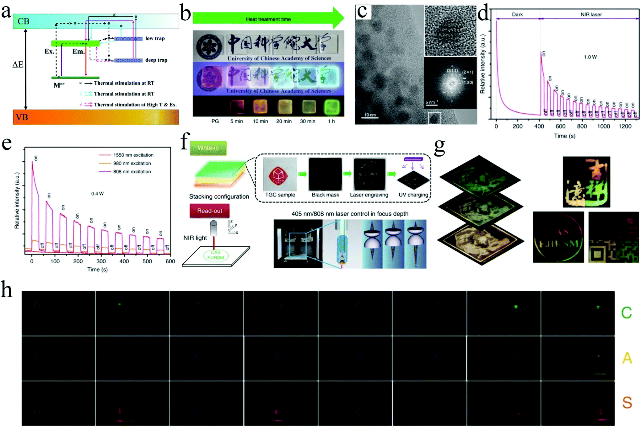 | ||
| Fig. 2 (a) Schematic of the mechanism of the photon storage and release processes in LPLMs. (b) Photographs of the PG and TGC under daylight (up), UV light (254 nm) for 5 min (middle), and UV light (254 nm) for 5 min in advance and after thermal stimulation (bottom). (c) The high-resolution transmission electron microscopy (HRTEM) results of the TGC. Photoluminescence (PL) decay curves of TGC excited by (d) the 1 W NIR laser (λex = 808 nm) and (e) stimulated by different wavelengths of 0.4 W NIR laser (λem = 510 nm, on/off intervals: 30 s). (f) Schematic of multi-level optical data storage and the data write-in/read-out process. (g) The 3D data readouts of the different encoded images embedded in different layers and wavelength multiplexing by incorporation with four kinds of TGCs with the aid of heat treatment. (h) Photograph of the 3D optical data read-out processes realized by a NIR laser (λex = 808 nm, power density: 1.3 W mm−2) to exhibit the encoded English letters of a defined binary system. Reproduced with permission.33 Copyright 2020, Springer Nature. | ||
Previous studies have reported numerous optical data storage technologies based on long persistent bulk phosphors. These optical data storage systems are fabricated by dispersing bulk phosphors in glass, ceramic, or organic hosts, which creates low capacity or stability issues.34,40–42 To highly improve the capacity and stability of optical data storage based on LPLMs, new technologies (e.g., nanotechnology, femtosecond laser direct writing technology, and transparent glass-ceramics synthetic technology) offer a new approach to achieve higher capacity and stability of optical data storage. Lin et al. developed a novel optical data storage system consisting of transparent glass-ceramic (TGC) containing uniformly dispersed photostimulated nanocrystals (LiGa5O8:Mn2+); they successfully achieved a bit-by-bit optical information write-in and read-out process in a photon trapping/de-trapping mode.33Fig. 2b shows digital pictures of the precursor glass (PG) and TGCs under different conditions, which provides powerful evidence that the LPLMs were made in the TGC. Then, further evidence from the high-resolution TEM observation and fast Fourier transform pattern revealed that monodispersed LiGa5O8 NPs were uniformly dispersed in the TGC (Fig. 2c). Fig. 2d and e show that the TGC embedded with LiGa5O8:Mn2+ nanocrystals provided a fast information read-out rate for optical data storage. Data write-in was realized by ablating the patterns by a 405 nm laser on TGC coated with black ink and then exposing the TGC to a UV light source (204 nm), while data read-out was achieved by stepwise NIR laser scanning in bit-by-bit mode, as shown in Fig. 2f. As demonstrated in Fig. 2g, wavelength and intensity multiplexing were efficient to improve the storage capacity of the LiGa5O8:Mn2+ nanocrystal-based optical data storage and were successfully realized by integrating different TGC species into one system obtained with various heat treatment times. Finally, the authors successfully realized a demonstration of 3D data storage in the multilayer TGC, which was performed by encoding the short name of the Chinese Academy of Science (CAS), as depicted in Fig. 2h.
Due to the unique structures of nano LPLMs and the low and deep traps of nanomaterials inside long persistent luminescent TGCs, these nanomaterials are preferred to their bulk phosphors, which is propitious to stimulate emission exhaustion methods for superhigh-resolution write-in and read-out in optical data storage applications. Particularly, a higher capacity of optical data storage can be achieved by utilizing progressive far-field super-resolution optical microscopy, which can easily break through the optical diffraction limit. It also provides a potential way to further achieve higher capacity optical data storage by wavelength and intensity multiplexing. Moreover, the trap energy levels of the LPLMs are serial and metastable, which reduces the energy consumption of the photon trapping and de-trapping process, enabling the realization of information write-in and read-out with ultra-low excitation power. TGCs with nano LPLMs show great stability under harsh working conditions and may serve as an ideal way to fabricate high-capacity, high-density and superhigh security optical data storage devices with ultralong lifetimes.
Optical data storage based on down-conversion luminescence
Down-conversion luminescent materials (DCLMs) can convert a photon with high energy into a photon with low energy, which is a typical process of converting a short-wavelength light into a long-wavelength light. Most DCLMs can realize the wavelength conversion of visible light by a down-conversion process, which offers more approaches to enlarge the applications of single-wavelength light, e.g. lighting, displaying, data projectors, optical wireless communication, and plant growth lighting.43,44 These applications of DCLMs are widely used in daily life and have significantly changed our lifestyle. Fortunately, with the accelerated innovation of nanotechnology, the nanocrystallization of DCLMs offers a new approach to expand the application of DCLMs to more areas, such as optical data storage and bioimaging.45,46 As with optical data storage, nano DCLMs are being gradually used and represent a substantial breakthrough in high-capacity optical data storage. To date, DCLMs have been employed for fabricating optical data storage in two ways. The first method is to make full use of the basic down-conversion luminescence characteristics of DCLMs. The second method is to take advantage of the luminescence spectra and lifetimes to realize multi-level and multidimensional optical data storage. Recently, the first method has attracted considerable attention as a simple method to easily realize data write-in and read-out by DCLM-based optical data storage on account of its excellent high down-conversion efficiency. Li et al. developed a rewritable “fluorescence” system based on branched polyethyleneimine (BPEI) quantum dots (QDs) with a multicolor recording mode, where BPEI acted as both a QD multicolor pattern “writer” and data erasure “remover” (Fig. 3a).47 Additionally, the authors successfully fabricated a binary coded two-color microarray data storage chip and achieved a write-in and read-out process, as presented in Fig. 3b. This low-cost solution-based manufacturing method and the use of nano QDs provided great potential for manufacturing multi-state memory chips, which could be widely used in anti-counterfeiting and secure communications. Gorbiak et al. reported that photosensitive glasses with silver-containing silicate photo-thermo-refractive materials could be used to enable multi-level optical information recording by utilizing UV nanosecond laser pulses.48 The data write-in could be achieved by the creation of silver NPs with plasmon resonance fabricated by nanosecond laser pulses, while the information read-out could be realized by lasers or LEDs (λex = 405 or 450 nm), as illustrated in Fig. 3c. Although the nano DCLMs used in the 2D optical data storage systems mentioned above greatly improved the capacity of nano DCLM-based optical data storage, 2D optical data storage is not the best way to reach the limit of nano DCLM-based optical data storage. Therefore, femtosecond laser direct writing realized by advanced laser technology on the nanoscale is feasible to produce 3D optical data storage, which is a low-cost and simple way to greatly improve the capacity of nano DCLM-based optical data storage. Huang et al. successfully developed a transparent glass medium containing CsPbBr3 QDs using a computer-controlled near-infrared femtosecond laser (λ = 800 nm); this process afforded a stable high-capacity 3D optical data storage device, as shown in Fig. 3d–f.49 Owing to the low formation energy of CsPbBr3 QDs, the 3D luminescent structure of the optical data storage device could be destroyed by the femtosecond laser and then reconstructed by annealing, as presented in Fig. 3e. Additionally, the size and PL intensity of the modified regions could be adjusted by changing the laser power density, exposure time of the laser, and moving speed of the sample stage. Due to these benefits, the CsPbBr3 QDs transparent glass showed great potential in enabling stable high-capacity 3D optical data storage, as depicted in Fig. 3f. As demonstrated in Fig. 3g, the CsPbBr3 QDs-based optical data storage exhibited excellent data storage stability after a 30-day polar solvent test. Then, Huang et al. demonstrated femtosecond-laser assisted creation of 3D CsPb(Cl/Br)3 nanocrystal patterns exhibiting bright blue PL inside oxide glass under UV light irradiation.52 Unlike the CsPbBr3 QDs transparent glass-based optical data storage mentioned above, the creation of 3D CsPb(Cl/Br)3 nanocrystal patterns in transparent glass, which could not be achieved by direct heat treatment, was realized by employing femtosecond laser irradiation followed by low-temperature heat treatment. Moreover, the strong blue PL from the CsPb (Cl/Br)3 nanocrystals could be fully shut down by further femtosecond laser illumination and turned on by the low-temperature heat treatment. These recoverable constructed regions inside the transparent glass medium showed great potential in stable high-capacity optical data storage and information security protection applications. The second method to enable high-capacity optical data storage has also made great progress. Riesen et al. reported multi-level optical data storage on the basis of the highly efficient formation of stable Sm2+ in BaFCl:Sm3+ nanocrystals by irradiation with deep UV (UV-C) below 250 nm.50 The data write-in process was realized by the UV-C-induced valence state-switching Sm3+ → Sm2+ process, while the data read-out process was carried out by the one-photon excited red PL of the Sm2+ in the blue-violet range. The multi-level encoding for 2D optical data storage was achieved by applying a simple CCD-camera-based imaging device with a relatively small numerical aperture which hence had low efficacy for photon focusing, as shown in Fig. 3h. The CCD-camera imaging device equipped with a large numerical aperture cooperating with a photodiode-based read-out or photomultiplier enabled the readout of 10× weaker optical signals. Then, Riesen et al. reported a proof-of-principle to confirm the realization of reversible encoding multi-level optical data storage in a single BaFCl:Sm3+ nanocrystal.53 By varying the UV-C light intensity for the Sm valence conversion to discretely change the valence state and by applying confocal optics to realize the PL intensity read-out, the concept of high-capacity optical data storage with a complete write-read-erase cycle was successfully realized. The discovery of reversible and highly efficient Sm valence state conversion within BaFCl:Sm3+ nanocrystals offered more approaches to obtain high-capacity optical data storage without using a femtosecond laser. Feng et al. reported a time-gate nano-hybrid on the basis of the variable Eu valence state acting as an active material in multi-level and multi-dimensional optical data storage devices.51 The nano-hybrid consisting of the variable Eu valence state, organic ligand, and m-SiO2 showed the ability to facilitate light stimuli-responsive and time-gated optical encryption and encoding in spatial and temporal dimensions, as shown in Fig. 3i. The nano-hybrid possessing dual response of light stimuli and time gates provided new options for the fabrication of high-capacity and high-security optical data storage.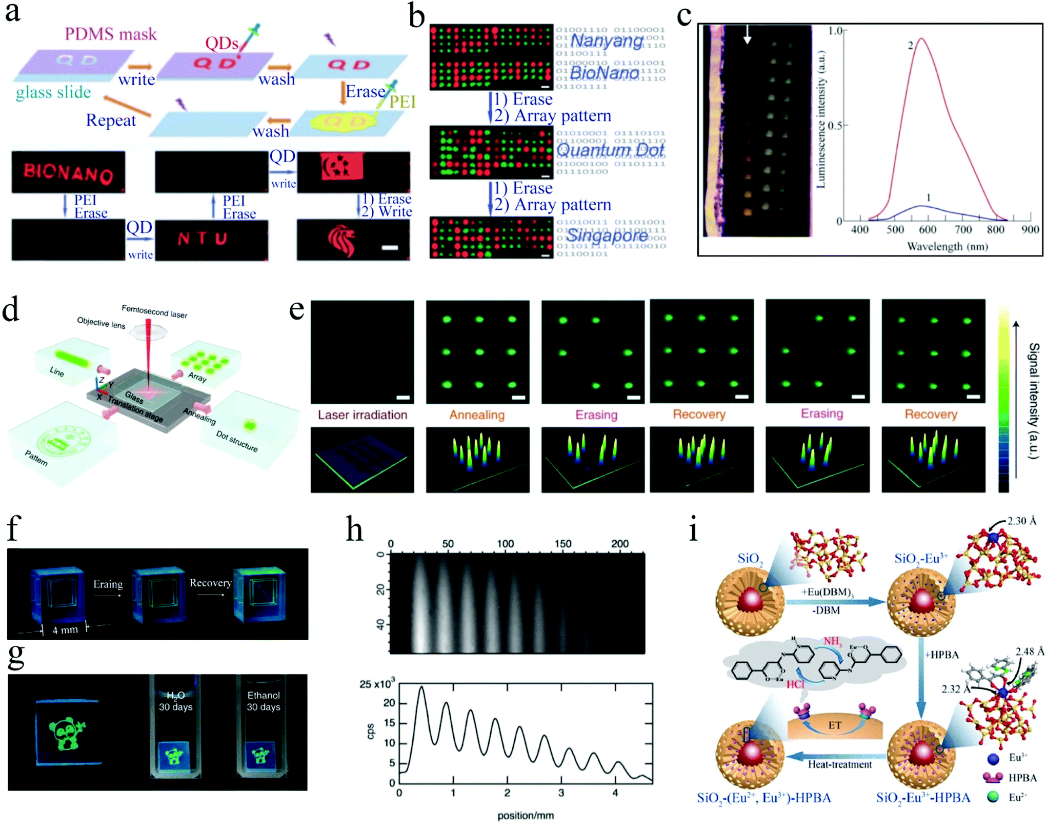 | ||
| Fig. 3 (a) Diagram of the data writing and erasing process of CdTe QDs-based optical data storage. (b) Demonstration of the reversible writing and erasing process by the binary-coded microarray consisting of red and green colors (scale bar: 30 mm). Reproduced with permission.47 Copyright 2011, Royal Society of Chemistry. (c) Photograph and photoluminescence of the irradiated zones in photo-thermo-refractive glass with a series of laser pulses from 1 to 10 (1–1 laser pulse, 2–10 laser pulses. λex = 405 nm). Reproduced with permission.48 Copyright 2017, SPIE. (d) Demonstration of the 3D XYZ-controlled femtosecond laser writing system for optical data storage. (e) Photographs (upper) and data read-out signal intensity mapping images (bottom) of a CsPbBr3 QD array during the reversible writing and erasing processes under UV light (scale bars: 100 μm). (f) Photographs of 3D multi-level data storage realized in a cubic transparent glass-ceramic sample. (g) The 30-day stability tests of CsPbBr3 QD patterns dipped into deionized water and ethanol. Reproduced with permission.49 Copyright 2020, Springer Nature. (h) The simple CCD camera-based imaging setup (upper) and the profile plot (bottom) of the multi-level encoding. Reproduced with permission.50 Copyright 2017, Optical Society of America. (i) Schematic of the multi-level data storage achieved in a time-gate nanohybrid on the basis of variable Eu valence. Reproduced with permission.51 Copyright 2019, American Chemical Society. | ||
Although femtosecond laser direct writing and proof-of-principle of reversible multi-level optical data storage have been reported for optical data storage based on DCLMs, they still suffer from the low fabrication efficiency of femtosecond laser direct writing, the low light conversion efficiency of DCLMs, fewer materials, and fewer photo-chemical mechanisms used in high-density optical data storage. However, with the continuous efforts being made to explore novel nanomaterials, optical information write-in and read-out technologies, and photo-chemical mechanisms, nano DCLM-based high-density and high-capacity optical data storage will have a bright future.
Optical data storage based on up-conversion luminescence (UCL)
UCL is also called anti-Stokes-type emission. Luminescent materials with UCL properties can absorb two or more low-energy photons and then convert the low-energy photons into high-energy photons, resulting in a shorter wavelength of emitting light than of exciting light; this is the opposite nonlinear optical phenomenon of down-conversion fluorescence. Excited states with long lifetimes and many intermediate energy levels are requisite for the realization of UCL. The characteristics mentioned above are commonly observed in the rare earth elements, consisting of the lanthanide series, yttrium, and scandium, such as Yb/Er, Yb/Tm, and Yb/Ho. Therefore, rare-earth-doped luminescent materials are well-known classical up-conversion luminescent materials which can respond to near-infrared excitation and then emit up-conversion PL, showing excellent characteristics such as parity forbidden 4f–4f transitions, long fluorescence lifetimes, and emissions with large anti-Stoke shifts. Fig. 4a shows the UCL process and energy diagram of NaYF4:Yb/Tm. Additionally, compared with other multi-photon absorption processes, such as double-photon absorption and second harmonic generation, rare-earth-doped UCL materials have higher quantum efficiency and can realize efficient excitation processes with a relatively low pump laser power. Recent advances in the innovation of nanotechnology have greatly promoted the development of rare-earth-doped UCL materials, which have attracted widespread interest in research on bioimaging, optoelectronics, and photonics.54,55 However, the light conversion efficiency of the materials highly decreases as the materials transfer from the bulk to nanocrystallization. Therefore, to achieve higher up-conversion efficiency of up-conversion NPs, two methods have been developed to solve the problem mentioned above. The first method is to co-dope sensitizer ions with activator ions that possess a closely matched intermediate excited state. The second way is to construct spherical core@shell structures to modulate the energy transfer to overcome concentration quenching.17,56 With the strengthening luminescence intensity of up-conversion rare-earth-doped NPs and their associated optical properties, a series of applications have quickly emerged. Zhang et al. reported a rewritable 2D information storage medium with the potential to fabricate high-capacity data storage by adjusting the luminescence of ordered up-conversion nano-patterns through photochromic diarylethene.57 The rare-earth-doped up-conversion NPs, which could be efficiently excited by non-destructive NIR laser irradiation and then emit visible light, constructed the structure of the recording film and served as a very sensitive readout window. The organic photochromic materials with the properties of flexible molecular structures, reversible photo-induced isomerization, and alterable spectral profiles enabled the information bits to be rewritable. The optical data storage system consisting of these two materials successfully realized the data write-in and read-out process, as shown in Fig. 4b. Assuming that every single nanoparticle could be represented as 1 bit of digital information, with a 2D tight hexagonal super-lattice, the potential information density was vastly improved to 1.47 Tb in.−2. However, based on the limitation of the focus size of the apparatus, the storage density of the optical information storage medium mentioned above was expected to be 6.15 Mb in.−2. Additionally, the uniformity of the composite film, especially the ordered arrangement of the inorganic NPs in the film, dictated the data storage capacity of the eventual area. Therefore, by the fabrication of 3D assemblies of NPs, super-resolution technologies, and other film-forming technologies (e.g. solution spin-coating, evaporation induced self-assembly, and Langmuir–Blodgett scooping techniques), the density and capacity of the optical data storage could be highly improved.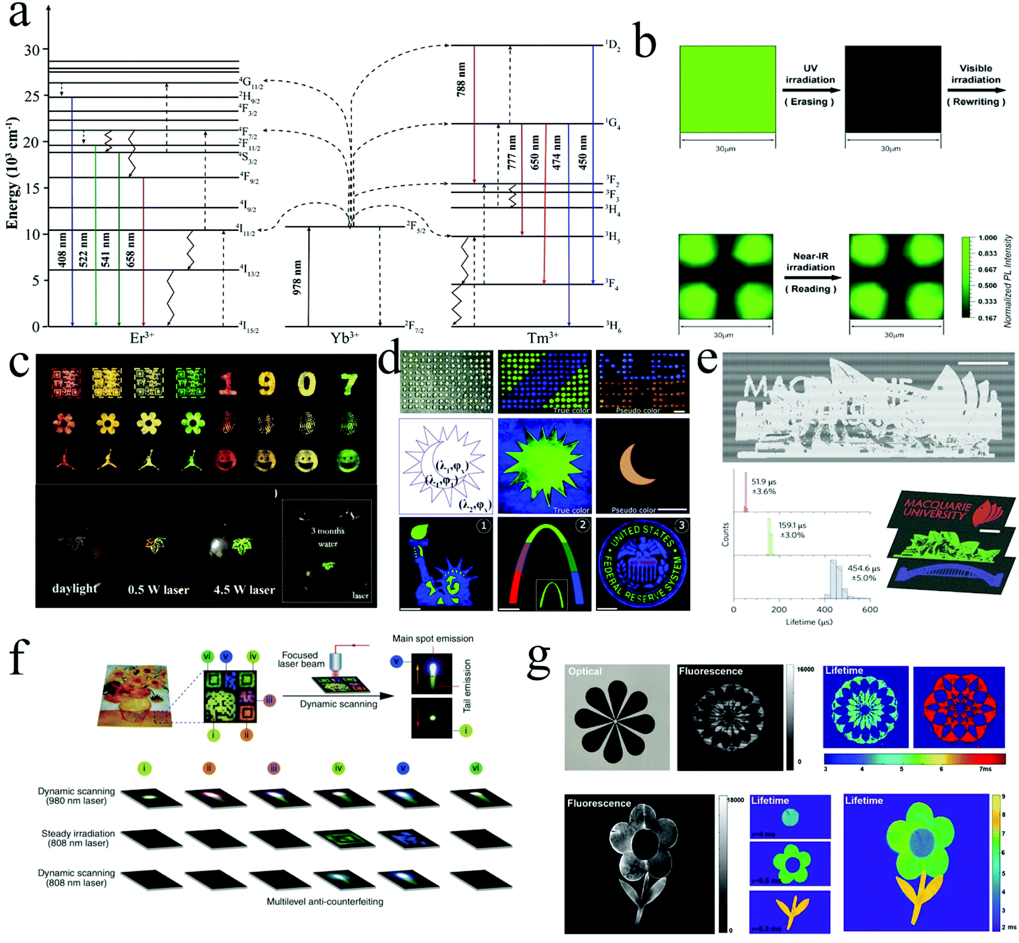 | ||
| Fig. 4 (a) The mechanism of the UCL process of co-doped rare-earth-doped NPs. (b) Demonstration of the reversible writing and erasing process of the composite film under 980 nm excitation for 3600 s. Reproduced with permission.57 Copyright 2011, Wiley-VCH. (c) Multi-level data storage application with Cs3YbF6:Er NCs@glass up-conversion inks. Reproduced with permission.58 Copyright 2020, Elsevier. (d) Demonstration of two-mode multi-level data storage for security purposes realized by luminescence wavelength and phase angle hybrid optical encoding. Reproduced with permission.59 Copyright 2017, Royal Society of Chemistry. (e) Schematic of UCNPs lifetime-encoded multi-level data storage. Reproduced with permission.60 Copyright 2013, Springer Nature. (f) Multi-level data storage application with Mn2+-activated core–shell UCNPs. Reproduced with permission.61 Copyright 2017, Springer Nature. (g) Demonstration of multi-level security data storage based on the fluorescence and lifetime of UCNPs. Reproduced with permission.62 Copyright 2020, American Chemical Society. | ||
In contrast with the emission color optical encoding dimensions mentioned above, a novel encoding dimension for UCNPs was proposed by studying their luminescence kinetics, such as the quick response of the phase angle of UCL to harmonic-wave excitation.59 A double-encryption-concept applying special beads composed of UCNPs and a photo-polymerizable polymer was proposed. The beads encapsulated by the mixture of UCNPs of two different colors (blue and green) and phase angles were arranged to construct a certain-pattern-encrypted rectangular array, as shown in Fig. 4c. Under the decoding operation, when the array was irradiated by a sustained-wave NIR laser, a pattern of blue and green diagonal stripes was obtained. Furthermore, two types of deeply encrypted data encoded with particular phase-angles were recognized by analyzing the phase-angle information. Therefore, the modulation of the phase angles and the diagonal patterns of alternating green and blue beads offered a new way to develop high-capacity and high-security optical data storage. However, most of the optical data storage systems based on polymers show inferior high-power laser resistance ability, which significantly limits their use in high-security data storage.63 To obtain high-stable optical data storage, Wang et al. successfully developed a novel optical data storage medium which was composed of glass embedded with in situ-crystallized Cs3LnF6 (Ln = Y, Yb, Lu, Sc) cubic nanocrystals.58 A series of encoded patterns with UCL properties were assembled by applying glass inks containing the Cs3YbF6:Er nanocrystals and patterning them on a metal sheet by employing the screen printing technique. As demonstrated in Fig. 4d, all the patterns showed obvious changes of up-conversion emitting color on account of laser illumination-induced photo-thermal effects. The glass-stabilized Cs3LnF6 nanocrystals with noticeable photo-thermal effects exhibited remarkable long-term stability under irradiation with increasing laser power from 0.5 W to 4.5 W or exposure to water for 90 days.
Moreover, to further improve the storage capacity of optical data storage, the luminescence decay lifetimes of up-conversion luminescent nanocrystals were gradually developed. Lu et al. reported a novel multiplexing concept based on upconversion nanoparticles (UCNPs) by manipulating the PL decay lifetimes to construct an encoding temporal dimension in a wide range from microseconds to milliseconds.60 By modulating the concentration of the Tm ions in the 40 nm NaYF4:Yb,Tm nanocrystals, the lifetime of the blue-emitting UCNPs could be prolonged from 48 μs (4 mol% Tm) to 668 μs (0.2 mol% Tm). A composite image consisting of three over-lapping pictures was patterned with three different PL lifetimes with Yb![[thin space (1/6-em)]](https://www.rsc.org/images/entities/char_2009.gif) :Tm ratios of 20:4, 20:1, and 20:0.5 (mol%:mol%), as shown in Fig. 4e (top). By applying time-resolved scanning cytometry, a picture with complex images was decoded into three separate images because they possessed three distinct PL lifetimes of 52, 159, and 455 μs, as illustrated in Fig. 4e (bottom). Additionally, only authorized users who knew the accurate decoding regulation of the PL lifetimes could access the encoding data, which provided a new approach to ensure data safety. Furthermore, the regular arrangement of UCNPs into submicrometer-scale and even into nanometer-scale storage units offers a new choice for superhigh-security and high-capacity optical data storage by employing PL lifetimes as bits of digital information.
:Tm ratios of 20:4, 20:1, and 20:0.5 (mol%:mol%), as shown in Fig. 4e (top). By applying time-resolved scanning cytometry, a picture with complex images was decoded into three separate images because they possessed three distinct PL lifetimes of 52, 159, and 455 μs, as illustrated in Fig. 4e (bottom). Additionally, only authorized users who knew the accurate decoding regulation of the PL lifetimes could access the encoding data, which provided a new approach to ensure data safety. Furthermore, the regular arrangement of UCNPs into submicrometer-scale and even into nanometer-scale storage units offers a new choice for superhigh-security and high-capacity optical data storage by employing PL lifetimes as bits of digital information.
Optical data storage based on only one optical characteristic of luminescent materials has a relatively low capacity for data storage and cannot prevent complex counterfeiting. Therefore, there is a push to develop binary temporal up-conversion codes (luminescence color and luminescence lifetime) to greatly improve the capacity of the optical data storage and prevent complex counterfeiting at the same time. Liu et al. successfully developed a particulate platform that integrated the long lifetime of Mn2+ UCL and the relatively short lifetime of lanthanide UCL, allowing the construction of binary-temporal codes for efficient information encoding.61 Additionally, without the use of complex time-gated decoding instrumentation, the as-prepared Mn2+-doped NPs were still able to realize multi-level anti-counterfeiting with a high identification throughput rate. The as-prepared multilayer nanocrystals showed the ability to synchronously emit short and long lifetimes of emissions when excited at either 980 or 808 nm, which provides novel optical materials that are ideal for multi-level authentication to prevent product forgery. 2D hidden patterns on a rewritable artwork were set up by printing Mn2+-doped UCL NPs of different compositions as a proof-of-concept test (Fig. 4f). The smart design for the establishment of binary up-conversion colors with two clear time-scales and the use of a focused laser beam offers a new way to enable high-capacity and high-security optical data storage without the requirement for a time-gated apparatus, which would significantly promote the application of this design in daily life. Although the methods mentioned above show great potential in high-capacity and high-security optical data storage, it is difficult to realize high-order encoding and visualization processes through the scattering layers at the same time. To achieve this, Tan et al. successfully devised a core in combination with a three-shell multi-layer structure of NaYF4:Yb3+/Er3+–NaYbF4–NaYF4–NaYF4:Nd3+, in which the inactive NaYF4 shell was regarded as an energy moderating layer to modulate energy transfer from the outermost light-absorbing layer to the inner-core domain to produce a long lifetime of shortwave infrared PL at 1532 nm. Three overlapped patterns of NPs with different lifetimes were stamped on a flat A4 paper by utilizing home-made temporal-security inks (Fig. 4g top). Moreover, encoding and decoding of the flower pattern utilizing NPs-made security inks with three different PL lifetimes (4, 6.5, and 8.3 ms) revealed the use of the core–multi-shell NPs mentioned above for temporal multi-level anti-counterfeiting, as presented in Fig. 4g (bottom). The optical image, steady-state shortwave infrared luminescence imaging, and temporal optical multiplexing showed that core–multi-shell NPs hold great promise for superhigh-capacity and high-security optical data storage.
Rare-earth-doped up-conversion luminescence nanomaterials (REULNMs) have unique electronic structures, smart multi-shell structure designs, and high density of energy levels; thus, these nanomaterials are suitable for high-resolution information read-out and high-security information storage in optical information storage applications. There are two efficient ways to achieve high-capacity and high-security optical data storage. Firstly, by modulating the doping concentration of the rare-earth element in the REULNMs and smartly designing the core–shell structure of the REULNMs, the lifetimes of the REULNMs can be tunable in a wide range, which can greatly improve the capacity and security of the optical data storage. Secondly, the phase angle-encoded UCL nanocrystals and the binary temporal up-conversion codes of Mn2+-activated nanoparticles offer a new approach to obtain multiplexing applications, which also has the potential to enable high-capacity and high-security optical data storage. Particularly, the luminescence performance of REULNMs can be precisely tuned by exciting them with different kinds of lasers. Moreover, the continuous intermediate energy levels of REULNMs are relatively stable, which enables the data read-out process with low exciting laser power, resulting in low energy consumption for the overall processes. REULNMs embedded in storage mediums with high stability, such as glass and ceramics, can be used to fabricate optical data storage devices with long working lifetimes. The density and capacity of the optical data storage can be highly improved by the fabrication of 3D assemblies of NPs, other film-forming technologies, super-resolution technologies, and time-gated setups. If the REULNMs can be crystallized inside glass or ceramics by utilizing the femtosecond laser-direct writing method, the density of the optical data storage based on REULNMs will be greatly improved. Moreover, the optical data storage with REULNMs embedded in the inorganic medium exhibits higher security and a longer lifetime compared with other optical data storage with REULNMs embedded in organic media.
Optoelectronic data storage
Optoelectronic data storage combining electrical signal storage with optical signal storage shows great potential in emulation of optogenetics-modulated artificial synapses.64–66 Moreover, the integration of memory and computing of optoelectronic data storage can break through the limitation of the classical Von Neuman computer architecture and the restriction of Moore's Law. These benefits of optoelectronic data storage have attracted great interest for its important role in making inroads into high-capacity data storage to address the data explosion of global information. Optoelectronic data storage devices can be categorized into two main types based on their structures: two-terminal memristive devices and three-terminal transistor memories. The recent advances in optoelectronic data storage devices and their applications are concluded as follows:Optoelectronic data storage based on memristive devices
As an important family of memristive devices, resistance random access memory (RRAM) devices have a classical sandwiched form of metal-dielectric-metal consisting of two-terminal electrodes and a thin insulating film (Fig. 5a and b). In an RRAM cell, the electrical conductivity of the thin insulating film can be significantly reversibly modulated to a low-resistance state (LRS), an intermediate-resistance state (IRS), and a high-resistance state (HRS).67,68 The resistance change from the HRS to the LRS is defined as a SET process, while the contrary resistance change is defined as a RESET process, as depicted in Fig. 5c and d. The voltage employed on the device resulting in the realization of the SET process is determined as the SET voltage, and the voltage employed on the device leading to the realization of the RESET process is determined as the RESET voltage. Moreover, the modulated conductance value of the thin film can be stored for a long time.69–74 Therefore, the thin film between the two electrodes is a key factor to decide the function of the RRAM.75–78 The materials with switchable resistance that are applied to fabricate the thin films are the most valuable part for the performance of the RRAM device.79–81 However, the proposed mechanism of the resistance switching (RS) is not only affected by the materials used for the thin film but is also influenced by the selected electrodes and the interface in the heterojunction area constructed by the materials used for the thin film and the electrodes.82,83 LNMs (2D organic–inorganic hybrid perovskites, group III–V, II–VI, and IV–VI QDs, inorganic perovskite QDs, up-conversion luminescence nanomaterials, etc.) have been applied to fabricate thin films by low-temperature, large-scale, and solution spin-coating methods instead of high-temperature, high-vacuum, and high-cost device fabricating approaches.84,85 Additionally, LNMs can exhibit excellent photostability and fast photoelectric response properties even under prolonged irradiation times. Therefore, considering the physical forming mechanism of the conductive channel based on LNMs, the RS mechanism can be mainly classified into three forms, ion-migration, charge-trapping, and redox-reaction, owing to the electrochemical metallization and valence changes across the insulating film of the RRAM device:86–91 (i) the RRAMs based on the ion migration mechanism, also called filament-based resistance devices, can bridge the two electrodes by forming a highly localized and restricted filament between the two electrodes, resulting in a great change of the local resistivity and a high current ratio.92–98 (ii) Under a high bias between the two electrodes, charges are poured into the insulator layer through Fowler–Nordheim tunneling and mostly trapped by the trapping centers in the LNMs or heterojunctions between LNMs and other nanomaterials. Therefore, the RRAMs based on the charge trapping mechanism can change the electrostatic barrier properties of the memristive device by the charge trapping and de-trapping process, which affects the conductance of the thin film. (iii) The RRAMs based on the redox reaction mechanism can induce changing of the electrostatic barrier structure and charge transport of the active materials in the RRAM. As a result, the conductance of the thin film will be modulated by the change in the oxidation–reduction states.99 Considering the resistive switching mechanism of the luminescent nanomaterial-based RRAM device, the photovoltaic effect and photogating effect are the main reasons which explain the changing of the operation current and SET/RESET voltages depending on the wavelength and the intensity of light. A simple review of the various LNM-based memristive devices is summed up in Table 1, and the recent achievements in this field are shown in the following discussions. The LNMs which apply to the fabrication of memristive devices can be sorted into three groups on the basis of their chemical compositions. The first group of LNMs used to fabricate memristor devices is group II–VI, III–V, and IV–VI QDs. The mechanisms of the RRAM devices based on PbS QDs can be categorized into two types: charge-trapping and the formation of a conductive filament. Li et al. developed a fully light-controlled memristor device by utilizing the inorganic PbS/ZnO QDs heterojunction as the dielectric layer and Al/ITO as the electrodes (Fig. 6a).100 Under UV light irradiation, the current increased continuously with increasing sweep time when a negative voltage sweeping across the electrodes was applied, while the current deceased gradually without UV light irradiation. However, under IR light, the current slightly decreased when applying a positive voltage across the two electrodes, and the current gradually increased without IR light irradiation, as depicted in Fig. 6b. As with the emulation of postsynaptic current (PSC), the UV light irradiation exhibited a clear excitatory effect, while the IR light irradiation showed an inhibition effect, as presented in Fig. 6c and d. From the results mentioned above, the mechanism of the inorganic PbS/ZnO QDs heterojunction-based memristor device was that ZnO offered ionized oxygen vacancies with UV light irradiation, while the PbS QDs provided the photogenerated carrier transfer at the interface in the hybrid-heterojunction and indirectly manipulated the ionized oxygen vacancies under IR light irradiation. Therefore, the use of additional light to adjust the conductance of the memristor device offered a new approach to obtain high-density and high-capacity optoelectronic data storage devices. Due to its outstanding optoelectronic performance, the memristor device showed great potential to emulate synaptic plasticity and realize photonic computing and neuromorphic computing. Chen et al. designed a photonic memristive device by depositing a mixture of PbS QDs and PMMA composite materials on a substrate with the Ag electrode on top and the ITO electrode at the bottom, as shown in Fig. 6e.101 As demonstrated in Fig. 6f, the I–V characteristics of the RRAM device showed that the device could easily achieve multi-level data storage by setting different compliance currents. Moreover, with the additional irradiation of UV (405 nm), deep red (808 nm), and IR (1177 nm) light on the device, the set voltage of the memristive device deceased clearly as the light laser power density increased, as illustrated in Fig. 6g, h, and 5i. The supernumerary light was chosen as the additional terminal of the device to highly improve the density and capacity of the information storage. The mechanism of this RRAM device was the formation of Ag conductive filaments that contributed to the RS behavior, which was demonstrated by conductive AFM measurements. However, the core–shell QDs used for the fabrication of the RRAM device showed that the charge trapping and Ag conducting filaments both contributed to the RS behavior. Wang et al. developed a core–shell InP/ZnS QDs-based memristor by depositing the core–shell InP/ZnS QDs on a glass substrate with the bottom ITO electrode and top Ag electrode (Fig. 7a). As demonstrated in Fig. 7b and c, the memristor device exhibited RS mode under dark conditions, while it transferred to threshold switching (TS) with UV light irradiation. Moreover, the memristor device had a lower set voltage with UV light irradiation than without the illumination of UV light. Additionally, the I–t measurements of the memristive device showed that the devices processed higher selectivity and less power consumption via light modulation (Fig. 7d). Subsequently, a multi-level visual data storage system with integration of a 9 × 9 crossbar array was built by the light-triggered RS to TS transition combined with electrical SET operation, as shown in Fig. 7e. Therefore, the memristor device showed great potential in enlarging the memory window and obtaining multiple storage levels to enable high-capacity and high-density optoelectronic data storage with additional light as the extra terminal. Overall, the memristor device was also applied to emulate visual-neuronal behaviors consisting of threshold-spike, strength-modulated-spike frequency properties, and all-or-none spiking. The mechanism of this memristor device involves charge-trapping and Ag conductive filament mechanisms, which was confirmed by the testing results of electrostatic-force microscopy, kelvin-probe-force microscopy, temperature-related resistance, and metallic characteristics of the LRS memristor, respectively. Wang et al. designed another core–shell QDs-based RS device with a device structure of Ag/ZnSe–ZnS/ITO, as shown in Fig. 7f.104 As evidenced in Fig. 7g, the RRAM device exhibited unique bipolar multi-level RS performance under the investigation of the I–V curves. Moreover, multi-level data storage was obtained by various reading voltages, as shown in Fig. 7h. After the different SET and RESET processes, three states of the bipolar I–V curves of the devices were obtained. These results indicated that the formation of the Ag conducting filaments and the trapping holes contributed to the bipolar multi-level RS behavior. Moreover, the unique bipolar multi-level behavior was employed to implement a Markov chain algorithm, creating a true random number generator. Additionally, the device showed multi-level RS behavior under irradiation with different light wavelengths, as presented in Fig. 6i. The competition of the space-charge limited current conducting mechanism and the electrochemical metallization mechanism offered a new approach to develop high-capacity and high-density optoelectronic data storage. Cheng et al. designed a new concept core–shell QDs-based RRAM device with a device structure of ITO/[CdSe/ZnS @PMMA]/Ag, which combined electrochemical metallization memory and random lasers, as shown in Fig. 7j.103 The RRAM device with various sizes of QDs both possessed a high current on–off ratio of 105 with a set voltage of less than 1 V. By modulating the pumping power and selecting different sweep voltages, an AND-gate logic for random-laser-signal feedback was obtained when the device was in the ON-state (Fig. 7k). Furthermore, on account of the quantum size effect, choosing different sizes of QDs resulted in wide-spectral-optical reading, which could offer more digital bits for AND-gate-logic, as depicted in Fig. 7l. The new concept based on the combination of random-lasers in RRAMs offered a remarkable option to obtain optical/electric composite logic, which showed great potential in fabricating ultrahigh-capacity and ultrahigh-density multi-level optoelectronic data storage devices. The proposed mechanism model of the RRAM devices belonging to the Ag conductive filament mechanism. The second group of the LNMs used to fabricate memristor devices is 2D-organic–inorganic hybrid and inorganic halide perovskite nanomaterials. Organic–inorganic halide perovskite nanomaterials are strongly affected by ion migration and have drawn significant attention for their applications in RRAM devices. Zhu et al. designed a memristor device on the basis of CH3NH3PbI3 (MAPbI3) materials with a structure of metal/MAPbI3/Au, as illustrated in Fig. 8a.105 In the RRAM device, RS behavior with relatively low SET and RESET voltages was observed under different negative and positive voltage sweeps, as shown in Fig. 8b. Under a series of different illumination intensities, the SET voltage of the RRAM device slowly increased while the RESET voltage of the device gradually decreased, as depicted in Fig. 8c and d. Light was chosen as an additional stimulus to modulate the annihilation/formation of conduction channels, which highly improved the capacity and density of the MAPbI3-based memristor device. Moreover, Zhu et al. further studied the optogenetics-Inspired tunable synaptic functions of the MAPbI3-based memristor device with a new lateral device structure of Ag/MAPbI3/Ag, as illustrated in Fig. 8e.106 Although the SET process of the memristor device became increasingly difficult with increasing illumination intensity, the RRAM device possessed the ability of multi-level data storage (Fig. 8f). Overall, the conductance of the memristor device could be adjusted by electrical stimulation pulses and different light intensities, leading to the simulation of light-regulated Ca2+ dynamics in biological synapses by optogenetic techniques, as depicted in Fig. 8g–i. The formation and annihilation of Ag or iodine vacancy conductive filaments of the memristor device under the modulation of light irradiation or voltage bias sweeps were studied in detail by the limited spatial resolution of element mapping in EDX tests. The application of organic–inorganic hybrid halide perovskite nanomaterials in fabricating memristor devices not only provides a new approach to develop high-capacity and high-density optoelectronic information storage but also promotes the advancement of future neuromorphic computing applications.113,114 However, unlike organic–inorganic hybrid halide perovskite-based memristor devices, all-inorganic halide perovskite material-based memristor devices can obtain higher stability and performance. Wu et al. designed a memristor device on the basis of all-inorganic halide perovskite CsPbBr3 nanocrystals with the 3D device structure of Ni/ZnO/CsPbBr3/FTO, as evidenced in Fig. 9a.107 The device could realize electric field-induced bipolar RS operations with a high current on–off ratio (>105) and low SET/RESET voltage, which were achieved by ZnO capping on the CsPbBr3 nanocrystal film (Fig. 9b). Moreover, the RRAM device exhibited good stability after long SET/RESET processes, as illustrated in Fig. 9c. Additionally, the device achieved a second resistive state after applying light illumination on the device; therefore, it can be used to fabricate a high-capacity and high-density optoelectronic memory device (Fig. 9d). The mechanism of the RRAM device was affected by the introduction of ZnO, which effectively blocked the channel for ionic migration; thus, the charge trapping mechanism dominated the migration in this RRAM device. Wang et al. designed another RRAM device with high stability and performance based on all-inorganic perovskite CsPbBr3 QDs with a 3D device structure of ITO/PMMA:CsPbBr3/Ag (Fig. 9e).108 As demonstrated in Fig. 9f and 8g, multi-level data storage was achieved in just one memory cell when the compliance current of the device was confined at different levels or the device was irradiated under different light intensities. The mechanism of the device was studied in detail by analyzing the results of the SEM and EDX measurements (Fig. 9h and i). The results of the SEM and EDX measurements indicated that both the Ag metallic conductive filaments and bromide vacancy filaments contributed to realizing the transformation of the resistance state from HRS to LRS in the RRAM device with the Ag-anode.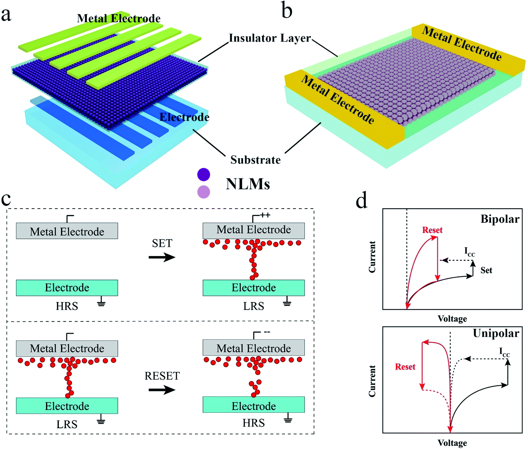 | ||
| Fig. 5 (a) Diagram of the vertical structure of the RRAM device. (b) Diagram of the planar structure of the RRAM device. (c) Diagram of the layout of the conductive filament mechanism of the RRAM device. (d) The two types of typical switching in RRAM (bipolar switching: upper panel, unipolar switching: lower panel). | ||
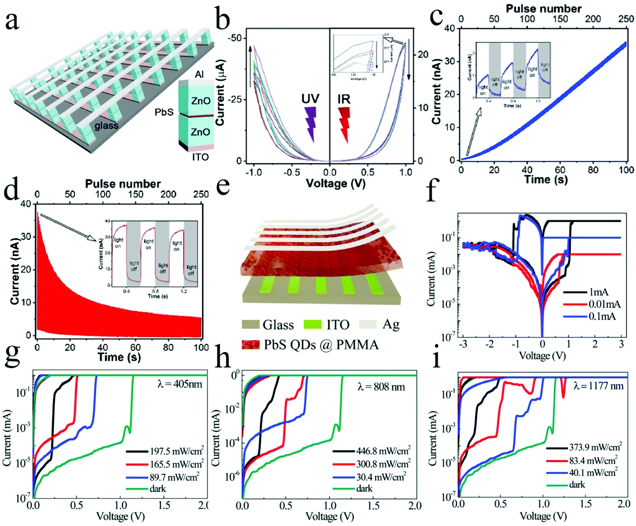 | ||
| Fig. 6 (a) 3D schematic of the inorganic PbS/ZnO heterojunction-based memristor device array. (b) The I–V curves of the memristive device with UV and IR light irradiation. (c–d) The emulation of EPSC plasticity and IPSC plasticity by stimulation with 365 nm light pulses and 980 nm light pulses, respectively (light pulse: duration 0.2 s, interval 0.2 s). Reproduced with permission.100 Copyright 2020, Elsevier. (e) The 3D device structure of the PbS QDs and PMMA composite film-based RRAM device. (f) Typical I–V curves of the RRAM device at various compliance currents. (g–h) Typical I–V curves of the RRAM device in the dark and with irradiation at different wavelengths. Reproduced with permission.101 Copyright 2017, Royal Society of Chemistry. | ||
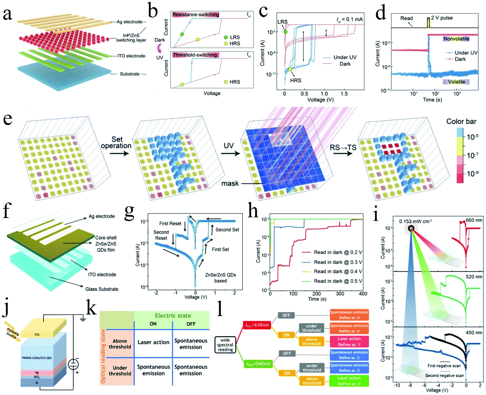 | ||
| Fig. 7 (a) 3D schematic of the InP/ZnS QDs-based RRAM device. (b) The I–V curves of the two switching models of the RRAM device in the SET process in the dark (nonvolatile feature, top) and under UV light illumination (volatile feature, bottom). (c) Comparison of the I–V characteristics in the dark and under UV light irradiation. (d) I–t tests without/with UV light illumination by employing an electrical pulse. (e) Diagram of the multi-level information storage realized in a 9 × 9 integrated crossbar array under the modulation of electrical and optical operation. Reproduced with permission.102 Copyright 2020, Wiley-VCH. (f) Diagram of the RRAM device composed of core–shell ZnSe/ZnS QDs. (g) I–V characteristic of the RRAM device on the basis of ZnSe/ZnS QD with two distinct SET and RESET operations in a sweeping cycle. (h) Multi-level data storage was achieved by various reading voltages. (l) The I–V curves of the RRAM device irradiated with different wavelengths of light. Reproduced with permission.104 Copyright 2020, American Chemical Society. (j) The 3D schematic of the RRAM device on the basis of the core–shell CdSe/ZnS. (k) The defining principle of the random laser signal feedback of the core–shell CdSe/ZnS QDs-based RRAM device. (l) The defining principle of the wide-spectral reading modes with AND-gate-logic. Reproduced with permission.103 Copyright 2020, American Chemical Society. | ||
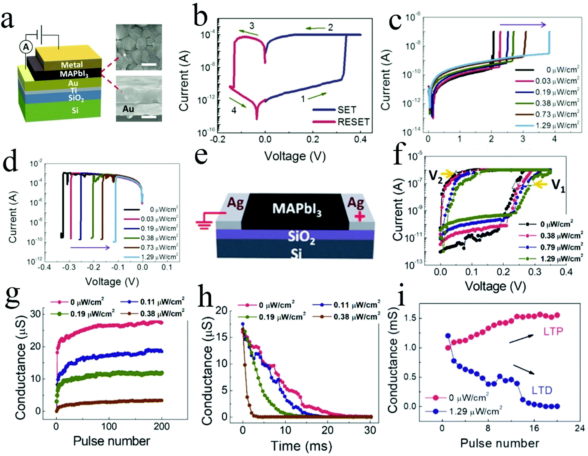 | ||
| Fig. 8 (a) 3D illustration of the MAPbI3-based vertical structure RRAM device. (b) The typical I–V curve of the device during the SET/RESET process (ICC = 10−4 A). The I–V curves of the device under irradiation with various light intensities, (c) during the SET operations, and (d) on the RESET operations. Reproduced with permission.105 Copyright 2018, Wiley-VCH. (e) 3D illustration of the MAPbI3-based planar structure RRAM device. (f) The I–V characteristics of the device under irradiation with various light intensities. (g) Potentiation curves under illumination with various light intensities and in combination with electrical pulses. (h) The I–t measurements of the device under illumination with various light intensities. (i) The formation of STP and LTP in the device under illumination with various light intensities. Reproduced with permission.106 Copyright 2018, American Chemical Society. | ||
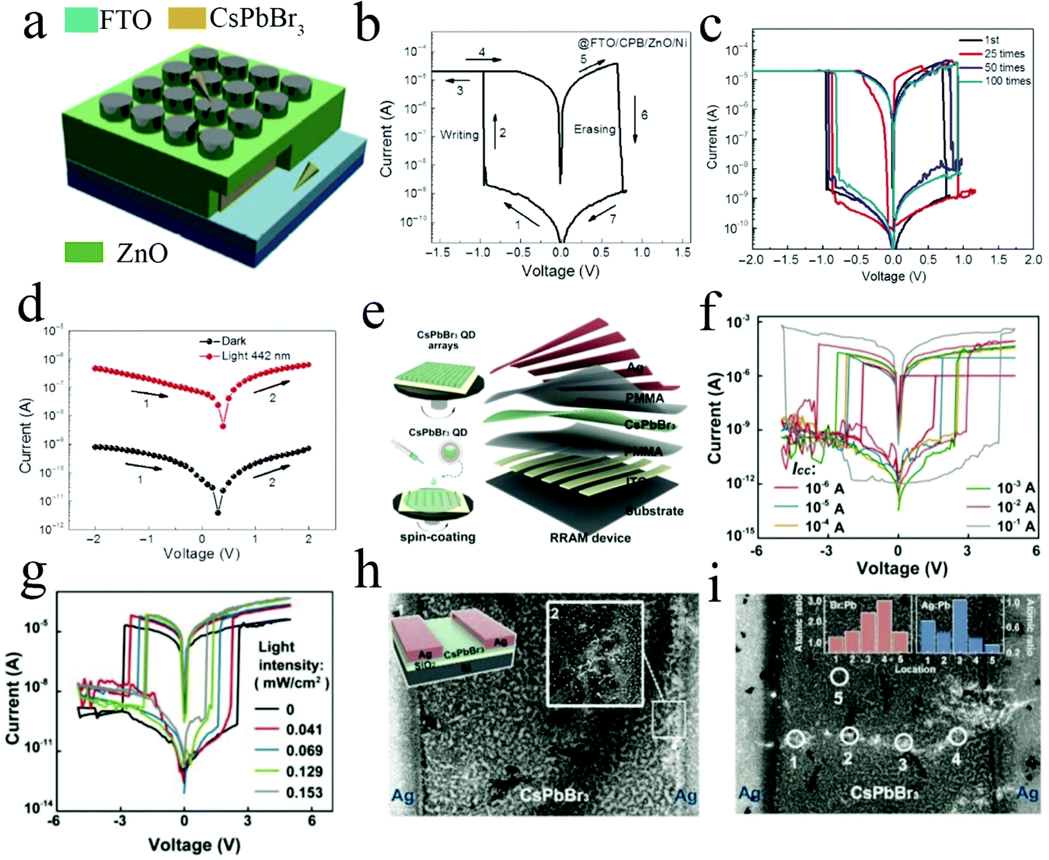 | ||
| Fig. 9 (a) The 3D device structures of the CsPbBr3 NC-based RRAM device. (b) The typical I–V curves of the device. (c) The endurance stability of the device after one to 100 testing cycles. (d) The multi-level data storage realized in the dark and under UV light illumination (1.01 mW cm−2). Reproduced with permission.107 Copyright 2017, Springer. (e) The 3D device structures of the CsPbBr3 QDs-based RRAM device. (f) The typical I–V curves of the device at six different ICC. (g) The I–V characteristics of the device measured in the dark or under different light intensities. (h, i) The formation of the Ag conductive filament in the device as confirmed by the SEM and EDX results. Reproduced with permission.108 Copyright 2018, Wiley-VCH. | ||
| LNMs | Device structure | V set (V) | V reset (V) | ON/OFF ratio | Cycles | Retention time | Ref. |
|---|---|---|---|---|---|---|---|
| PMMA: poly (methyl methacrylate), BP: black phosphorus, QD@NS: QDs + nanosheets, GR: graphene. | |||||||
| PbS QDs | ITO/ZnO/PbS/ZnO/Al | — | — | — | — | — | 100 |
| PbS QDs | Ag/PMMA:PbS/ITO | 1.1 | −1.1 | 104 | — | 104 | 101 |
| InP@ZnS QDs | Ag/InP@ZnS/ITO | 1.45 | −1.1 | 102 | — | 3 × 10⁴ | 102 |
| CdSe/ZnS QDs | Ag/PMMA:CdSe/ZnS/ITO | 1.1 | −1 | 105 | — | 104 | 103 |
| ZnSe/ZnS QDs | Ag/ZnSe/ZnS/ITO | 0.7 | −0.38/−1 | 102 | — | 104 | 104 |
| MAPbI3 | Ag/MAPbI3/Ag | 0.20 ± 0.07 | −0.14 ± 0.08 | 106 | 103 | 104–105 | 105 and 106 |
| Au/MAPbI3/Ag | 0.27 ± 0.10 | −0.15 ± 0.09 | |||||
| Au/MAPbI3/Au | |||||||
| CsPbBr3 QDs | Ni/ZnO/CsPbBr3/FTO | −0.95 | 0.71 | 105 | 100 | 104 | 107 |
| Ag/PMMA:CsPbBr3/ITO | 2.6 | −2.8 | 105 | 5 × 10³ | 4 × 10⁵ | 108 | |
| BP/ZnO QDs | Al/PMMA@BP/ZnO/ITO | — | — | — | — | — | 24 |
| BP/ZnO | Al/BP/ZnO/ITO | 4.48 | −3.26 | 108 | 500 | — | 109 |
| CDs/silk | (Al,Au,Ag)/CDs/silk/ITO | 3.1/—/1 | —/—/−0.9 | 106 | 100 | 106 | 110 |
| UCNPs/MoS2 | ITO/MoS2–UCNPs/Al | 4.6 | −4.4 | 103 | 200 | 104 | 111 |
| QDs/MoS2 | GR/MoS2-QD@NS/GR | 4 | −3.5 | — | 100 | — | 112 |
The last group of LNMs employed to fabricate RRAM devices is black phosphorus QDs,115 carbon dots (CDs), and MoS2 nanosheet composite materials. The memristive devices based on this group of LNMs fully enlarge the application of LNMs with other materials; therefore, the LNMs can be used to fabricate high-capacity and high-density optoelectronic data storage devices.116 Hu et al. developed an RRAM device with a unique assembly of black phosphorus QDs/ZnO (ZB NPs) nano-heterojunctions through a facile colloidal chemistry method; the device exhibited high environmental stability and broadband optical response from UV light to NIR light.109 The device structure of the ZB NPs-based RRAM device is shown in Fig. 10a. As demonstrated in Fig. 10b and c, both the light wavelength and intensity could modulate the conductance of the RRAM device, resulting in the realization of multi-level data storage in the memory cell. Moreover, Ren et al. designed a memristor device based on ZB NPs, as presented in Fig. 10d.24 As the sweeping numbers increased, the conductance of the memristor device was modulated, which resulted in the achievement of multi-level data storage (Fig. 10e). Meanwhile, pulses with different light wavelengths could also adjust the conductance of the memristor device, with the same function as the electric pulse (Fig. 10f). Furthermore, the memristor device composed of ZP NPs showed great potential to emulate essential synaptic functions, and light-controlled plasticity was also evidenced. Although the two memristor devices were made by the same LNMs, the mechanisms of the devices were quite different. The dominant mechanism of the front device was the oxygen vacancy conductive filament mechanism, while the dominant mechanism of the latter device was the charge trapping mechanism. CDs are biocompatible semiconductor nanomaterials with small sizes, excellent optical properties, and low cost of preparation.117 Lv et al. developed photoactive bio-memories based on CD-silk composite materials with the device structure of metal(Al,Au,Ag)/CDs-silk/ITO, as illustrated in Fig. 10g.110 As demonstrated in Fig. 10h, the prepared RRAM device with Ag as the top electrode could not realize the whole SET/RESET processes without light irradiation when the compliance current was set at different levels. However, when the compliance current was set at 1 mA, two SET processes with two low-resistance states and only one RESET process were achieved in the RRAM device irradiated with different light intensities, as depicted in Fig. 10i. These results indicated that the RRAM device with Ag as the top electrode could be used to fabricate multi-level optoelectronic information storage with high capacity and high density when light was introduced into the RRAM device as the extra modulation terminal. Both the charge-trapping process and the Ag conductive filament contributed to the phototunable memory behavior of CDs-silk-based RRAM. 2D layered nanomaterials, including hexagonal boron nitride (h-BN) and semiconducting molybdenum disulfide (MoS2), have attracted great interest in developing optoelectronic devices because of their wide bandgap coverage, particular crystal structures, and facile integration for fabricating optoelectronic and photonic devices.118,119 Zhai et al. developed a NIR optoelectronic RRAM device based on MoS2 nanosheets and a UCNPs heterostructure with a device structure of ITO/MoS2–UCNPs/Al, as depicted in Fig. 11a.111 The heterostructure composed of MoS2 NS and UCNPs served not only as a NIR sensitizer but also as generation/separation centers of excitons, which could expand the light wavelength-sensitive range of the MoS2 NS to the NIR light range. Therefore, high-capacity and high-density multi-level optoelectronic data storage in one memory cell could be easily achieved by the introduction of different NIR light intensities, as shown in Fig. 11b and c. Owing to its multi-level optoelectronic data storage ability, the optoelectronic RRAM device was used to build an optical-assistance storage system which could store the information written by electrical pulses under the assistance of NIR illumination (Fig. 11d). The mechanism of the RRAM device was the charge trapping mechanism, which was elucidated by the results of in situ conductive atomic force microscopy. Afterward, Fu et al. developed another photonic RRAM device based on a MoS2 2D NSs and MoS2 QDs heterostructure with a lateral device structure of GR/MoS2-QD@NS/GR (Fig. 11e). Owing to the photo-induced phase transition in the heterostructure of 2D MoS2 NS and 0D MoS2 QDs, nonvolatile memristors based on the heterojunction demonstrated low power consumption and superhigh density. As shown in Fig. 11f, typical SET/RESET processes were achieved in the RRAM device composed of QDNS with the semiconductor hexagonal phase (2H). However, the phase transition of 2H to metastable metallic tetragonal phase (1T) was realized by laser illumination, which resulted in a higher current ON–OFF ratio (Fig. 11g). Furthermore, as demonstrated in Fig. 11h, the proposed RS mechanism of the RRAM device was investigated in detail by research on the 2H–1T phase transition under low and high voltage sweep processes. Moreover, with increasing density of QDs in the 2D NS and 0D QDs MoS2 heterostructure, the RRAM device could form more extra 1T phases under higher voltage sweep processes; thus, the device exhibited two switching processes, as depicted in Fig. 11i. These results indicated that the 2D NS and 0D QDs MoS2 heterostructure-based RRAM devices are promising for high-capacity and high-density optoelectronic data storage with low power consumption.
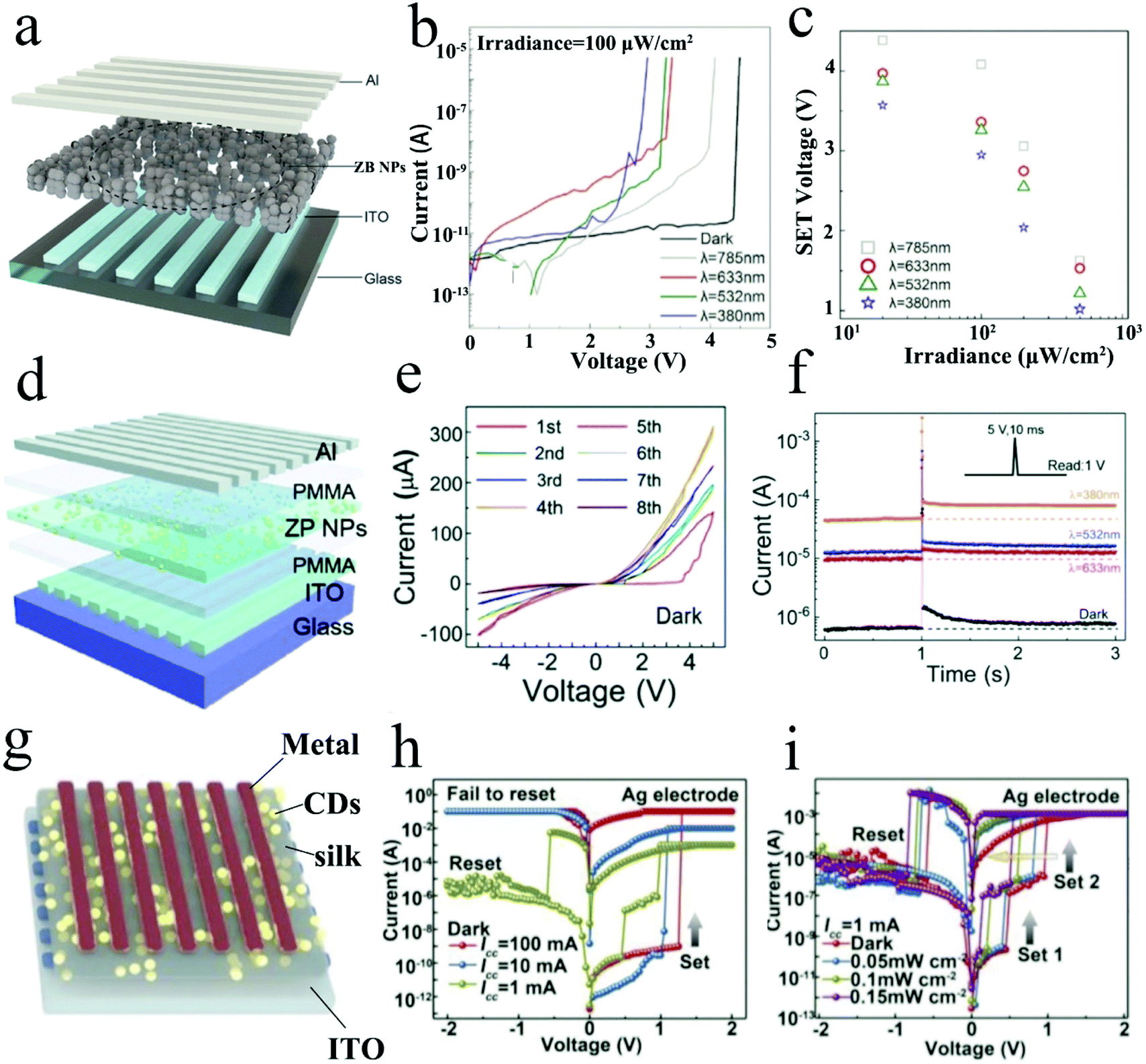 | ||
| Fig. 10 (a) The 3D device structure of a ZB NPs-based RRAM device. (b) The I–V curves of the device at different wavelengths (light intensity: 100 μW cm−2). (c) The SET voltages distributed with variation of the light intensity. Reproduced with permission.109 Copyright 2018, Wiley-VCH. (d) The 3D device structure of the ZP nano-heterojunction-based RRAM device. (e). The typical I–V characteristics of the device under the modulation of voltage in the dark. (f) EPSC characteristics of the device under the modulation of light and electric stimuli. Reproduced with permission.24 Copyright 2018, Royal Society of Chemistry. (g) The 3D device structure of the flexible CDs-silk-based RRAM device. (h) The I–V curves of a CDs-silk-based device at different positive ICC. (i) The I–V curves of a CDs-silk-based device illuminated with various light intensities. Reproduced with permission.110 Copyright 2018, Wiley-VCH. | ||
 | ||
| Fig. 11 (a) Schematic of the 3D device structure of the MoS2–UCNPs-based RRAM device. (b) The typical I–V curves of the device measured upon illumination with different light intensities. (c) Multi-level storage states of RRAM achieved by the irradiation of different light intensities. (d) Schematic of multi-level data storage realized in an integration of the 13 × 13 RRAM array. Reproduced with permission.111 Copyright 2018, Wiley-VCH. (e) Diagram of the 3D device structure of a MoS2 QDNS-based RRAM device. (f, g) The I–V curves of the MoS2 QDNS H1-based device in the dark and under light illumination. (h) The I–V curves from (f) and the formation of filaments of the device. (i) Two-level resistive switching of the MoS2 QDNS-based device in the dark (MoS2 QD ≈ 5.5 × 10⁴ QDs μm−2). Reproduced with permission.112 Copyright 2018, Wiley-VCH. | ||
LNMs, with the features of excellent optoelectrical properties, controllable sizes, high carrier mobilities, and facile synthesis, are suitable to fabricate optoelectronic data storage devices based on RRAM. The combination of light and electric modulation can contribute to the RS of the RRAM device, which enables the realization of multi-level data storage in just one memory cell.120,121 Furthermore, with the development of material design, solution-based method optimization, and bottom-up unconventional processing, exploration of the “one crystal per device” concept has attracted increasing attention. In particular, LNM-based RRAM devices have the potential to emulate optogenetics-tunable synaptic functions and neuromorphic systems, which can further realize the integration of information processing and storage and break through the bottleneck of Von Neumann architecture.122–125 Additionally, light modulation in combination with electric modulation can result in multi-level optoelectronic data storage and lower electricity consumption at the same time. Therefore, the advancement of RRAM devices based on LNMs will greatly promote the development of data storage and alleviate storage shortages and power consumption caused by the data explosion era.
Optoelectronic data storage based on phototransistors
A nonvolatile memory device with a transistor is composed of three electrodes (a bottom-gate electrode and source-drain electrodes), a dielectric layer, and an n-type or p-type semiconductor layer, as illustrated in Fig. 12a. It mainly involves charge trapping flash memory, floating-gate flash memory126–128 (Fig. 12b), and ferroelectric field effect transistor memory,129 in which the information read-out is implemented without any destruction by utilizing drain current (IDS).130,131 Taking a non-volatile memory device with an n-type semiconductor transistor as an example, the main mechanism of the programming/erasing operations of the transistor-based nonvolatile memory device can be divided into three parts: direct tunneling for electrons, Fowler–Nordheim tunneling, and band-to-band tunneling (Fig. 12c). Applying a voltage bias on the gate results in capacitive coupling of the dielectric layer, leading to adjustment of the channel region conductance, and the current across the source and drain, which is bridged by the semiconductor layer, determines the ON and OFF states,132 as depicted in Fig. 12d. Therefore, the interface constructed by the dielectric layer and the semiconductor layer is essentially important for transistor-based nonvolatile memory devices.133–140 To highly improve the performance of the device and even create novel functions, interface-engineering of these heterostructures is presently an active area of research on account of its promising potential for further applications in artificial synaptic, neurorobotic, and photonic in-memory computing.141–145 Generally, the interface within the semiconductor layers consists of traps, grain-boundaries, and other defects, which offer scattering locations for carriers and are harmful to charge transport.146,147 Therefore, modification of the semiconductor layer or the interface between the semiconductor layers and the dielectric layers by incorporation with LNMs will afford thin films with high quality and generate new heterojunctions, thus accelerating the process of charge separating and remarkably improving the optoelectronic performance.148,149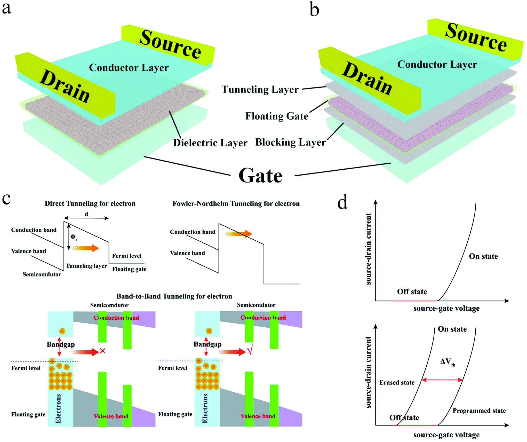 | ||
| Fig. 12 (a) Schematic of an FET-based phototransistor device. (b) Schematic of a floating gate flash memory-based phototransistor device. (c) Three mechanisms of n-type flash memory device operation. (d) Transfer variation curves of the FET-based phototransistor device (top) and the floating gate flash memory-based phototransistor device (bottom). | ||
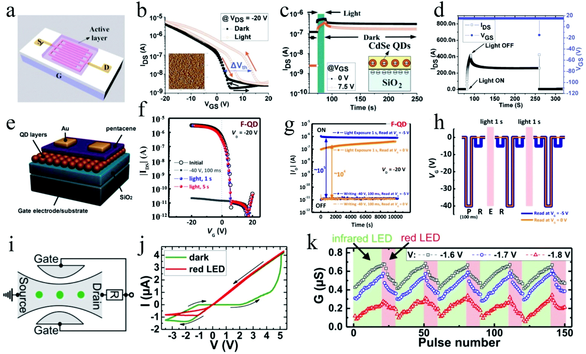
An overview of the advancements in LNM-based phototransistor devices is provided in Table 2, and the recent achievements in this field will be presented in the following three sections. As in RRAM devices, the LNMs used to fabricate phototransistor devices can be categorized into three types. The first group of LNMs used to fabricate transistor devices is group III–V, II–VI, and IV–VI QDs. Chen et al. developed a thin-film phototransistor (TFT) on the basis of poly(3hexylthiophene) (P3HT)/CdSe QDs and investigated its optical responses and memory effects (Fig. 13a).150 As demonstrated in Fig. 13b, TFTs with P3HT/CdSe QDs heterojunctions as the active layer showed higher photo-currents than the corresponding P3HT-only devices, as the addition of CdSe QDs to P3HT created a new interface in the organic semiconductor and then enhanced the separation of excitons. Additionally, compared with the P3HT-only devices, the P3HT/CdSe QDs blend-based TFTs could maintain the metastable state for a long time after light pulse (2.75 mW cm−2, 30 s) irradiation and provide higher ION/IOFF ratios, as shown in Fig. 13c. Moreover, upon illumination with a white light pulse (light on = 80 s, light off = 90 s) and a short pulse with negative gate voltage (100 ms), the drain current was successfully modulated by the light and electrical pulses (Fig. 13d). These results indicated that the P3HT/CdSe QDs-based TFTs could be repeatedly and easily programmed both optically and electrically. The modification of the semiconductor layers by incorporation with CdSe QDs showed potential to achieve optoelectronic data storage. In contrast to the modification of the semiconductor layer, Jeong et al. proposed a strategy to ameliorate the interface built by the semiconductor layer and the dielectric layer by incorporating CdSe QDs capped or surface-modified with small molecular ligands into the interface, leading to efficiently accelerated hole-transport from the QDs to the conducting channel during “photoinduced recovery” and thus realizing a faster erasing process.151 A 3D schematic of the three types of CdSe QD-based phototransistor devices is shown in Fig. 13e. The phototransistor with perfluorinated-thiol-deposited QDs (F-QD) could obtain higher field effect mobility values with more positive turn-on voltages (Von) in comparison with the other two QD-based devices, despite the fact that the pentacene films on F-QD possessed poorer crystallinity and morphology, as depicted in Fig. 13f. Under the modulation of light and electric pulses, the F-QD-based phototransistors exhibited high memory ratios (>105) and maintained a distinct separation between the ON and OFF current states for a long time, as clearly evidenced in Fig. 13g. Under the three programming-reading-erasing-reading (P–R–E–R) cycle operations with the F-QDs-based phototransistor devices, the conductance of the channel could be modulated; therefore, this phototransistor has great potential in high-capacity and high-density optoelectronic optical data storage (Fig. 13h). Maier et al. developed an InAs QDs-based phototransistor with a unique structure in which the InAs QDs connected the GaAs layer and were doped in the AlGaAs layer, as presented in Fig. 13i.155,165 Due to the unique interface ameliorated by the InAs QDs, the phototransistor exhibited a new memristive characteristic, and high conductance was obtained by the positive sweep range operated with red-light irradiation (Fig. 13j). Moreover, by applying different wavelengths of input light onto the phototransistor memory device, the phototransistor memory device could realize infrared-light-writing and red-light-erasing operations (Fig. 13k). The interface-engineering of the GaAs/AlGaAs heterostructure offers a desirable platform for simulation of photonic computing and neuromorphic computing in the future.
 | ||
| Fig. 13 (a) Schematic of the CdSe QDs-based phototransistor device. (b) Transfer variation curves of the phototransistor. (Inset: The AFM testing results of P3HT films with CdSe QDs. Image size is 3 × 3 μm.) (c) The I–t variation curves of the phototransistor device with/without CdSe QDs at different VGS. (Inset: Proposed mechanism.) (d) The I–t variation curves of the phototransistor device under the operations of optical programming and electrical erasing. Reproduced with permission.150 Copyright 2008, American Institute of Physics. (e) The 3D device structure of the CdSe QD film-based phototransistor. (e) Transfer variation curves of the phototransistor with F-QD under voltage or photonic bias. (f) The I–t curves of the phototransistor device with F-QD under voltage or photonic bias. (h) The P–R–E–R process of the phototransistor with F-QD layers realized by the modulation of voltage or photonic bias. Reproduced with permission.151 Copyright 2018, American Chemical Society. (i) Diagram of the phototransistor device and circuit diagram. (j) Memory characteristics of the device in the dark and under red-light irradiation. (k) Programming and erasing operations realized by infrared-light and red-light pulses, respectively. Reproduced with permission.155 Copyright 2016, AIP Publishing. | ||
| Materials | ON/OFF ratio | Memory window (V) | Retention time (s) | Mobility (cm2 V−1 s−1) | Multi-level | Ref. |
|---|---|---|---|---|---|---|
| CdSe QDs | 102 | 5.8 | — | — | 2 | 150 |
| CdSe QDs | 105 | — | 104 | 0.21 | 2 | 151 |
| CdSe/ZnS QDs | — | 3.3 | 104 | 0.21 | 6 | 152 |
| CdSe/ZnS QDs | 6.9 × 10⁴ | 68.5 | 104 | — | 2 | 153 |
| CdSe/ZnS QDs | 104 | 18 | 0.161 | 2 | 154 | |
| InAs QDs | 103 | 6.2 | — | — | 2 | 155 |
| CsPbBr3 QDs | 1.86 × 10⁵ | 16.47 | 103 | 0.24 | 6 | 156 |
| CsPbBr3 QDs | 104 | 42 | 2 × 10⁵ | — | 6 | 157 |
| CsPbBr3 QDs | — | 66.5 | 108 | — | 8 | 158 |
| CsPbBr3 QDs | — | — | — | — | — | 159 |
| CsPbBr3 QDs | — | — | — | — | — | 160 |
| Graphene QDs | 106 | 25.5 | 200 | 1.25 × 10⁻⁴ | 2 | 161 |
| Carbon QDs | 104 | 15.2 | 7 × 10⁶ | — | 6 | 162 |
| NaYF4:Yb/Er | 103 | 10.2 | 105 | — | 3 | 163 |
| NaYF4:Yb/Er–MoS2 | — | — | 106 | 0.381 | 5 | 164 |
Compared with single structure group III–V, II–VI, and IV–VI QDs, QDs with core–shell structures exhibit better optical and electrical properties and show great potential in preparing high-performance phototransistors for light-responsive memory. Han et al. developed UV light-controlled photonic non-volatile memory by adding a spin-coated monolayer composed of core–shell CdSe/ZnS QDs under the tunneling dielectric layers, as depicted in Fig. 14a.152 The phototransistors composed of both n-type and p-type organic semiconductors exhibited 5 levels of data storage under the programming and erasing operations by applying electrical pulses (−8 V/+8 V, duration: 1 s), with or without UV light irradiation, as evidenced in Fig. 14b and c. Moreover, an integrated circuit in combination with the p-channel and n-channel phototransistors was fabricated to verify the feasibility of the two high-performance flexible photonic nonvolatile memories. As shown in Fig. 14d, the transfer characteristics of the integrated circuits exhibited double electrical programming processes and optical erasing processes. These results indicated that the phototransistor devices can be used to fabricate high-performance data storage devices. Wu et al. designed a similar phototransistor device by applying the same CdSe/ZnS QDs as light-responsive floating-gates, as illustrated in Fig. 14e.153 Owing to the modulation of the interface between the blocking and tunneling layers by the CdSe/ZnS QDs, the phototransistor device with nano-channels could obtain an ultra-wide and enhanced memory window (73 V) and six different data storage levels along with high light responsivity and sensitivity under low light power. As demonstrated in Fig. 14f, under irradiation of a series of lights with various wavelengths ranging from UV light to NIR light, light-assisted program processes were successfully achieved. Moreover, the excellent light-responsive properties made it possible to build a programmable optical logic-gate to realize reconfigurable ‘AND’ and ‘OR’ operations on the basis of just one phototransistor memory device by utilizing two light-beams to control the states (Fig. 14g and h). The smart design of the phototransistor device endowed the memory device with the ability to process and recognize images with low power consumption and achieve the function of excellent multi-level data storage. However, Yang et al. developed a phototransistor memory device by spin-coating 6,13-bis(triisopropylsilylethynyl) pentacene (TIPS-pentacene) and core–shell CdSe/ZnS QDs composite materials on a Si substrate as a semiconductor layer (Fig. 14i).154 The uniform mixing of the TIPS-pentacene and the QDs enabled the semiconductor composite layer to obtain high carrier mobility. The semiconductor composite layer with the broadband absorption property of QDs could help the phototransistor device realize a light-responsive program process. As demonstrated in Fig. 14j and k, the phototransistor could achieve optical programming and electrical erasing under the adjustment of different gate voltages and illumination with various light intensities. The memory characteristics of the device showed that the device had great potential in fabricating high-capacity and high-density optoelectronic data storage devices.
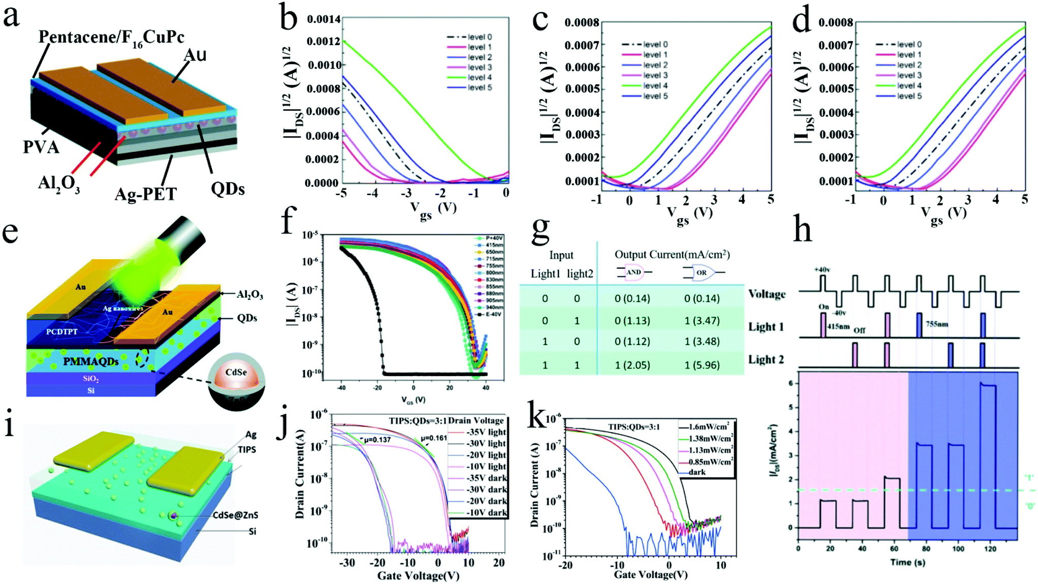 | ||
| Fig. 14 (a) The 3D diagram of the core–shell CdSe/ZnS QDs-based phototransistor. The multi-level optoelectrical transfer variation curves of the (b) p-channel and (c) n-channel phototransistor devices. (d) The I–V variation curves of the inverters after optical programming and electrical erasing. Reproduced with permission.152 Copyright 2015, Royal Society of Chemistry. (e) 3D schematic of the core–shell CdSe/ZnS QDs-based phototransistor. (f) Transfer variation curves of the device under illumination with different wavelengths of light. (g) The ‘AND’ and ‘OR’ logic-gate achieved after optical programming and electrical erasing. (h) Definition standards of the ‘AND’ and ‘OR’ logic gate. Reproduced with permission.153 Copyright 2019, Royal Society of Chemistry. (i) 3D diagram of the core–shell CdSe/ZnS QDs-based phototransistor. (j) Transfer variation curves of the device at various VGS in the dark and under UV light irradiation. (k) Transfer variation curves of the device in the dark and under different light intensities at VGS = −35 V. Reproduced with permission.154 Copyright 2020, Elsevier. | ||
The second group of LNMs used to fabricate phototransistor memory devices is all-inorganic perovskite QDs. Wang et al. developed photonic flash memory by spin-coating CsPbBr3 QDs on the dielectric layer and below the tunneling layer (Fig. 15a). Owing to the charge trapping centers of the CsPbBr3 QDs, the phototransistor-based memory device could realize optical programming and electrical erasing processes under a light pulse (λex = 365 nm, 0.153 mW cm−2, width: 30 s) and an electrical pulse (height: −50 V, width: 1 s), respectively (Fig. 15b). Under a series of different intensities of light illumination, the I–V curves continuously moved toward the positive direction, indicating that the phototransistor memory device could realize multi-level data storage by light pulses (Fig. 15c). Moreover, the phototransistor memory device mimicked neuroplasticity, which results in transformation of the memory retention from short-term memory (STM) to long-term memory (LTM) in the plasticity of the brain, by cumulative modulation with different intensities of light pulses, as demonstrated in Fig. 15d and e. Therefore, the phototransistor memory device based on CsPbBr3 QDs offered an ideal platform to achieve multi-level optoelectronic data storage as well as the integration of data processing and storage. Then, Gong et al. developed another CsPbBr3 QDs-based phototransistor memory device by replacing PMMA with Al2O3 as the tunneling layer, as shown in Fig. 15f.160 Due to the trapped holes generated from the modified interface of the CsPbBr3 layer and Al2O3 layer, the conductance decreased under both the positive and negative gate-voltage sweeping operations (Fig. 15g). After prolonging the illumination time and increasing the light intensity, a remarkable increase of the peak-current values was obtained under both the positive and negative gate-voltage sweeping operations (Fig. 15h and i). Moreover, as depicted in Fig. 15j, the phototransistor memory device showed the ability to mimic neuroplasticity by a paired light pulse-induced PPF test, with a result of effectively firing the EPSC to enhance the STM. As a result, the CsPbBr3 QDs-based phototransistor memory device could be used to fabricate optoelectronic data storage devices and build neuromorphic systems for in-memory computing. To better understand the light-stimulated synaptic plasticity mechanism, Wang et al. developed another CsPbBr3 QDs-based phototransistor memory device that could respond to optical signals as a neuron or a synapse does. As shown in Fig. 15k, the organic semiconductor layer was modified by mixing the CsPbBr3 QDs as the trapping center into the poly(3,3-didodecylquarterthiophene) (PQT-12), which endowed the memory device with the ability to respond to light stimulation. Owing to the charge trapping by the CsPbBr3 QDs, the charge trapped in the QDs could easily realize the de-trapping process with light-assistance. Therefore, the transient photo-response behavior of the phototransistor memory device was observed under irradiation with a series of monochromatic light pulses, as presented in Fig. 15l. A similar series of typical ESPC tests were carried out by single light stimulation to verify that the ESPC values could be efficiently adjusted by the width of the light-pulse, the light intensity, and the number of light-pulses (Fig. 15m). The results of the 30 continuous light stimulation ESPC tests exhibited that the increase in EPSC values and the presynaptic spike-frequency had a near-linear correlation, which confirmed that the light-pulse-stimulated artificial synapse could serve as a dynamic high-pass filter to transmit information (Fig. 15n and o). Moreover, the STM and LTM behaviors of the phototransistor memory device could achieve efficient modification by changing the width of the light-pulse, the light intensity, and the number of light-pulses. Above all, the phototransistor memory device comprising CsPbBr3 QDs could realize the emulation of light-stimulated artificial synapses and can be used to develop photonic neuromorphic devices.
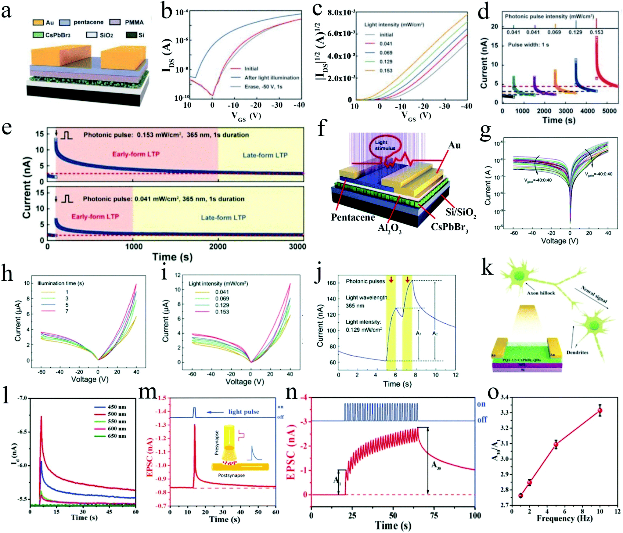 | ||
| Fig. 15 (a) 3D diagram of the CsPbBr3 QDs-based phototransistor. (b) Transfer variation curves of the device in the dark and under UV light irradiation (VDS = −30 V). (c) Transfer variation curves of the device under the irradiation of different light intensities (λex = 365 nm). (d) EPSCs of the device realized by illumination with different light intensities. (e) The LTP of the device was achieved by irradiation with different light intensities. Reproduced with permission.156 Copyright 2018, Wiley-VCH. (f) The 3D diagram of the CsPbBr3 QDs-based phototransistor. (g) Transfer variation curves of the device recorded at different VGS. (h, i) Transfer variation curves of the device operating under different irradiation times and various light intensities. (j) The I–t curves of the phototransistor device triggered by a couple of light pulses. Reproduced with permission.160 Copyright 2020, Royal Society of Chemistry. (k) 3D schematic of the CsPbBr3 QDs/PQT-12-based hybrid-synaptic phototransistor. (l) Transfer variation curves of the device under various wavelengths of light. (m) EPSC of the device achieved by the modulation of light and electric pulses. (n) EPSC of the device triggered by 30 presynaptic optical pulses. (o) Error bars of the phototransistor achieved by five independent measurements. Reproduced with permission.159 Copyright 2019, Wiley-VCH. | ||
In order to develop a high-performance phototransistor memory device, Yang et al. ingeniously designed an organic field effect transistor (OFET) photonic memory device with a vertical structure by adding Ag nanowires to the dielectric layer to connect one electrode and the semiconductor layer, as illustrated in Fig. 16a.158 Additionally, the semiconductor layer composed of organic semiconductor materials and CsPbBr3 QDs successfully created a new interface in the semiconductor layer, which increased the sensitivity of the phototransistor memory device to light stimulation. The conductance of the vertical channel was modulated by a series of light pulses with different light intensities, as evidenced in Fig. 16b. A phototransistor memory device with multi-level data storage was successfully obtained using various intensities of light irradiation under sequential light-assisted programming-reading and electric-assisted erasing-reading (P–R–E–R) operations (Fig. 16c). Meanwhile, remarkable switching properties and endurance characteristics of the phototransistor memory device were obtained under dynamic P–R–E–R cycle operations (Fig. 16d). Owing to the smart design of the vertical phototransistor structure, the IDS showed an abrupt increase and a slight decrease, then maintained a metastable state for a long time when the device was under light pulse illumination (Fig. 16e). Data processing of various systems on the basis of different multi-level phototransistor memory devices was successfully carried out by adjusting the light intensities of the light-assisted programming processes, as shown in Fig. 16f. These results showed that the novel phototransistor memory device had the potential to enable high-capacity and high-density optoelectronic data storage. In contrast to the vertical phototransistor reviewed above, Yang et al. developed another vertical phototransistor memory device based on CsPbBr3 QDs, in which Ag nanowires connected one electrode (source or drain) and the interface constructed by the QDs layer and the organic semiconductor layer, as depicted in Fig. 16g. The unique device structure of the phototransistor memory device greatly modified the interfaces of the semiconductor layer and effectively restrained the “trapped carriers effect” and “interface effect”. Therefore, higher-performance optical programming and electrical erasing processes were observed in comparison with the electrical programming and erasing processes, as shown in Fig. 16h. Moreover, a multi-level data storage process was achieved by adjusting the light pulses with various light intensities, as evidenced in Fig. 16i and j. An array with 10 × 10 device configuration was set up to realize light pulse programming processes and record the light information, verifying the device system integration, imaging, and memory capability (Fig. 16k).
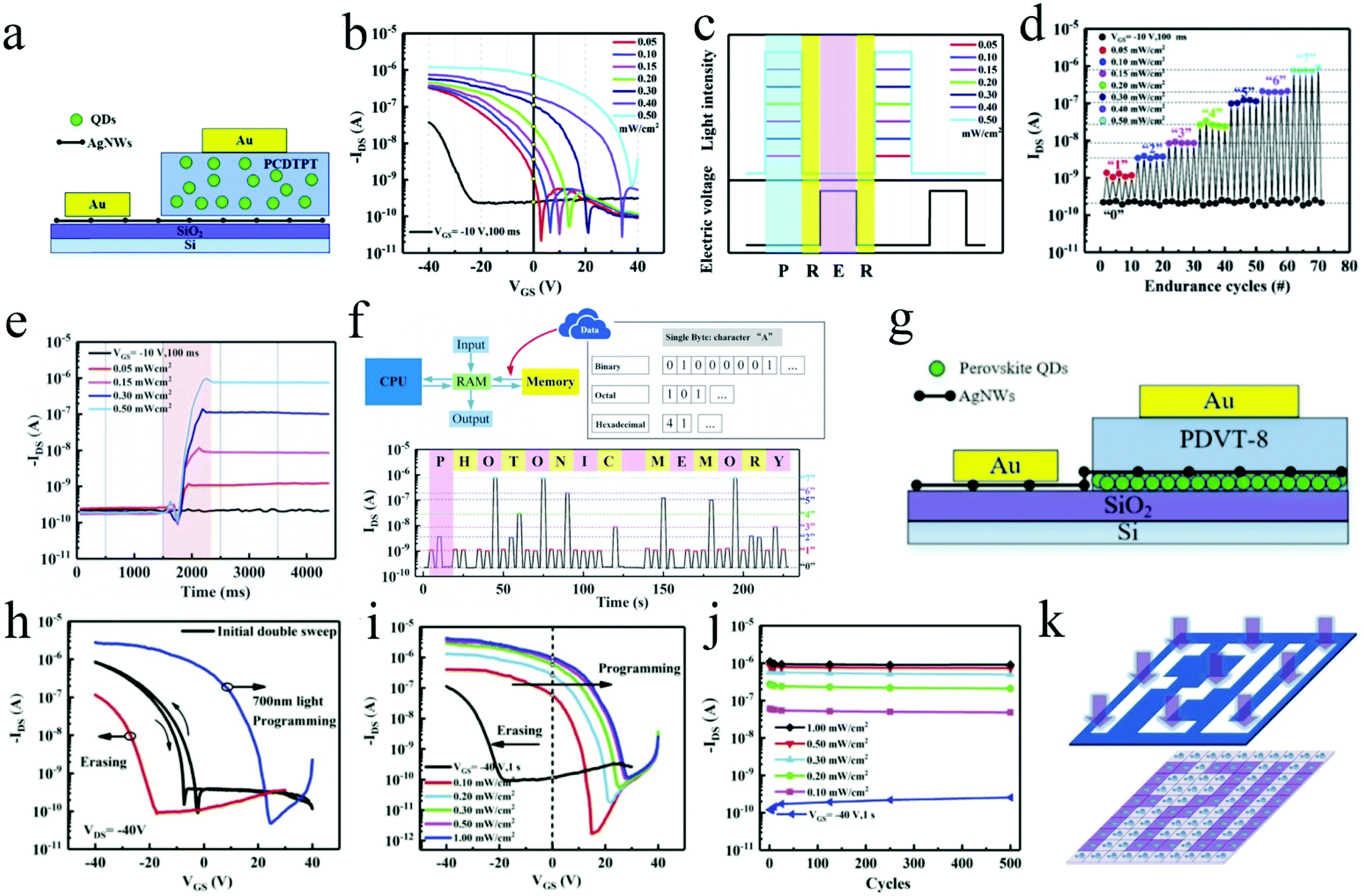 | ||
| Fig. 16 (a) 3D diagram of the CsPbBr3 QDs-based phototransistor. (b) Memory characteristics of the device under UV light (λex = 300 nm, 0.5 s) with various light intensities. (c) The P–R–E–R processes realized under illumination with different light intensities. (d) Multi-level storage states of the device achieved by irradiation with different light intensities. (e) The I–t curves of the device under various light intensities (λex = 300 nm). (f) Definition principles of data processing realized by various systems based on different multi-level optoelectronic data storage processes; the I–t characteristics of the device simulating the data storage process. Reproduced with permission.158 Copyright 2020, Royal Society of Chemistry. (g) 3D diagram of the CsPbBr3 QDs-based phototransistor. (h) Transfer variation curves of the device in the dark and after optical programming and electrical erasing. (i) Memory characteristics of the device achieved by irradiation with different light intensities (λex = 300 nm). (j) The I–t curves of the device under different light intensities (λex = 300 nm). (k) Schematic of the multi-level optoelectronic data storage realized in an integration of the 10 × 10 RRAM array. Reproduced with permission.157 Copyright 2018, Wiley-VCH. | ||
The last group of LNMs used to fabricate phototransistor memory devices consists of UCNPs, graphene QDs, carbon QDs, etc. Conventional flash memory devices are only voltage-driven; thus, it is quite difficult to develop safe and confidential data storage. To address this issue, Zhou et al. designed a novel phototransistor memory device by mixing UCNPs into an organic semiconducting polymer, as depicted in Fig. 17a.163 The addition of UCNPs to the organic semiconducting polymer not only created a new interface in the semiconductor layer but also endowed the organic semiconductor layer with the ability to respond to NIR light. Therefore, the ON states of the phototransistor memory device were successfully achieved by the NIR light programming process (Fig. 17b). As depicted in Fig. 17c, a multi-level data storage process was also obtained by the NIR light-assisted programming operations. Under the sequential P–R–E–R processes, the phototransistor memory device showed excellent endurance characteristics and data retention properties, as evidenced in Fig. 17d and e. Following the achievement mentioned above, Zhai et al. developed another phototransistor memory device by incorporating the heterojunction of the UCNPs and MoS2 nanosheets into the interface built by the dielectric layer and the organic semiconductor layer; this also endowed the device with sensitivity to NIR light stimulation, as shown in Fig. 17f.164 Owing to the UCNPs and MoS2 nanosheets heterojunction acting as the trapping center, the conductance of the channel could be adjusted by the optical programming and electrical erasing processes, as depicted in Fig. 17g. Moreover, when excited by light pulses with different programming times of exposure NIR light and different NIR light intensities, the phototransistor memory device exhibited obvious multi-level optoelectronic data storage (Fig. 17h and i). Under a sequential P–R–E–R test with the same NIR light intensity and different gate pulses, the phototransistor memory device showed excellent endurance characteristics (Fig. 17j). Finally, a demonstration of the artificial neuromorphic computing in the phototransistor was carried out using a single-layered perceptron (SLP) neuromorphic network composed of 784 input neurons and 10 output neurons, as demonstrated in Fig. 17k. Additionally, recognition of the mapping images was successfully achieved through training 15000 times by a single-layer perception-based artificial neuron network, as shown in Fig. 17l. These results indicated that adding LNMs to the phototransistor device not only made it possible to fabricate high-density memory devices but also offered an ideal platform to develop novel up-conversion optogenetics-mediated synapse-like devices for photonic neuromorphic computing.166
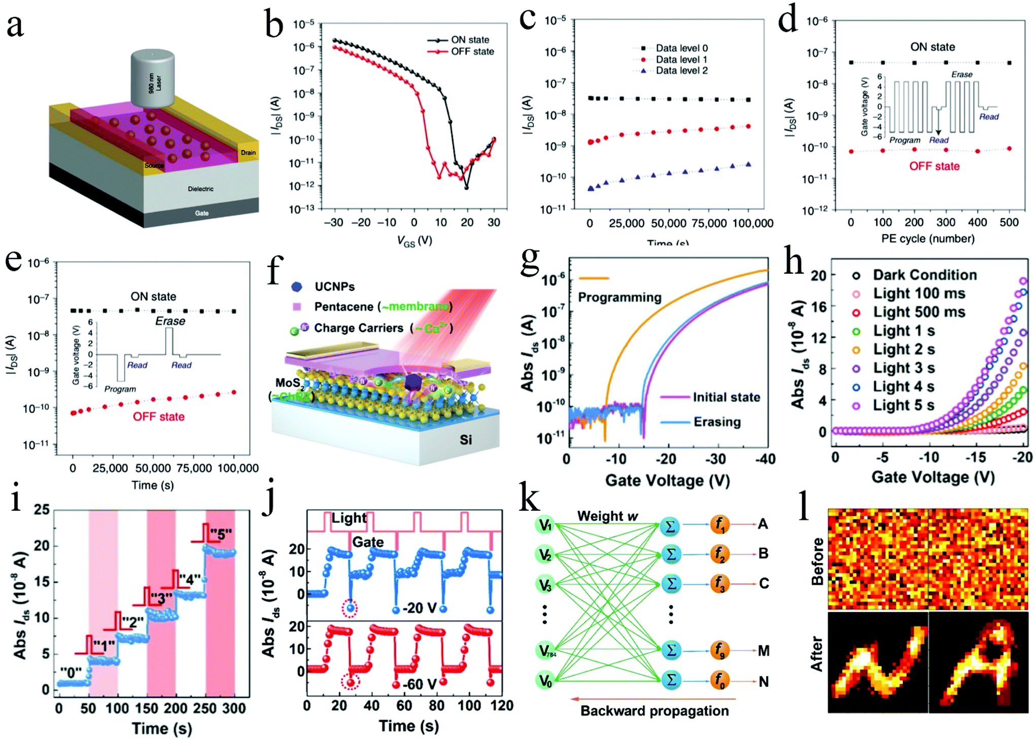 | ||
| Fig. 17 (a) The 3D diagram of the UCNPs-based phototransistor. (b) Transfer variation curves of the device with the assistance of 980 nm laser programming. (c) Transfer variation curves of the multi-level optoelectronic data storage device obtained with the assistance of 980 nm laser irradiation. (d) Endurance properties of the memory device obtained through the P–E cycle operation. (e) Transfer variation curves of the device under the P–E cycle operation. Reproduced with permission.163 Copyright 2014, Springer Nature. (f) The 3D device structure of the MoS2–UCNP-based phototransistor synapse device. (g) Transfer variation curves of the device achieved by the optical programming and electrical erasing operations. (h) Transfer variation curves of the device with various illumination times. (i) Multi-level optoelectronic data storage realized by the illumination of various light intensities. (j) Transfer variation curves of the memory device after optical programming and electrical erasing. (k) Definition principles of the single-layered neuromorphic network. (l) The results of the recognition of letters by the single-layered neuromorphic network through training 15000 times. Reproduced with permission.164 Copyright 2020, Elsevier. | ||
Carbon nanomaterials, including graphene QDs and carbon QDs, possess size-dependent optical and electrical properties and show great potential in fabricating light-sensitive phototransistor memory devices. Kim et al. developed photovoltaic and photoelectric memory based on graphene QDs, as depicted in Fig. 18a.161 The graphene QDs acted as the charge trapping center and assigned a better light-sensitive function to the heterojunction when added to the interface between the dielectric layer and organic semiconductor layer. Therefore, the conductance of the phototransistor memory device could be modulated by 650 nm laser light and the gate bias voltage, as presented in Fig. 18b. These results showed that the graphene QDs-based phototransistor memory device possessed the ability to realize multi-level optoelectronic data storage. According to the study of the carbon nanomaterials mentioned above, Lv et al. lucubrated the neuroplasticity of a carbon QDs-based phototransistor memory device by optical and electrical dual mode modulation. The addition of environmentally friendly CDs/silk composite materials to the interface constructed by the dielectric layer and the organic semiconductor layer created two new interfaces to act as trapping centers and assigned excellent UV light-responsive function to the heterojunction, as shown in Fig. 18c.162 On account of the outstanding optical and electrical characteristics of the CDs/silk composite materials, the phototransistor memory device successfully achieved a light-assisted programming process and electric-assisted erasing process by UV light and a −50 V gate bias voltage, respectively (Fig. 18d). Furthermore, multi-level data storage operations of the phototransistor memory device were carried out using different UV light intensities and UV light programming times, as depicted in Fig. 18e and f. Moreover, LTP and STP of the device were realized by irradiation with different UV light intensities and UV light programming times, as shown in Fig. 18g and h. Finally, a simulation of the artificial neuromorphic computing in the phototransistor was implemented by an SLP neuromorphic network composed of 785 input neurons and 10 output neurons, as demonstrated in Fig. 18i. Additionally, the reliability of the pattern recognition was verified by both “A” and “I” input pattern recognition processes (Fig. 18j). In consideration of the results obtained above, phototransistor memory devices based on composite materials composed of carbon and biomaterials offer a promising way to develop photonic neuromorphic computing.
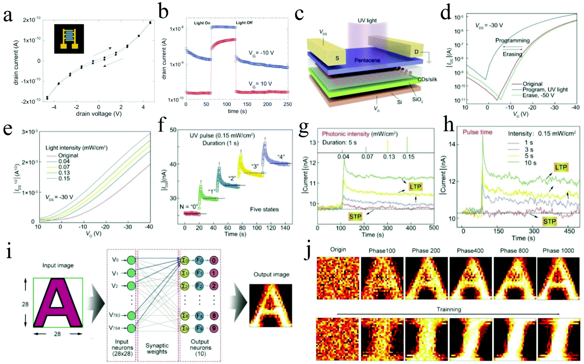 | ||
| Fig. 18 (a) Transfer variation curves of a GQD film-based phototransistor device. (b) The I–t curves of the multi-level optoelectronic data storage device were obtained with the assistance of 650 nm laser irradiation. Reproduced with permission.161 Copyright 2017, IOP Publishing Ltd. (c) The 3D device structure of the CDs/silk-based phototransistor device. (d) Transfer variation curves of the memory device were achieved after optical programming and electrical erasing. (e) Multi-level optoelectronic data storage was realized by irradiation with various light intensities. (f) Multi-level storage states of RRAM achieved by the illumination of various wavelengths of light. (g–h) STP or LTP formation in the device was achieved by various light intensities and different illumination times. (i) Definition principles of the SLP network. (j) The results of the recognition of letters by the SLP network with the evolving training phases. Reproduced with permission.162 Copyright 2019, Wiley-VCH. | ||
The interface-engineering of the heterojunction in the transistor can greatly promote the performance of the device and even construct novel functionalities.167–172 LNMs, with their remarkable optical and electrical properties, are ideal choices to modify the heterojunction of a device and endow it with better UV light, visible light, or NIR light-responsive functions. Compared with traditional transistors, the considerable variety of advantages of LNMs-based phototransistors include low cost, solution processability, and large-area fabrication.173,174 Additionally, due to the remarkable optical characteristics of the LNMs, LNMs-based phototransistors obtain an extra terminal to adjust the conductance of the channel area and thus realize high-capacity and high-density optoelectronic data storage. Moreover, LNMs-based phototransistors can provide an ideal platform to emulate photonic computing and neuromorphic computing, in which storing and processing data can be achieved optically at the same time with large band-width and high-speed.20,175–178
Conclusions
In this review, we have overviewed the latest achievements in nanomaterials technology towards the development of novel optical and optoelectronic data storage systems. The remarkable characteristics of the three types of luminescent nanomaterials (DCLMs, LPLMs, and UCNPs) have been highlighted in their applications in optical and optoelectronic data storage. As with optical data storage, three types of luminescent nanomaterials have been used to fabricate high-capacity and high-density multi-level data storage. On account of the latest achievements in optical data storage, photostimulated luminescence-based optical data storage may be the ideal option to develop high-density and high-capacity optical data storage devices. However, only DCLMs and UCNPs have been used to prepare multi-level optoelectronic memory, while LPLM-based phototransistor memory devices have not been reported. Moreover, the fast-paced development of nanotechnology, STED nanoscopy, and femtosecond laser direct writing are greatly promoting the realization of superhigh-capacity and superhigh-density glass or ceramic-based low power optical data storage with long lifetime and safety. Limited by its single information storage and read mode, optical data storage is only used for long-term and safe information storage. In comparison with optical data storage, optoelectronic data storage can be modulated by optical and electrical signals, which can be used for safe information storage and photonic neuromorphic computing at the same time. However, the reported LNMs-based optoelectronic data storage devices are usually prepared with organic semiconducting materials, which may not realize long lifetimes of information storage. The data storage capacity and data read-write speed of optical and optoelectrical data storage are important characteristics for evaluating data storage systems. In view of the advanced fabrication technology and read-write method employed in optical data storage, optical data storage, which has potential to achieve higher capacity and read-write speeds, is more advantageous.An especially promising prospect for future optical data storage is the advancement of LNM-based glass or ceramic optical data storage. The improvement of methods to fabricate high-performance LNMs in glass or ceramics and the development of STED nanoscopy performance will offer the potential for low-power superhigh-resolution information read-out and data storage with ultra-high capacity and density (every single nanoparticle can be employed as one bit of digital data). Moreover, superhigh-resolution write-in and read-out on the basis of cooperation with two or more LNMs will offer a fully optical solution and a wider lifetime range of temporal coding dimensions for high-security data storage applications. As with optoelectronic data storage, more effort should be made to overcome the current limitations. First, the spin-coating methods used to fabricate optoelectrical memory devices should be modified or even replaced by other advanced methods. The self-assembly of NCs and inkjet-printing technology are two ways to fabricate compact and uniform films which can efficiently reduce the grain boundaries and defects in the thin LNM films fabricated through the spin-coating method.179–181 Secondly, applying stable 2D layered materials to replace organic semiconducting materials as the semiconductor layer will help improve the stability of phototransistor memory devices.182 The heterojunctions constructed by the LNMs and 2D layered materials should be modified by improving the ability to form uniform LNMs films, resulting in better surface bonding, lower initiative trap density, and less non-radiative trap recombination. In addition, a survey of photonic memory devices based on LPLMs should be performed to develop novel high-performance photonic computing memory devices. Second, comprehensive study of photonic memory devices based on LNMs is still necessary for improving the optoelectrical performance of the devices, including their switching speed, device diversification, physical resistance, chemical stability, and expandability toward commercial applications. Third, as with neuromorphic applications,143,183 LNM-based photonic memory devices can achieve superior weight updating regulations by the optical or electrical modulation of their weights, leading to LNM-based neuromorphic devices that are unparalleled in comparison with other technologies. By addressing these difficult tasks, we speculate that achievements in LNM-based photonic memory devices and neuromorphic computing technology enable the exploitation of photonics in-memory computing.
Conflicts of interest
There are no conflicts to declare.Acknowledgements
We acknowledge the grants from National Natural Science Foundation of China (Grant No. 61974093), Guangdong Province Special Support Plan for High-Level Talents (Grant No. 2017TQ04X082), Guangdong Provincial Department of Science and Technology (Grant No. 2018B030306028), the Science and Technology Innovation Commission of Shenzhen (Grant No. JCYJ20180507182042530 and JCYJ20180507182000722), NTUT-SZU Joint Research Program and the Natural Science Foundation of SZU.References
- H. E. Lee, J. H. Park, T. J. Kim, D. Im, J. H. Shin, D. H. Kim, B. Mohammad, I.-S. Kang and K. J. Lee, Adv. Funct. Mater., 2018, 28, 1801690 CrossRef.
- D. Reinsel, J. Gantz and J. Rydning, IDC White Paper, 2018 Search PubMed.
- W.-X. Chu, R. Wang, P.-H. Hsu and C.-C. Wang, J. Build. Eng., 2020, 30, 101331 CrossRef.
- C. Li, M. Hu, Y. Li, H. Jiang, N. Ge, E. Montgomery, J. Zhang, W. Song, N. Dávila, C. E. Graves, Z. Li, J. P. Strachan, P. Lin, Z. Wang, M. Barnell, Q. Wu, R. S. Williams, J. J. Yang and Q. Xia, Nat. Electron., 2017, 1, 52–59 CrossRef.
- C. Wu, T. W. Kim, H. Y. Choi, D. B. Strukov and J. J. Yang, Nat. Commun., 2017, 8, 752 CrossRef.
- P. Yao, H. Wu, B. Gao, S. B. Eryilmaz, X. Huang, W. Zhang, Q. Zhang, N. Deng, L. Shi, H. P. Wong and H. Qian, Nat. Commun., 2017, 8, 15199 CrossRef CAS.
- Z. Sun, E. Ambrosi, A. Bricalli and D. Ielmini, Adv. Mater., 2018, 30, 1802554 CrossRef.
- M. Gu, Q. Zhang and S. Lamon, Nat. Rev. Mater., 2016, 1, 16070 CrossRef CAS.
- J. S. Meena, S. M. Sze, U. Chand and T. Y. Tseng, Nanoscale Res. Lett., 2014, 9, 526 CrossRef.
- Y. Park and J. S. Lee, ACS Nano, 2017, 11, 8962–8969 CrossRef CAS.
- M. M. Shulaker, G. Hills, R. S. Park, R. T. Howe, K. Saraswat, H. P. Wong and S. Mitra, Nature, 2017, 547, 74–78 CrossRef CAS.
- Y. Fang and M. Sun, Light: Sci. Appl., 2015, 4, e294–e294 CrossRef CAS.
- C. Ríos, M. Stegmaier, P. Hosseini, D. Wang, T. Scherer, C. D. Wright, H. Bhaskaran and W. H. P. Pernice, Nat. Photonics, 2015, 9, 725–732 CrossRef.
- T. Zhong, J. M. Kindem, J. G. Bartholomew, J. Rochman, I. Craiciu, E. Miyazono, M. Bettinelli, E. Cavalli, V. Verma, S. W. Nam, F. Marsili, M. D. Shaw, A. D. Beyer and A. Faraon, Science, 2017, 357, 1392–1395 CrossRef CAS.
- J. Zhao, X. Zheng, E. P. Schartner, P. Ionescu, R. Zhang, T. L. Nguyen, D. Jin and H. Ebendorff-Heidepriem, Adv. Opt. Mater., 2016, 4, 1507–1517 CrossRef CAS.
- Y. Liu, Y. Lu, X. Yang, X. Zheng, S. Wen, F. Wang, X. Vidal, J. Zhao, D. Liu, Z. Zhou, C. Ma, J. Zhou, J. A. Piper, P. Xi and D. Jin, Nature, 2017, 543, 229–233 CrossRef CAS.
- S. Wen, J. Zhou, K. Zheng, A. Bednarkiewicz, X. Liu and D. Jin, Nat. Commun., 2018, 9, 2415 CrossRef.
- D. Sarid and B. H. Schechtman, Opt. Photonics News, 2007, 18, 32–37 CrossRef.
- Y.-L. Zhang, Q.-D. Chen, H. Xia and H.-B. Sun, Nano Today, 2010, 5, 435–448 CrossRef CAS.
- J. Y. Mao, L. Zhou, X. Zhu, Y. Zhou and S. T. Han, Adv. Opt. Mater., 2019, 7, 1900766 CrossRef CAS.
- K. Pei, X. Ren, Z. Zhou, Z. Zhang, X. Ji and P. K. L. Chan, Adv. Mater., 2018, 30, 1706647 CrossRef.
- H. Wang, Z. Ji, L. Shang, Y. Chen, M. Han, X. Liu, Y. Peng and M. Liu, Org. Electron., 2011, 12, 1236–1240 CrossRef CAS.
- M. Ungureanu, R. Zazpe, F. Golmar, P. Stoliar, R. Llopis, F. Casanova and L. E. Hueso, Adv. Mater., 2012, 24, 2496–2500 CrossRef CAS.
- Y. Ren, L. Hu, J.-Y. Mao, J. Yuan, Y.-J. Zeng, S. Ruan, J.-Q. Yang, L. Zhou, Y. Zhou and S.-T. Han, J. Mater. Chem. C, 2018, 6, 9383–9393 RSC.
- T. T. Xuan and R. J. Xie, Chem. Eng. J., 2020, 393, 124757 CrossRef CAS.
- T. Xuan, J. Huang, H. Liu, S. Lou, L. Cao, W. Gan, R.-S. Liu and J. Wang, Chem. Mater., 2019, 31, 1042–1047 CrossRef CAS.
- H. Xu, J. Wang, T. Xuan, C. Lv, J. Hou, L. Zhang, Y. Dong and J. Shi, Chem. Eng. J., 2019, 364, 20–27 CrossRef CAS.
- S. Lou, T. Xuan, C. Yu, M. Cao, C. Xia, J. Wang and H. Li, J. Mater. Chem. C, 2017, 5, 7431–7435 RSC.
- T. Xuan, X. Yang, S. Lou, J. Huang, Y. Liu, J. Yu, H. Li, K. L. Wong, C. Wang and J. Wang, Nanoscale, 2017, 9, 15286–15290 RSC.
- T.-T. Xuan, J.-Q. Liu, R.-J. Xie, H.-L. Li and Z. Sun, Chem. Mater., 2015, 27, 1187–1193 CrossRef CAS.
- X. Yan, Y. Pei, H. Chen, J. Zhao, Z. Zhou, H. Wang, L. Zhang, J. Wang, X. Li, C. Qin, G. Wang, Z. Xiao, Q. Zhao, K. Wang, H. Li, D. Ren, Q. Liu, H. Zhou, J. Chen and P. Zhou, Adv. Mater., 2019, 31, 1805284 CrossRef.
- Y. Chen, Z. Fan, Z. Zhang, W. Niu, C. Li, N. Yang, B. Chen and H. Zhang, Chem. Rev., 2018, 118, 6409–6455 CrossRef CAS.
- S. Lin, H. Lin, C. Ma, Y. Cheng, S. Ye, F. Lin, R. Li, J. Xu and Y. Wang, Light: Sci. Appl., 2020, 9, 22 CrossRef CAS.
- Y. Zhuang, L. Wang, Y. Lv, T.-L. Zhou and R.-J. Xie, Adv. Funct. Mater., 2018, 28, 1705769 CrossRef.
- R. E. Rojas-Hernandez, F. Rubio-Marcos, M. Á. Rodriguez and J. F. Fernandez, Renewable Sustainable Energy Rev., 2018, 81, 2759–2770 CrossRef CAS.
- H. Lin, J. Xu, Q. Huang, B. Wang, H. Chen, Z. Lin and Y. Wang, ACS Appl. Mater. Interfaces, 2015, 7, 21835–21843 CrossRef CAS.
- R. Zou, S. Gong, J. Shi, J. Jiao, K.-L. Wong, H. Zhang, J. Wang and Q. Su, Chem. Mater., 2017, 29, 3938–3946 CrossRef CAS.
- R. Zou, J. Huang, J. Shi, L. Huang, X. Zhang, K.-L. Wong, H. Zhang, D. Jin, J. Wang and Q. Su, Nano Res., 2017, 10, 2070–2082 CrossRef CAS.
- L. Huang, L. Lin, W. Xie, Z. Qiu, H. Ni, H. Liang, Q. Tang, L. Cao, J.-X. Meng and F. Li, Chem. Mater., 2020, 32, 5579–5588 CrossRef CAS.
- Y. Zhuang, Y. Lv, L. Wang, W. Chen, T. L. Zhou, T. Takeda, N. Hirosaki and R. J. Xie, ACS Appl. Mater. Interfaces, 2018, 10, 1854–1864 CrossRef CAS.
- B. Wang, X. Li, Y. Chen, Y. Chen, J. Zhou and Q. Zeng, J. Am. Ceram. Soc., 2018, 101, 4598–4607 CrossRef CAS.
- T. Wang, X. Xu, D. Zhou, Y. Yang, J. Qiu and X. Yu, Inorg. Chem., 2016, 55, 894–901 CrossRef CAS.
- J. Yu, S. Si, Y. Liu, X. Zhang, Y. Cho, Z. Tian, R. Xie, H. Zhang, Y. Li and J. Wang, J. Mater. Chem. C, 2018, 6, 8212–8218 RSC.
- T. Xuan, S. Shi, L. Wang, H. C. Kuo and R. J. Xie, J. Phys. Chem. Lett., 2020, 5184–5191, DOI:10.1021/acs.jpclett.0c01451.
- P. Sharma, S. Brown, G. Walter, S. Santra and B. Moudgil, Adv. Colloid Interface Sci., 2006, 123–126, 471–485 CrossRef CAS.
- P. Wu and X. P. Yan, Chem. Soc. Rev., 2013, 42, 5489–5521 RSC.
- Z. Lu, Y. Liu, W. Hu, X. W. Lou and C. M. Li, Chem. Commun., 2011, 47, 9609–9611 RSC.
- V. V. Gorbiak, A. I. Sidorov, V. N. Vasilyev, V. D. Dubrovin and N. V. Nikonorov, Opt. Eng., 2017, 56, 047104 CrossRef.
- X. J. Huang, Q. Y. Guo, D. D. Yang, X. D. Xiao, X. F. Liu, Z. G. Xia, F. J. Fan, J. R. Qiu and G. P. Dong, Nat. Photonics, 2020, 14, 82–88 CrossRef CAS.
- H. Riesen, K. Badek, T. M. Monro and N. Riesen, Opt. Mater. Express, 2016, 6, 3097–3108 CrossRef CAS.
- P. F. Feng, M. Y. Kong, Y. W. Yang, P. R. Su, C. F. Shan, X. X. Yang, J. Cao, W. S. Liu, W. Feng and Y. Tang, ACS Appl. Mater. Interfaces, 2019, 11, 1247–1253 CrossRef CAS.
- X. Huang, Q. Guo, S. Kang, T. Ouyang, Q. Chen, X. Liu, Z. Xia, Z. Yang, Q. Zhang, J. Qiu and G. Dong, ACS Nano, 2020, 14, 3150–3158 CrossRef CAS.
- N. Riesen, X. Pan, K. Badek, Y. Ruan, T. M. Monro, J. Zhao, H. Ebendorff-Heidepriem and H. Riesen, Opt. Express, 2018, 26, 12266–12276 CrossRef CAS.
- Y. Liu, M. Chen, T. Cao, Y. Sun, C. Li, Q. Liu, T. Yang, L. Yao, W. Feng and F. Li, J. Am. Chem. Soc., 2013, 135, 9869–9876 CrossRef CAS.
- M. K. Tsang, G. Bai and J. Hao, Chem. Soc. Rev., 2015, 44, 1585–1607 RSC.
- F. Wang, R. Deng, J. Wang, Q. Wang, Y. Han, H. Zhu, X. Chen and X. Liu, Nat. Mater., 2011, 10, 968–973 CrossRef CAS.
- C. Zhang, H. P. Zhou, L. Y. Liao, W. Feng, W. Sun, Z. X. Li, C. H. Xu, C. J. Fang, L. D. Sun, Y. W. Zhang and C. H. Yan, Adv. Mater., 2010, 22, 633–637 CrossRef CAS.
- S. Wang, J. Lin, Y. He, J. Chen, C. Yang, F. Huang and D. Chen, Chem. Eng. J., 2020, 394, 124889 CrossRef CAS.
- H. Liu, M. K. Jayakumar, K. Huang, Z. Wang, X. Zheng, H. Agren and Y. Zhang, Nanoscale, 2017, 9, 1676–1686 RSC.
- Y. Lu, J. Zhao, R. Zhang, Y. Liu, D. Liu, E. M. Goldys, X. Yang, P. Xi, A. Sunna, J. Lu, Y. Shi, R. C. Leif, Y. Huo, J. Shen, J. A. Piper, J. P. Robinson and D. Jin, Nat. Photonics, 2013, 8, 32–36 CrossRef.
- X. Liu, Y. Wang, X. Li, Z. Yi, R. Deng, L. Liang, X. Xie, D. T. B. Loong, S. Song, D. Fan, A. H. All, H. Zhang, L. Huang and X. Liu, Nat. Commun., 2017, 8, 899 CrossRef.
- M. Tan, F. Li, X. Wang, R. Fan and G. Chen, ACS Nano, 2020, 14, 6532–6538 CrossRef CAS.
- X. Zhang, S. Si, J. Yu, Z. Wang, R. Zhang, B. Lei, Y. Liu, J. Zhuang, C. Hu, Y. Cho, R.-J. Xie, H.-W. Zhang, Z. Tian and J. Wang, J. Mater. Chem. C, 2019, 7, 354–361 RSC.
- H. Tan, G. Liu, H. Yang, X. Yi, L. Pan, J. Shang, S. Long, M. Liu, Y. Wu and R. W. Li, ACS Nano, 2017, 11, 11298–11305 CrossRef CAS.
- X. Zhou, X. Hu, J. Yu, S. Liu, Z. Shu, Q. Zhang, H. Li, Y. Ma, H. Xu and T. Zhai, Adv. Funct. Mater., 2018, 28, 1706587 CrossRef.
- S. Dai, Y. Zhao, Y. Wang, J. Zhang, L. Fang, S. Jin, Y. Shao and J. Huang, Adv. Funct. Mater., 2019, 29, 1903700 CrossRef CAS.
- H.-Y. Chen, S. Brivio, C.-C. Chang, J. Frascaroli, T.-H. Hou, B. Hudec, M. Liu, H. Lv, G. Molas, J. Sohn, S. Spiga, V. M. Teja, E. Vianello and H. S. P. Wong, J. Electroceram., 2017, 39, 21–38 CrossRef.
- W. Lee, Y. Kim, Y. Song, K. Cho, D. Yoo, H. Ahn, K. Kang and T. Lee, Adv. Funct. Mater., 2018, 28, 1801162 CrossRef.
- L. Zhu, J. Zhou, Z. Guo and Z. Sun, J. Materiomics, 2015, 1, 285–295 CrossRef.
- H. Wang and X. Yan, Phys. Status Solidi RRL, 2019, 13, 1900073 CrossRef.
- S. Bertolazzi, P. Bondavalli, S. Roche, T. San, S. Y. Choi, L. Colombo, F. Bonaccorso and P. Samori, Adv. Mater., 2019, 31, 1806663 CrossRef.
- S. Sahoo and S. R. S. Prabaharan, J. Nanosci. Nanotechnol., 2017, 17, 72–86 CrossRef CAS.
- D. H. Kwon, K. M. Kim, J. H. Jang, J. M. Jeon, M. H. Lee, G. H. Kim, X. S. Li, G. S. Park, B. Lee, S. Han, M. Kim and C. S. Hwang, Nat. Nanotechnol., 2010, 5, 148–153 CrossRef CAS.
- A. Rani, D. B. Velusamy, F. Marques Mota, Y. H. Jang, R. H. Kim, C. Park and D. H. Kim, Adv. Funct. Mater., 2017, 27, 1604604 CrossRef.
- Q. F. Gu, J. H. He, D. Y. Chen, H. L. Dong, Y. Y. Li, H. Li, Q. F. Xu and J. M. Lu, Adv. Mater., 2015, 27, 5968–5973 CrossRef CAS.
- Y. X. Zhou, Y. Li, Y. T. Su, Z. R. Wang, L. Y. Shih, T. C. Chang, K. C. Chang, S. B. Long, S. M. Sze and X. S. Miao, Nanoscale, 2017, 9, 6649–6657 RSC.
- B. Li, Y. Liu, C. Wan, Z. Liu, M. Wang, D. Qi, J. Yu, P. Cai, M. Xiao, Y. Zeng and X. Chen, Adv. Mater., 2018, 30, 1706395 CrossRef.
- M. Wang, S. Cai, C. Pan, C. Wang, X. Lian, Y. Zhuo, K. Xu, T. Cao, X. Pan, B. Wang, S.-J. Liang, J. J. Yang, P. Wang and F. Miao, Nat. Electron., 2018, 1, 130–136 CrossRef CAS.
- Y. Shi, X. Liang, B. Yuan, V. Chen, H. Li, F. Hui, Z. Yu, F. Yuan, E. Pop, H. S. P. Wong and M. Lanza, Nat. Electron., 2018, 1, 458–465 CrossRef.
- R. Yang, H.-M. Huang, Q.-H. Hong, X.-B. Yin, Z.-H. Tan, T. Shi, Y.-X. Zhou, X.-S. Miao, X.-P. Wang, S.-B. Mi, C.-L. Jia and X. Guo, Adv. Funct. Mater., 2018, 28, 1704455 CrossRef.
- J. Zheng, J. Zhang, Z. Wang, L. Zhong, Y. Sun, Z. Liang, Y. Li, L. Jiang, X. Chen and L. Chi, Adv. Mater., 2018, 30, 1802731 CrossRef.
- A. Rani, D. B. Velusamy, R. H. Kim, K. Chung, F. M. Mota, C. Park and D. H. Kim, Small, 2016, 12, 6167–6174 CrossRef CAS.
- H. Tian, L. Zhao, X. Wang, Y. W. Yeh, N. Yao, B. P. Rand and T. L. Ren, ACS Nano, 2017, 11, 12247–12256 CrossRef CAS.
- Z. Lv, Y. Wang, J. Chen, J. Wang, Y. Zhou and S. T. Han, Chem. Rev., 2020, 120, 3941–4006 CrossRef CAS.
- J. Song, L. Xu, J. Li, J. Xue, Y. Dong, X. Li and H. Zeng, Adv. Mater., 2016, 28, 4861–4869 CrossRef CAS.
- Y. Zhai, J.-Q. Yang, Y. Zhou, J.-Y. Mao, Y. Ren, V. A. L. Roy and S.-T. Han, Mater. Horiz., 2018, 5, 641–654 RSC.
- J. Lee and W. D. Lu, Adv. Mater., 2018, 30, 1702770 CrossRef.
- Q. Liu, J. Sun, H. Lv, S. Long, K. Yin, N. Wan, Y. Li, L. Sun and M. Liu, Adv. Mater., 2012, 24, 1844–1849 CrossRef CAS.
- B. G. Chae, J. B. Seol, J. H. Song, K. Baek, S. H. Oh, H. Hwang and C. G. Park, Adv. Mater., 2017, 29, 1701752 CrossRef.
- Y. Yang, X. Zhang, L. Qin, Q. Zeng, X. Qiu and R. Huang, Nat. Commun., 2017, 8, 15173 CrossRef.
- X. Zhao, Z. Wang, Y. Xie, H. Xu, J. Zhu, X. Zhang, W. Liu, G. Yang, J. Ma and Y. Liu, Small, 2018, 14, e1801325 CrossRef.
- L. Hu, S. Fu, Y. Chen, H. Cao, L. Liang, H. Zhang, J. Gao, J. Wang and F. Zhuge, Adv. Mater., 2017, 29, 1606927 CrossRef.
- C. Li, B. Gao, Y. Yao, X. Guan, X. Shen, Y. Wang, P. Huang, L. Liu, X. Liu, J. Li, C. Gu, J. Kang and R. Yu, Adv. Mater., 2017, 29, 1602976 CrossRef.
- Z. Wang, M. Rao, R. Midya, S. Joshi, H. Jiang, P. Lin, W. Song, S. Asapu, Y. Zhuo, C. Li, H. Wu, Q. Xia and J. J. Yang, Adv. Funct. Mater., 2017, 28, 1704862 CrossRef.
- F. Yuan, Z. Zhang, C. Liu, F. Zhou, H. M. Yau, W. Lu, X. Qiu, H. P. Wong, J. Dai and Y. Chai, ACS Nano, 2017, 11, 4097–4104 CrossRef CAS.
- J. H. Yoon, Z. Wang, K. M. Kim, H. Wu, V. Ravichandran, Q. Xia, C. S. Hwang and J. J. Yang, Nat. Commun., 2018, 9, 417 CrossRef.
- X. Zhao, J. Ma, X. Xiao, Q. Liu, L. Shao, D. Chen, S. Liu, J. Niu, X. Zhang, Y. Wang, R. Cao, W. Wang, Z. Di, H. Lv, S. Long and M. Liu, Adv. Mater., 2018, 30, 1705193 CrossRef.
- W. Wang, M. Wang, E. Ambrosi, A. Bricalli, M. Laudato, Z. Sun, X. Chen and D. Ielmini, Nat. Commun., 2019, 10, 81 CrossRef CAS.
- I. Valov and W. D. Lu, Nanoscale, 2016, 8, 13828–13837 RSC.
- H. Li, X. Jiang, W. Ye, H. Zhang, L. Zhou, F. Zhang, D. She, Y. Zhou and S.-T. Han, Nano Energy, 2019, 65, 104000 CrossRef CAS.
- Z. Chen, Y. Yu, L. Jin, Y. Li, Q. Li, T. Li, J. Li, H. Zhao, Y. Zhang, H. Dai and J. Yao, J. Mater. Chem. C, 2020, 8, 2178–2185 RSC.
- J. Wang, Z. Lv, X. Xing, X. Li, Y. Wang, M. Chen, G. Pang, F. Qian, Y. Zhou and S. T. Han, Adv. Funct. Mater., 2020, 1909114, DOI:10.1002/adfm.201909114.
- Y. T. Cheng, C. Y. Su, H. Y. Lin, Y. M. Liao, T. L. Shen, H. W. Hu and Y. F. Chen, ACS Appl. Electron. Mater., 2020, 2, 954–961 CrossRef CAS.
- Z. P. Wang, Y. Wang, J. Yu, J. Q. Yang, Y. Zhou, J. Y. Mao, R. Wang, X. Zhao, W. Zheng and S. T. Han, Nano Lett., 2020, 20, 5562–5569 CrossRef CAS.
- X. Zhu, J. Lee and W. D. Lu, Adv. Mater., 2017, 29, 1700527 CrossRef.
- X. Zhu and W. D. Lu, ACS Nano, 2018, 12, 1242–1249 CrossRef CAS.
- Y. Wu, Y. Wei, Y. Huang, F. Cao, D. Yu, X. Li and H. Zeng, Nano Res., 2016, 10, 1584–1594 CrossRef.
- Y. Wang, Z. Lv, Q. Liao, H. Shan, J. Chen, Y. Zhou, L. Zhou, X. Chen, V. A. L. Roy, Z. Wang, Z. Xu, Y. J. Zeng and S. T. Han, Adv. Mater., 2018, 30, 1800327 CrossRef.
- L. Hu, J. Yuan, Y. Ren, Y. Wang, J. Q. Yang, Y. Zhou, Y. J. Zeng, S. T. Han and S. Ruan, Adv. Mater., 2018, 30, 1801232 CrossRef.
- Z. Lv, Y. Wang, Z. Chen, L. Sun, J. Wang, M. Chen, Z. Xu, Q. Liao, L. Zhou, X. Chen, J. Li, K. Zhou, Y. Zhou, Y. J. Zeng, S. T. Han and V. A. L. Roy, Adv. Sci., 2018, 5, 1800714 CrossRef.
- Y. Zhai, X. Yang, F. Wang, Z. Li, G. Ding, Z. Qiu, Y. Wang, Y. Zhou and S. T. Han, Adv. Mater., 2018, 30, 1803563 CrossRef.
- X. Fu, L. Zhang, H. D. Cho, T. W. Kang, D. Fu, D. Lee, S. W. Lee, L. Li, T. Qi, A. S. Chan, Z. A. Yunusov and G. N. Panin, Small, 2019, 15, 1903809 CrossRef CAS.
- J. Gong, H. Yu, X. Zhou, H. Wei, M. Ma, H. Han, S. Zhang, Y. Ni, Y. Li and W. Xu, Adv. Funct. Mater., 2020, 2005413 CrossRef CAS.
- W. Xu, S. Y. Min, H. Hwang and T. W. Lee, Sci. Adv., 2016, 2, e1501326 CrossRef.
- J. L. Zhang, C. Han, Z. Hu, L. Wang, L. Liu, A. T. S. Wee and W. Chen, Adv. Mater., 2018, 30, 1802207 CrossRef.
- Y. Chen, B. Zhang, G. Liu, X. Zhuang and E. T. Kang, Chem. Soc. Rev., 2012, 41, 4688–4707 RSC.
- Y. Liu, K. He, G. Chen, W. R. Leow and X. Chen, Chem. Rev., 2017, 117, 12893–12941 CrossRef CAS.
- X. Huang, Z. Zeng and H. Zhang, Chem. Soc. Rev., 2013, 42, 1934–1946 RSC.
- A. Ciesielski, C. A. Palma, M. Bonini and P. Samori, Adv. Mater., 2010, 22, 3506–3520 CrossRef CAS.
- M. Patel, H. S. Kim and J. Kim, Nanoscale, 2017, 9, 15804–15812 RSC.
- X. Guan, W. Hu, M. A. Haque, N. Wei, Z. Liu, A. Chen and T. Wu, Adv. Funct. Mater., 2018, 28, 1704665 CrossRef.
- D. Ielmini and H. S. P. Wong, Nat. Electron., 2018, 1, 333–343 CrossRef.
- G. Karunaratne, M. Le Gallo, G. Cherubini, L. Benini, A. Rahimi and A. Sebastian, Nat. Electron., 2020, 3, 327–337 CrossRef.
- S. Kim, C. Du, P. Sheridan, W. Ma, S. Choi and W. D. Lu, Nano Lett., 2015, 15, 2203–2211 CrossRef CAS.
- P. Huang, J. Kang, Y. Zhao, S. Chen, R. Han, Z. Zhou, Z. Chen, W. Ma, M. Li, L. Liu and X. Liu, Adv. Mater., 2016, 28, 9758–9764 CrossRef CAS.
- C.-C. Shih, Y.-C. Chiu, W.-Y. Lee, J.-Y. Chen and W.-C. Chen, Adv. Funct. Mater., 2015, 25, 1511–1519 CrossRef CAS.
- C. Liu, X. Yan, X. Song, S. Ding, D. W. Zhang and P. Zhou, Nat. Nanotechnol., 2018, 13, 404–410 CrossRef CAS.
- Y. Wang, E. Liu, A. Gao, T. Cao, M. Long, C. Pan, L. Zhang, J. Zeng, C. Wang, W. Hu, S. J. Liang and F. Miao, ACS Nano, 2018, 12, 9513–9520 CrossRef CAS.
- H. Wang, Q. Zhao, Z. Ni, Q. Li, H. Liu, Y. Yang, L. Wang, Y. Ran, Y. Guo, W. Hu and Y. Liu, Adv. Mater., 2018, 30, 1803961 CrossRef.
- S. T. Han, Y. Zhou and V. A. Roy, Adv. Mater., 2013, 25, 5425–5449 CrossRef CAS.
- Y. Qian, X. Zhang, L. Xie, D. Qi, B. K. Chandran, X. Chen and W. Huang, Adv. Mater., 2016, 28, 9243–9265 CrossRef CAS.
- B. Hu, C. Wang, J. Wang, J. Gao, K. Wang, J. Wu, G. Zhang, W. Cheng, B. Venkateswarlu, M. Wang, P. S. Lee and Q. Zhang, Chem. Sci., 2014, 5, 3404–3408 RSC.
- V. Palermo, M. Palma and P. Samori, Adv. Mater., 2006, 18, 145–164 CrossRef CAS.
- Y.-H. Chou, H.-C. Chang, C.-L. Liu and W.-C. Chen, Polym. Chem., 2015, 6, 341–352 RSC.
- M. L. Geier, J. J. McMorrow, W. Xu, J. Zhu, C. H. Kim, T. J. Marks and M. C. Hersam, Nat. Nanotechnol., 2015, 10, 944–948 CrossRef CAS.
- C. J. Wan, L. Q. Zhu, Y. H. Liu, P. Feng, Z. P. Liu, H. L. Cao, P. Xiao, Y. Shi and Q. Wan, Adv. Mater., 2016, 28, 3557–3563 CrossRef CAS.
- X. Liu, R. Liang, G. Gao, C. Pan, C. Jiang, Q. Xu, J. Luo, X. Zou, Z. Yang, L. Liao and Z. L. Wang, Adv. Mater., 2018, 30, 1800932 CrossRef.
- V. K. Sangwan, H. S. Lee, H. Bergeron, I. Balla, M. E. Beck, K. S. Chen and M. C. Hersam, Nature, 2018, 554, 500–504 CrossRef CAS.
- F. Cacialli, J. S. Wilson, J. J. Michels, C. Daniel, C. Silva, R. H. Friend, N. Severin, P. Samori, J. P. Rabe, M. J. O'Connell, P. N. Taylor and H. L. Anderson, Nat. Mater., 2002, 1, 160–164 CrossRef CAS.
- W. Rekab, T. Leydecker, L. Hou, H. Chen, M. Kirkus, C. Cendra, M. Herder, S. Hecht, A. Salleo, I. McCulloch, E. Orgiu and P. Samorì, Adv. Funct. Mater., 2019, 30, 1908944 CrossRef.
- A. Sebastian, M. Le Gallo, R. Khaddam-Aljameh and E. Eleftheriou, Nat. Nanotechnol., 2020, 15, 529–544 CrossRef CAS.
- Y. H. Liu, L. Q. Zhu, P. Feng, Y. Shi and Q. Wan, Adv. Mater., 2015, 27, 5599–5604 CrossRef CAS.
- Y. M. Fu, C. J. Wan, L. Q. Zhu, H. Xiao, X. D. Chen and Q. Wan, Adv. Biosyst., 2018, 2, 1700198 CrossRef.
- Y.-N. Zhong, T. Wang, X. Gao, J.-L. Xu and S.-D. Wang, Adv. Funct. Mater., 2018, 28, 1800854 CrossRef.
- Z. Liu, H. Qiu, C. Wang, Z. Chen, B. Zyska, A. Narita, A. Ciesielski, S. Hecht, L. Chi, K. Mullen and P. Samori, Adv. Mater., 2020, 32, 2001268 CrossRef CAS.
- J. Zhu, Y. Yang, R. Jia, Z. Liang, W. Zhu, Z. U. Rehman, L. Bao, X. Zhang, Y. Cai, L. Song and R. Huang, Adv. Mater., 2018, 30, 1800195 CrossRef.
- E. Orgiu, J. George, J. A. Hutchison, E. Devaux, J. F. Dayen, B. Doudin, F. Stellacci, C. Genet, J. Schachenmayer, C. Genes, G. Pupillo, P. Samori and T. W. Ebbesen, Nat. Mater., 2015, 14, 1123–1129 CrossRef CAS.
- E. Orgiu and P. Samori, Adv. Mater., 2014, 26, 1827–1845 CrossRef CAS.
- S. L. Li, K. Tsukagoshi, E. Orgiu and P. Samori, Chem. Soc. Rev., 2016, 45, 118–151 RSC.
- C.-C. Chen, M.-Y. Chiu, J.-T. Sheu and K.-H. Wei, Appl. Phys. Lett., 2008, 92, 143105 CrossRef.
- Y. J. Jeong, D. J. Yun, S. H. Noh, C. E. Park and J. Jang, ACS Nano, 2018, 12, 7701–7709 CrossRef CAS.
- S.-T. Han, Y. Zhou, L. Zhou, Y. Yan, L.-B. Huang, W. Wu and V. A. L. Roy, J. Mater. Chem. C, 2015, 3, 3173–3180 RSC.
- X. Wu, S. Lan, D. Hu, Q. Chen, E. Li, Y. Yan, H. Chen and T. Guo, J. Mater. Chem. C, 2019, 7, 9229–9240 RSC.
- Z. X. Yang, S. M. Lin, J. H. Liu, K. Zheng, G. Z. Lu, B. Q. Ye, J. H. Huang, Y. F. Zhang, Y. L. Ye, T. L. Guo and G. X. Chen, Org. Electron., 2020, 78, 105565 CrossRef CAS.
- P. Maier, F. Hartmann, M. Rebello Sousa Dias, M. Emmerling, C. Schneider, L. K. Castelano, M. Kamp, G. E. Marques, V. Lopez-Richard, L. Worschech and S. Höfling, Appl. Phys. Lett., 2016, 109, 023501 CrossRef.
- Y. Wang, Z. Lv, J. Chen, Z. Wang, Y. Zhou, L. Zhou, X. Chen and S. T. Han, Adv. Mater., 2018, 30, 1802883 CrossRef.
- H. Yang, Y. Liu, X. Wu, Y. Yan, X. Wang, S. Lan, G. Zhang, H. Chen and T. Guo, Adv. Electron. Mater., 2019, 5, 1900864 CrossRef CAS.
- H. H. Yang, Y. J. Yan, X. M. Wu, Y. Q. Liu, Q. Z. Chen, G. C. Zhang, S. M. Chen, H. P. Chen and T. L. Guo, J. Mater. Chem. C, 2020, 8, 2861–2869 RSC.
- K. Wang, S. Dai, Y. Zhao, Y. Wang, C. Liu and J. Huang, Small, 2019, 15, 1900010 CrossRef.
- Y. Gong, Y. Wang, R. Li, J.-Q. Yang, Z. Lv, X. Xing, Q. Liao, J. Wang, J. Chen, Y. Zhou and S.-T. Han, J. Mater. Chem. C, 2020, 8, 2985–2992 RSC.
- Y. Kim, S. Cho, H. Kim, S. Seo, H. U. Lee, J. Lee, H. Ko, M. Chang and B. Park, J. Phys. D: Appl. Phys., 2017, 50, 365303 CrossRef.
- Z. Lv, M. Chen, F. Qian, V. A. L. Roy, W. Ye, D. She, Y. Wang, Z. X. Xu, Y. Zhou and S. T. Han, Adv. Funct. Mater., 2019, 29, 1902374 CrossRef.
- Y. Zhou, S. T. Han, X. Chen, F. Wang, Y. B. Tang and V. A. Roy, Nat. Commun., 2014, 5, 4720 CrossRef CAS.
- Y. Zhai, Y. Zhou, X. Yang, F. Wang, W. Ye, X. Zhu, D. She, W. D. Lu and S.-T. Han, Nano Energy, 2020, 67, 104262 CrossRef CAS.
- C. Schneider, A. Huggenberger, T. Sunner, T. Heindel, M. Strauss, S. Gopfert, P. Weinmann, S. Reitzenstein, L. Worschech, M. Kamp, S. Hofling and A. Forchel, Nanotechnology, 2009, 20, 434012 CrossRef CAS.
- H. Han, H. Yu, H. Wei, J. Gong and W. Xu, Small, 2019, 15, e1900695 CrossRef.
- X. Wang, W. Xie and J. B. Xu, Adv. Mater., 2014, 26, 5496–5503 CrossRef CAS.
- Z. Guo, Y. Chen, H. Zhang, J. Wang, W. Hu, S. Ding, D. W. Zhang, P. Zhou and W. Bao, Adv. Sci., 2018, 5, 1800237 CrossRef.
- I. Sanchez Esqueda, X. Yan, C. Rutherglen, A. Kane, T. Cain, P. Marsh, Q. Liu, K. Galatsis, H. Wang and C. Zhou, ACS Nano, 2018, 12, 7352–7361 CrossRef CAS.
- K. Wang, H. Ling, Y. Bao, M. Yang, Y. Yang, M. Hussain, H. Wang, L. Zhang, L. Xie, M. Yi, W. Huang, X. Xie and J. Zhu, Adv. Mater., 2018, 30, 1800595 CrossRef.
- F. Yu, L. Q. Zhu, H. Xiao, W. T. Gao and Y. B. Guo, Adv. Funct. Mater., 2018, 28, 1804025 CrossRef.
- M. Carroli, D. T. Duong, E. Buchaca-Domingo, A. Liscio, K. Börjesson, M. Herder, V. Palermo, S. Hecht, N. Stingelin, A. Salleo, E. Orgiu and P. Samorì, Adv. Funct. Mater., 2019, 30, 1907507 CrossRef.
- H. Chen, W. Zhang, M. Li, G. He and X. Guo, Chem. Rev., 2020, 120, 2879–2949 CrossRef CAS.
- J. Xiong, S. Li, Y. Ye, J. Wang, K. Qian, P. Cui, D. Gao, M. F. Lin, T. Chen and P. S. Lee, Adv. Mater., 2018, 1802803, DOI:10.1002/adma.201802803.
- C.-S. Yang, D.-S. Shang, N. Liu, E. J. Fuller, S. Agrawal, A. A. Talin, Y.-Q. Li, B.-G. Shen and Y. Sun, Adv. Funct. Mater., 2018, 28, 1804170 CrossRef.
- L. Q. Zhu, C. J. Wan, L. Q. Guo, Y. Shi and Q. Wan, Nat. Commun., 2014, 5, 3158 CrossRef.
- H. Tian, W. Mi, X. F. Wang, H. Zhao, Q. Y. Xie, C. Li, Y. X. Li, Y. Yang and T. L. Ren, Nano Lett., 2015, 15, 8013–8019 CrossRef CAS.
- Z. Wang, S. Joshi, S. E. Savel'ev, H. Jiang, R. Midya, P. Lin, M. Hu, N. Ge, J. P. Strachan, Z. Li, Q. Wu, M. Barnell, G. L. Li, H. L. Xin, R. S. Williams, Q. Xia and J. J. Yang, Nat. Mater., 2017, 16, 101–108 CrossRef CAS.
- A. Dong, J. Chen, S. J. Oh, W. K. Koh, F. Xiu, X. Ye, D. K. Ko, K. L. Wang, C. R. Kagan and C. B. Murray, Nano Lett., 2011, 11, 841–846 CrossRef CAS.
- Y. Dong, Y. K. Wang, F. Yuan, A. Johnston, Y. Liu, D. Ma, M. J. Choi, B. Chen, M. Chekini, S. W. Baek, L. K. Sagar, J. Fan, Y. Hou, M. Wu, S. Lee, B. Sun, S. Hoogland, R. Quintero-Bermudez, H. Ebe, P. Todorovic, F. Dinic, P. Li, H. T. Kung, M. I. Saidaminov, E. Kumacheva, E. Spiecker, L. S. Liao, O. Voznyy, Z. H. Lu and E. H. Sargent, Nat. Nanotechnol., 2020, 15, 668–674 CrossRef CAS.
- T. Xuan, S. Shi, L. Wang, H. C. Kuo and R. J. Xie, J. Phys. Chem. Lett., 2020, 11, 5184–5191 CrossRef CAS.
- A. Ciesielski and P. Samori, Chem. Soc. Rev., 2014, 43, 381–398 RSC.
- Y. Kim, A. Chortos, W. Xu, Y. Liu, J. Y. Oh, D. Son, J. Kang, A. M. Foudeh, C. Zhu, Y. Lee, S. Niu, J. Liu, R. Pfattner, Z. Bao and T. W. Lee, Science, 2018, 360, 998–1003 CrossRef CAS.
| This journal is © The Royal Society of Chemistry 2020 |