
Three-dimensional graphene-supported nickel disulfide nanoparticles promise stable and fast potassium storage†
Kang
Han
a,
Jiashen
Meng
a,
Xufeng
Hong
a,
Xuanpeng
Wang
 *b and
Liqiang
Mai
*a
*b and
Liqiang
Mai
*a
aSchool of Materials Science and Engineering, State Key Laboratory of Advanced Technology for Materials Synthesis and Processing, Wuhan University of Technology, 122 Luoshi Road, Wuhan, 430070, Hubei, China. E-mail: mlq518@whut.edu.cn
bDepartment of Physical Science & Technology, School of Science, Wuhan University of Technology, 122 Luoshi Road, Wuhan, 430070, Hubei, China. E-mail: wxp122525691@whut.edu.cn
First published on 20th March 2020
Abstract
Nickel sulfide (NiS2) is generally regarded as an appropriate anode for manufacturing new-type potassium-ion batteries (PIBs), while the development and application of NiS2 are hampered by poor intrinsic electrical conductivity and huge volumetric change during potassiation/de-potassiation. Herein, we construct self-adaptive NiS2 nanoparticles confined to a three-dimensional graphene oxide (NiS2/3DGO) electrode via in situ sulfurization and self-assembly processes. The as-obtained NiS2/3DGO exhibits high reversible capacity (391 mA h g−1) and outstanding rate behavior (stable cycling at 1000 mA g−1) for PIBs. Furthermore, in situ X-ray diffractometry and ex situ Raman test results elucidate partially reversible transformation from the cubic NiS2 phase to the KxNiS2 intermediate, followed by generating a Ni0 and K2S4 product. This phenomenon is caused by the conversion reaction mechanism of NiS2 nanocrystals along with an amorphous phase transition during the initial cycle. Such understandings may shed new light on the application of metal sulfides and give directions to design novel electrodes with desirable structural stability and lifespan.
Introduction
With the popularization of 5th generation (5G) wireless systems and the Internet of Things (IoT) technologies, the era in which everything is interconnected has set in motion a new wave in energy revolution.1 Nowadays, lithium-ion batteries (LIBs) have been widely used in all aspects of our life and almost entirely equipped with mobile terminal equipment.1–3 Nevertheless, considering the uneven distribution of lithium resources (0.0017 wt%) and high prices,4 the economic benefits of LIBs for grid-scale energy storage are less attractive. Researchers have gradually turned their attention to potassium-ion batteries (PIBs) owing to their sustainable competitive advantages of abundant potassium reserves (1.5 wt%), high operating voltage, and fast ion conductivity in electrolytes.4 Compared with that of sodium, the standard reduction potential of potassium is more near to lithium,4,5 which brings about a relatively high energy density of the PIBs. Besides, aluminium foil can be substituted in place of copper foil as a current collector at the anode side. This improvement not only significantly lowers the cost of the PIB but also effectively lessens the overall weight of the battery pack.6 However, although some significant research work has been carried out,4,7–12 the development and application of PIBs are still in the toddler stage. At present, considerable research work has been devoted to carbon materials because of their excellent electrical conductivity and high cost-benefit effectiveness.13–20 However, the inherent defects of low theoretical specific capacity limit its further development.21–23 Therefore, the development of ideal PIB anode materials with high specific energy and long-life is a pressing issue that needs to be overcome.Transition metal sulfides have long been regarded as promising anode materials for secondary ion batteries owing to productive two-dimensional interlayer channels and numerous active sulfur sites;8,24–28 however, only a few typical metal sulfides (CoS,10 SnS2,11 MoS2,12,29 VS2,30 SnS,31etc.) have received researcher's attention and been investigated in PIBs. Among such transition metal sulfides, nickel disulfide (NiS2) has rarely been empirically studied for its potassium-ion storage behaviour. Different from the intercalation reaction behaviour exhibited by graphite, NiS2 is a typical pyrite-type structure compound,32 which exhibits a conversion reaction mechanism during the potassiation/de-potassiation process, thereby showing three times high theoretical capacity (ca. 870 mA h g−1) compared to graphite. Nevertheless, the unstable sulfur electrochemistry during cycling and the inherently slow kinetic properties of metal sulfide result in fast capacity decay and inferior rate performance.32–35 One useful way to promote the improvement of electrochemical performance is to rationally design nanostructures with large surface areas and short ion diffusion pathways.36–40 Another effective solution against these drawbacks is to combine the nanostructured NiS2 with a conductive carbon matrix.8,10–12,26 Recently, Ji and co-workers reported hierarchical flowerlike NiS2 decorated with a multifunctional carbon anode material with enhanced cycling stability and rate performance,41 further demonstrating the effectiveness of this strategy. However, due to the inherent complexity of the multi-electron transfer reaction process, the author's research on the structure and phase evolution of electrode materials still encounters some difficulties and lacks authentic evidence.
Herein, we designed a self-adaptive strain-relaxed PIB anode, which was constructed by three-dimensional graphene-supported nickel disulfide nanoparticles (NiS2/3DGO). Such a hierarchical structure of NiS2/3DGO greatly enhances ionic and electronic conductivity and makes full use of the transport capacity of an individual nanoparticle. Besides, the presence of 3DGO provides a highly elastic protective layer for the volume expansion of NiS2 and effectively increases the electrostatic attraction to S22−. When it is applied in PIBs, the as-obtained NiS2/3DGO electrode exhibits an enhanced reversible capacity of 391 mA h g−1 and remarkable rate behavior (260 mA h g−1 at 1000 mA g−1). Furthermore, with advanced in situ X-ray diffractometer and ex situ Raman technology, the structure evolution and phase transition mechanism of the nickel disulfide anode during potassiation/de-potassiation were systematically investigated. We believe that such understandings are indispensable for exploring the transition metal sulfide materials and give directions to design novel electrode materials for large-scale energy storage.
Experimental
The synthesis of a Ni(OH)2 precursor
First, 3 mmol of Ni(NO3)2·6H2O was first dissolved in 80 mL deionized water. Then, 2 mmol NH4F and 5 mmol urea were added to obtain a transparent green solution after stirring for 10 min. Then, the obtained solution was transferred into a Teflon-lined (100 mL) stainless-steel autoclave. The autoclave was heated at 120 °C and kept for 6 hours, and then naturally cooled. The obtained green precipitate was washed several times and then put into a 60 °C vacuum oven and dried for later use.The synthesis of NiS2/3DGO
A self-adaptive strain-relaxed NiS2/3DGO hybrid material was synthesized via facile in situ sulfurization and self-assembly processes. The prepared nickel-based precursor (80 mg) was redistributed in deionized water (30 mL). Subsequently, graphene oxide (GO) dispersion (5 mL, 2 mg mL−1) was dissolved in it. Finally, an appropriate amount of thioacetamide (TAA) was added. Then, the as-obtained solution was transferred into Teflon-lined (50 mL) and kept for 8 hours at 180 °C. The black solid was repeatedly washed several times before vacuum drying at 80 °C overnight.The synthesis of NiS2 microflowers
The method for synthesizing NiS2 microflowers is the same as that for preparing NiS2/3DGO. The difference is that the GO solution component is not introduced into the NiS2 microflower synthesis process.Materials characterization
The microscopic characteristics of samples were investigated using a Japanese JEOL7100FA scanning electron microscope (SEM, 15–20 kV) and transmission electron microscopy with a scanning voltage of 200 kV (TEM, JEM-2100F). This equipment is also equipped with an X-ray energy spectrum analysis system, which can assist in the qualitative analysis of the chemical composition and distribution of materials. The D8 Advance powder X-ray diffractometer detected the structures of the as-prepared materials with Cu Kα. The corresponding voltage and current parameters are 20 kV and 10 A, respectively, and the test angle is 10–80°. Thermogravimetric analysis measurement (Netzsch STA 449C) was performed from 30 °C to 800 °C at a heating rate of 10 °C min−1 to detect the content of NiS2. Raman spectra were recorded using a Horiba Jobin Yvon Lab RAM HR800 Raman spectrometer with He–Ne laser excitation at 633 nm. X-ray photoelectron spectroscopy (XPS) was investigated using a VG Multilab 2000 system.In situ X-ray diffractometer (XRD) was employed to analyze the crystal structure evolution and phase transition mechanism during the charging/discharging process. The XRD signals were acquired every 120 s using a Bruker D8 Discover X-ray diffractometer with a planar detector in still mode.
Electrochemical measurements
Electrochemical characterization was performed using 2016 coin cells. The working electrode was prepared by applying a slurry containing NiS2/3DGO or NiS2 microflowers (70 wt%), acetylene black (20 wt%), and a sodium carboxymethyl cellulose (10 wt%) binder on an aluminium foil, respectively. Then, the coated aluminium foil was put in a vacuum oven and dried at 80 °C for 24 hours. The dried aluminium foil was further cut into small square slices with a diameter of 10 mm and a thickness of 100 μm, in which the average loading mass of NiS2/3DGO or NiS2 microflowers is about 1.0 mg cm−1. The electrolyte used in the experiment was 1 M bis(fluorosulfonyl)imide potassium salt in ethylene carbonate/diethyl carbonate (EC![[thin space (1/6-em)]](https://www.rsc.org/images/entities/char_2009.gif) :DEC = 1:1 Vol.%). The galvanostatic discharge/charge data measurement is performed using a LAND system. A Biologic VMP-3 electrochemical workstation was used to complete cyclic voltammetry and impedance testing.
:DEC = 1:1 Vol.%). The galvanostatic discharge/charge data measurement is performed using a LAND system. A Biologic VMP-3 electrochemical workstation was used to complete cyclic voltammetry and impedance testing.
Results and discussion
The overall fabrication process of NiS2 microflowers (NiS2 MF) and NiS2/3DGO is briefly illustrated in Fig. 1, including (i) the formation of 2D nickel hydroxide (Ni(OH)2) microflower precursor (Fig. S1†) and (ii) the in situ sulfurization and self-assembly processes. During the sulfurization step, thioacetamide is uniformly dispersed in the solvent and reacts quickly with water to form H2S at high temperatures. The produced H2S reacts with the 2D nickel hydroxide nanosheets, resulting in the transformation from a 2D Ni(OH)2 nanosheet template to NiS2 nanoparticles (Fig. S2a†). Due to the lack of necessary bonding force between particles, the structure of NiS2 MF is unstable and easy to collapse (Fig. S2b†). Interestingly, with the introduction of GO into the system, NiS2 nanoparticles are preferentially nucleated and grown on the surface of GO42 (Fig. S2c†). Meanwhile, the shrinking force generated by multi-layer self-assembly of GO firmly anchors nano-sized NiS2 particles between GO layers43 (Fig. S2d†). This unique structure not only provides a highly elastic protective layer to alleviate the massive volume expansion but also stabilizes the dissolution of sulfides in the electrolyte.31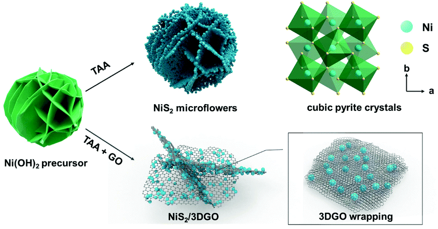 | ||
| Fig. 1 Schematic illustration of the synthesis process for NiS2/3DGO and NiS2 MF and the proposed stabilizing effects of 3DGO on the NiS2 electrode. | ||
XRD patterns were investigated to detect the phase and crystal structure information of the finally obtained samples (Fig. 2a). All characteristic diffraction peaks of both NiS2 MF and NiS2/3DGO can be well indexed with cubic pyrite NiS2 (JCPDS No. 89-3058), manifesting the as-prepared Ni(OH)2 precursor does successfully convert into NiS2 after long-time sulfurization. No distinct diffraction peak located at 22.5° resulting from the (002) plane of the graphene nanosheets was detected in NiS2/3DGO. This phenomenon was caused by the growth of nanocrystalline NiS2 on the GO sheet surface, thus preventing the re-stacking of the GO sheet and covering the weak GO signal.44 Meanwhile, based on Scherer's formula, the size of the NiS2 nanoparticles can be further reckoned to be in the range of 100–120 nm, which in accordance with the particle size statistics shown in Fig. S3.† For NiS2/3DGO, two weak Raman peaks are detected at 289 and 490 cm−1, which is attributed to Eg and Ag modes of NiS2, respectively.45,46 Besides, the Raman peaks at 1353 and 1608 cm−1 are assigned to the D-band and G-band in GO.47 The intensity ratio (ID/IG) of these two adjacent peaks is about 1.24 and lower than that of the 3DGO (1.44), confirming that more defects and disorder exists in the NiS2/3DGO structure.31 Meanwhile, the D and G peaks of 3DGO samples are shifted toward lower wavenumbers compared to those of NiS2/3DGO samples, manifesting that the number of GO layers in 3DGO has increased significantly (Fig. 1b). This phenomenon further illustrates the fact that the presence of NiS2 nanoparticles can effectively suppress the shrinkage of the GO layer.
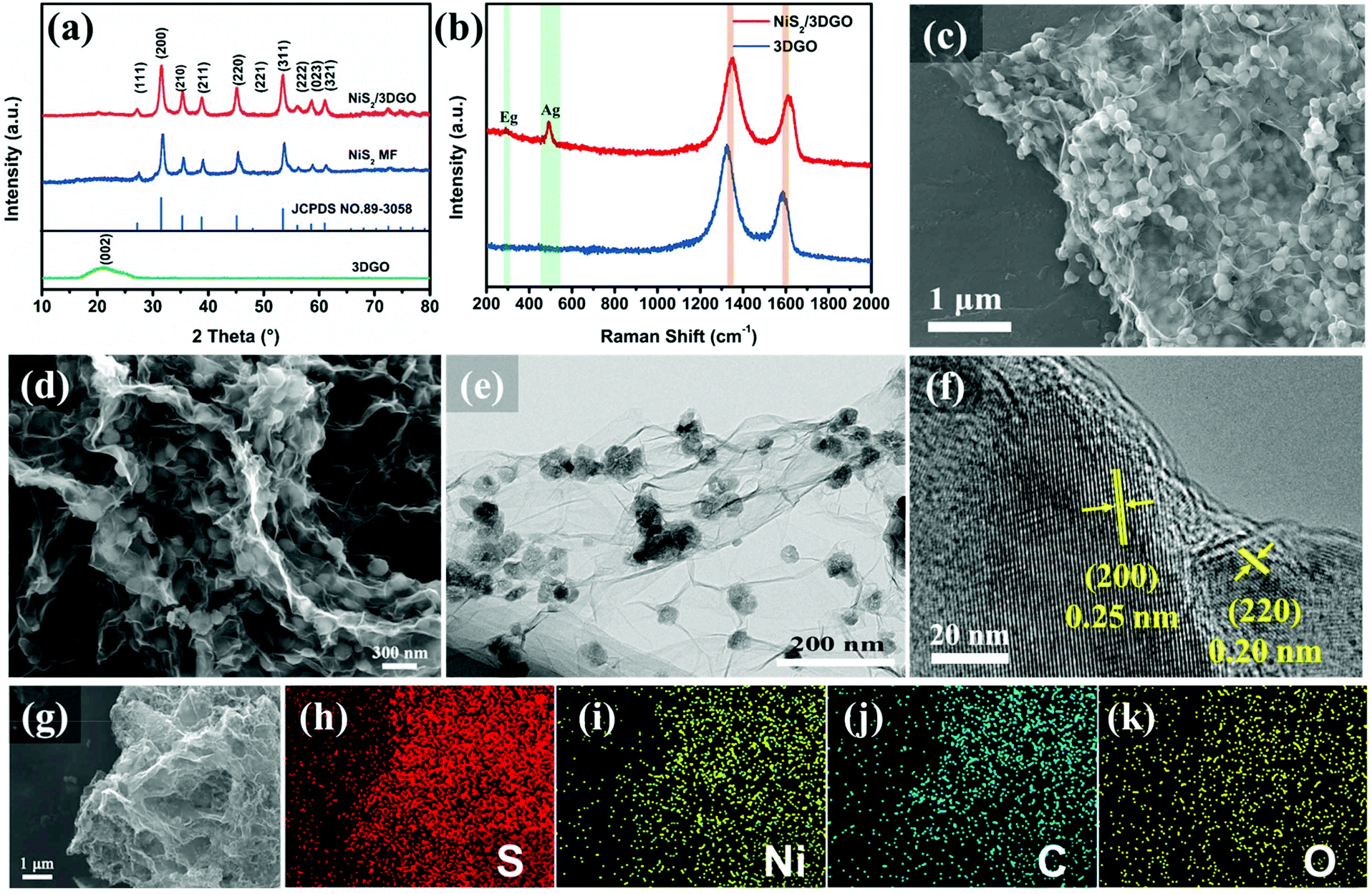 | ||
| Fig. 2 (a) XRD comparison of NiS2/3DGO, NiS2 MF and 3DGO; (b) Raman spectrum of NiS2/3DGO and 3DGO; (c and d) Representative SEM images of NiS2/3DGO; (e and f) TEM and HRTEM images of NiS2/3DGO; (g–k) SEM images and corresponding elemental mapping analysis of NiS2/3DGO. | ||
The microscopic morphology of the NiS2/3DGO is shown in Fig. 2c–f. Reprehensive SEM and TEM images show that NiS2/3DGO composite exhibits a 3D interconnected structure and NiS2 nanoparticles in situ nucleated and grown on the layers of the 3DGO substrate during the self-assembly process (Fig. 2c–e). Moreover, high-resolution TEM shows that the lattice fringes of NiS2/3DGO exhibit interplanar spacings of 0.25 nm and 0.20 nm, which corresponds to the (200) and (220) planes of NiS2, respectively (Fig. 2f). The corresponding elemental mapping of NiS2/3DGO verifies that the Ni, S, C, and O elements were uniformly distributed in the hierarchical 3D interconnected structure (Fig. 2g–k and Fig. S4†).
The content of 3DGO in the as-prepared NiS2/3DGO electrode was investigated by thermogravimetric analysis (TGA, Fig. S5†). The weight loss (2.92 wt%) occurring below 150 °C results in the vaporization of adsorbed water.48 This part should be deducted during the calculation to reflect the authenticity of the result accurately. In the following stage, the weight loss and weight gain can be ascribed to the decomposition of 3DGO and the oxidation of NiS2, respectively. Accordingly, the mass ratio of 3DGO in the NiS2/3DGO composite is calculated to be 9.86%.
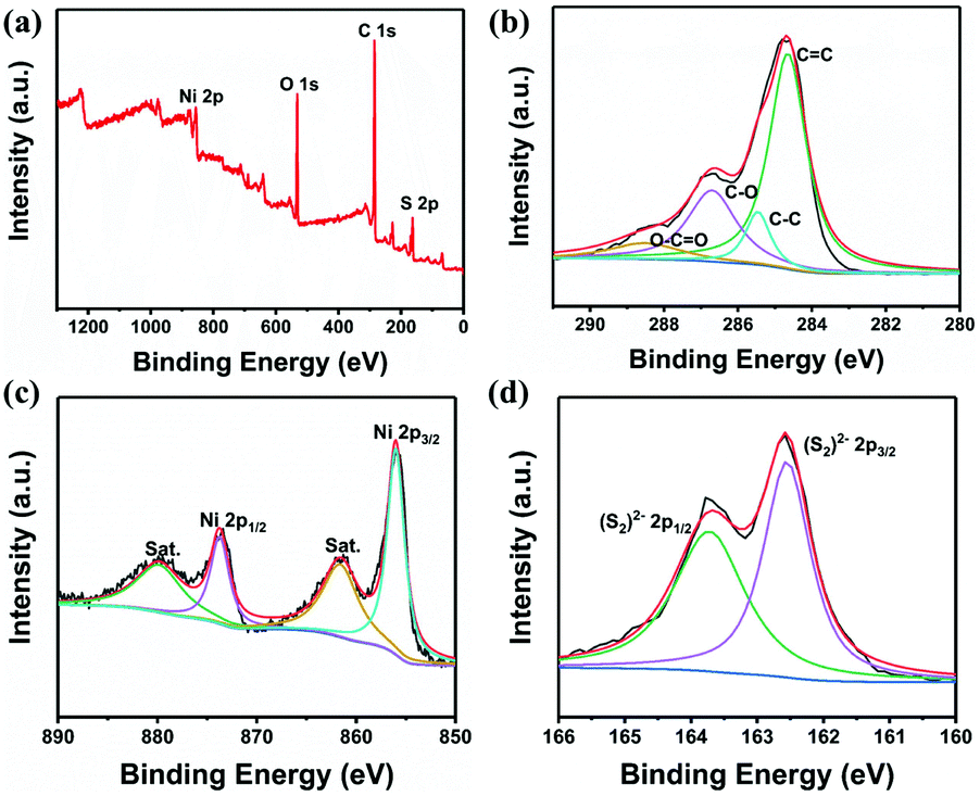
The surface chemical bonding states of Ni, S, C, and O in NiS2/3DGO were further examined by XPS (Fig. 3a). Four peaks recorded at 284.6, 285.5, 286.7, and 288.6 eV can be separated from the C 1s spectrum (Fig. 3b), which corresponds to C![[double bond, length as m-dash]](https://www.rsc.org/images/entities/char_e001.gif) C, C–C, C–O, and O–CO groups, respectively.49,50 This further proved the existence of GO in NiS2/3DGO. In Fig. 3c, two pairs of peaks can be detected at 856 and 874 eV, which is in agreement with 2p3/2 and 2p1/2 of Ni in cubic pyrite NiS2.41 Moreover, the S 2p spectra could be fitted to two adjacent peaks at 162.5 and 163.7 eV that is ascribed to 2p3/2 and 2p1/2 peaks for S22−, respectively (Fig. 3d).
C, C–C, C–O, and O–CO groups, respectively.49,50 This further proved the existence of GO in NiS2/3DGO. In Fig. 3c, two pairs of peaks can be detected at 856 and 874 eV, which is in agreement with 2p3/2 and 2p1/2 of Ni in cubic pyrite NiS2.41 Moreover, the S 2p spectra could be fitted to two adjacent peaks at 162.5 and 163.7 eV that is ascribed to 2p3/2 and 2p1/2 peaks for S22−, respectively (Fig. 3d).
 | ||
| Fig. 3 (a) The XPS survey spectra of NiS2/3DGO; (b) C 1s; (c) Ni 2p; (d) S 2p. | ||
The electrochemical tests of the NiS2 MF and NiS2/3DGO hybrid electrode for potassium ion storage were evaluated ranging from 0.01 to 2.0 V (vs. K+/K). A noticeable reduction peak appeared at ∼1.0 V and disappeared in the subsequent cycles during the initial negative scan process (Fig. 4a). This process was ascribed to an amorphous intermediate phase KxNiS2 formed due to the original cubic NiS2 lattice break and reconstructed during K+ intercalation.51 The following two reduction peaks at 0.68 V and 0.55 V are ascribed to the irreversible solid-electrolyte interface film (SEI) and the further conversion process of K+ with KxNiS2, respectively. For the reversed positive scan, two distinct peaks are detected at 1.18 V and 1.87 V, which are attributed to the conversion reaction of Ni0 + K2S4 to form KxNiS2 and the further extraction of K+ to form amorphous NiS2, respectively. Both the oxidation peak and the reduction peak shifted slightly in the subsequent cycles, which indicates that an activation process may occur in the initial cycle,52 thereby achieving better K+ transport kinetics.
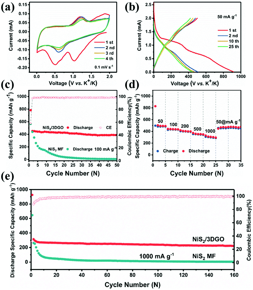 | ||
| Fig. 4 (a) CV test result for the initial four cycles of NiS2/3DGO at 0.1 mV s−1. (b) Representative galvanostatic discharge/charge curves of NiS2/3DGO at 50 mA g−1. (c) Cycling performance of NiS2/3DGO and NiS2 MF at 100 mA g−1. (d) Rate performance of NiS2/3DGO at a different density. (e) Long-term cycling stability of NiS2/3DGO at 1000 mA g−1. | ||
Fig. 4b and Fig. S6† show the comparison of galvanostatic discharge/charge (GDC) curves of the NiS2/3DGO composite and NiS2 MF anode at 50 mA g−1, respectively. The NiS2/3DGO sample showed a distinct higher discharge platform (1.0 V) and a highly consistent GDC curve compared to NiS2 MF (0.8 V) during the charging/discharging process, manifesting that NiS2/3DGO has much less polarization and better capacity retention compared to NiS2 MF. According to the cycling performance of NiS2/3DGO and NiS2 MF at 100 mA g−1 (Fig. 4c). The NiS2/3DGO electrode showed a high initial discharge capacity with a reasonable initial coulombic efficiency (ICE) of 59%. The slightly low ICE is relative to the irreversible SEI and the reconstruction of original cubic NiS2 lattice during K+ intercalation.41 The NiS2/3DGO electrode exhibits a high capacity retention of 88% after 50 cycles (compared with the second cycle). However, the cycling curve of NiS2 MF without 3DGO supported shows an inferior cycling performance. Accurately, the NiS2 MF only delivered a specific capacity of 793.5 mA h g−1 with poor cycling performance. This result further demonstrates that the presence of the elastic GO protective layer dramatically enhances the structural stability of NiS2/3DGO and makes full use of the transport capacity of individual NiS2 nanoparticle.
When gradually increasing the current density at rate stages of 50, 100, 200, 500, and 1000 mA g−1, the GDC curves remain stable and keep reversible capacities of 494, 398, 339, 283, and 235 mA h g−1, respectively. When returning to 50 mA g−1, the NiS2/3DGO quickly recovers to a high specific capacity of 477 mA h g−1 (about 97% capacity recovery rate). Moreover, NiS2/3DGO still showed an excellent capacity retention of 260 mA h g−1 after 160 cycles and high CE of approximately 100% at each cycle (Fig. 4e), far beyond the reversibility of NiS2 MF (<20 mA h g−1 after 50 cycles). Meanwhile, pioneering studies of typical transition metal sulphides were compared with our work. As shown in Table S1† and Fig. S7,† the obtained NiS2/3DGO electrode had a competitive electrochemical performance in KIBs. Especially in the term of capacity, which is much better than those previously reported metal sulphide anodes. The EIS results verify that after the first discharge/charge, the impedance decreases significantly (Fig. S8†). After short activation, the impedance remained stable after 10, 30, and 50 cycles, which further proves that the NiS2/3DGO electrode has a stable interface structure.
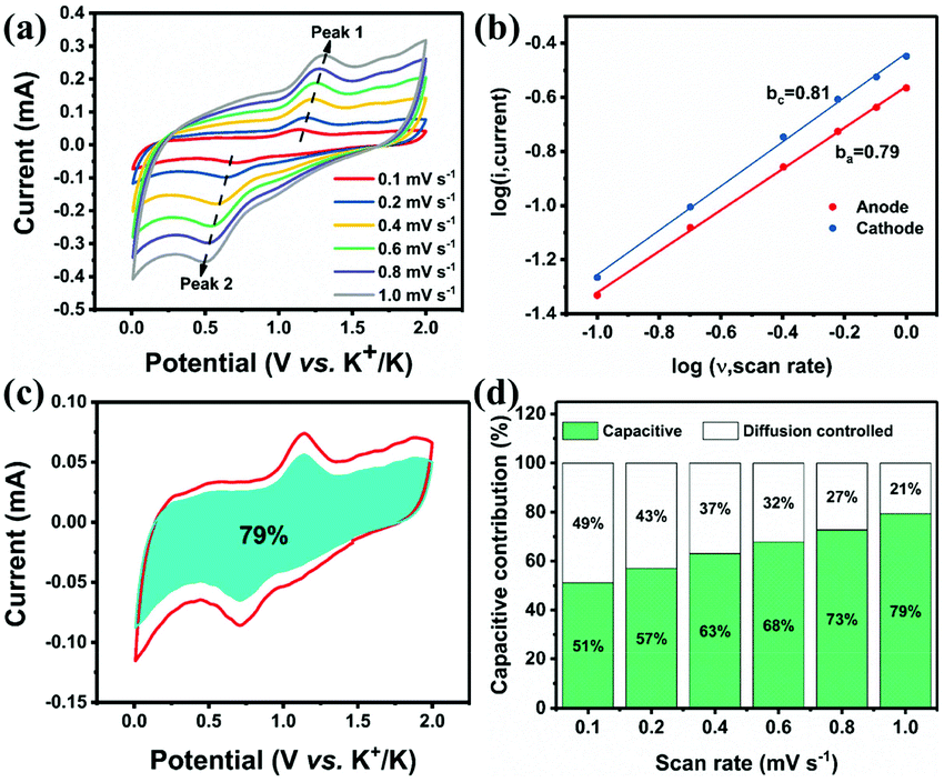
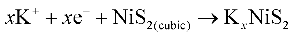
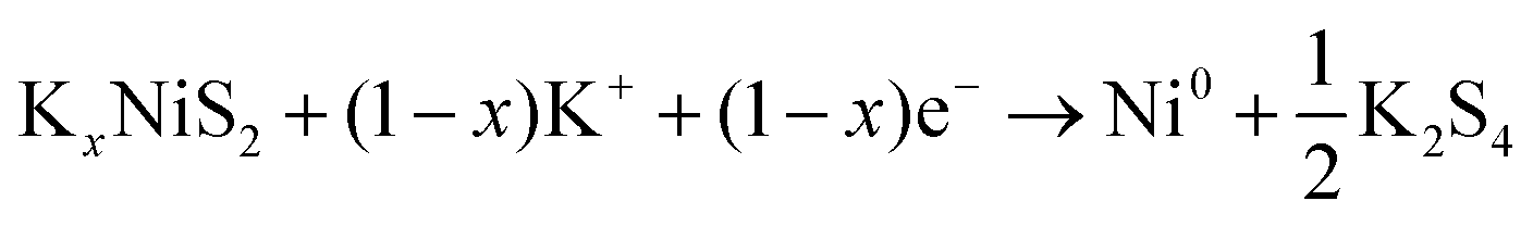
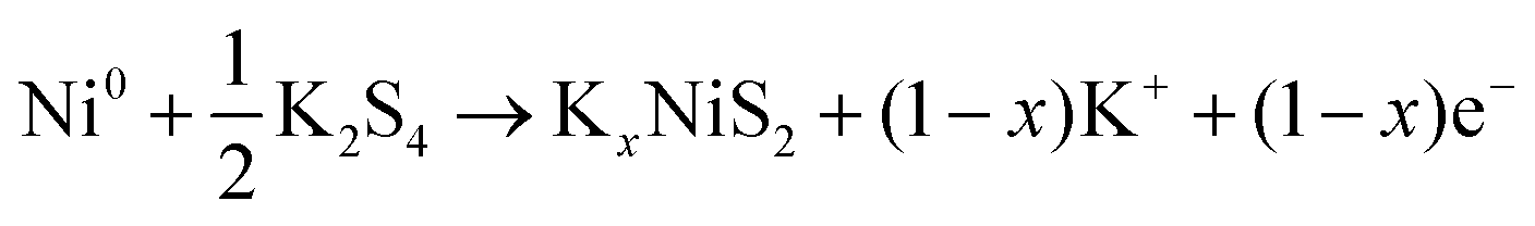
The kinetic research based on CV analysis at scan rates of 0.1 to 1.0 mV s−1 is employed to acquire a deeper understanding of the outstanding rate performance of NiS2/3DGO. Fig. 5a shows that the CV curve at each scanning speed shows similar peak positions and gradually broadened as the scan rate increases. These observations indicate that the NiS2/3DGO electrode has typical pseudocapacitive potassium storage and excellent surface-dominated characteristics, allowing for ultra-fast potassium ion insertion and extraction. A general method to measure the degree of pseudocapacitive effect is to make a qualitative analysis based on the following equation: i = avb, where a and b are constants.53 Generally, for the ideal Faraday intercalation process controlled by the diffusion effect, the b value is 0.5; for a surface-dominated process without diffusion control, the b value is 1.0.15 Hence, the higher b-value of NiS2/3DGO (0.81/0.76) was determined by the cathodic/anodic peaks, suggesting a more favoured surface capacitance-dominated process of NiS2/3DGO (Fig. 5b). Moreover, by further dividing the response current at the same potential into a surface-dominated process (k1ν) and a diffusion-dependent process (k2ν1/2) as the following equation: i = k1ν + k2ν1/2, the percentage of capacitive contribution can be quantified. In consequence, 79% of the total capacity can be considered to be the capacitance contribution of the NiS2/3DGO electrode at a scan rate of 1.0 mV s−1, explaining the fundamental reason for the excellent rate performance of NiS2/3DGO (Fig. 5c). Fig. 5d shows the investigation of the contribution of capacitance at all scan rates. As expected, the capacitance contribution is gradually increasing along with the scan rate. Such excellent pseudo-capacitive storage behaviour is primarily related to the abundant topological defects and excellent conductivity on the GO surface. It can maximize the surface charge storage and effectively improve the rapid pseudocapacitive processes at the interface between NiS2 and the electrolyte.54
 | ||
| Fig. 5 (a) CV curves of NiS2/3DGO at scan rates range from 0.1 to 1.0 mV s−1. (b) Linear relationship of log(i) vs. log(v). The contribution ratio of the capacitive capacities and diffusion-limited capacities at 1 mV s−1 (c) and at different scan rates (d). | ||
In order to further reveal the phase transition process, in situ XRD analysis was performed. Fig. 6a shows that the as-fabricated NiS2/3DGO electrode exhibits the characteristic peaks of (200), (210) and (211) at 31.5°, 35.3°, and 38.8°, respectively. When the cell discharged to 1.0 V, the intensity of each diffraction peak decreased clearly, suggesting that K+ is gradually inserted into the NiS2 host material along with an intermediate phase KxNiS2 formation (Fig. 6a and Fig. S9†). The standard peak of NiS2 disappears when discharged to 0.8 V. Simultaneously, an obvious peak well consistent with K2S4 (JCPDS No. 43-0795) appeared at about 30.9°. The final product is K2S4 instead of K2S, while Li2S/Na2S (analog of K2S) is usually formed in LIBs/NIBs,51,55 manifesting that the conversion reaction occurs and a new phase K2S4 and Ni0 formation. No obvious metallic Ni characteristic diffraction peaks were observed in XRD. The reasonable interpretation is that the in situ formed Ni nanoparticles that are presumably smaller than the X-ray coherence length.56 Moreover, no significant peak was observed during the subsequent charging process, suggesting an irreversible amorphous phase transition accompanied by the destruction of the original cubic NiS2 lattice during K+ intercalation. To confirm this point, ex situ Raman analysis was performed at different stages. As shown in Fig. 6b, with the progress of discharge, the intensity of NiS2 characteristic peak reflection at 490 cm−1 disappeared. Then, a broadening peak is observed when charged to 1 V, demonstrating that the original ordered cubic phase NiS2 (denoted as NiS2(cubic)) transformed into a disordered amorphous phase NiS2 (denoted as NiS2(amorphous)), which is consistent with the test results of in situ XRD. The Raman peak at around 245 cm−1 was not detected, which may be ascribed to the addition of acetylene black and the binder reduced the Raman intensity of the original material. Interestingly, an additional Raman peak at 969.1 cm−1 was detected when discharged to 0.1 V and kept persisting in the subsequent charging process, which may correspond to the SEI film formed during the initial cycle.57 Therefore, the overall reaction process in the initial cycle was proposed as the following equation (Fig. 6c):
During the discharging process:
From OCV to 1.0 V:
 | (1) |
From 1.0 V to 0.2 V:
 | (2) |
During the charging process:
From 0.2 V to 1.2 V:
 | (3) |
From 1.2 V to 2.0 V:
 | (4) |
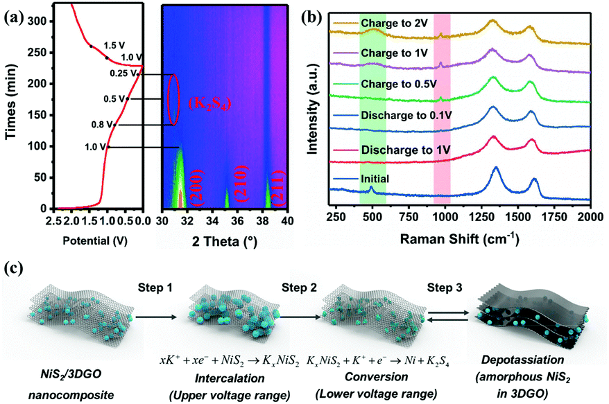 | ||
| Fig. 6 (a) In situ XRD results of NiS2/3DGO during the first cycle at the cut-off voltage of 0.01–2.0 V. (b) Ex situ Raman spectrum of NiS2/3DGO at different discharged/charged states. (c) Schematic illustration of the potassium storage mechanism. | ||
Conclusions
In summary, a self-adaptive strain-relaxed NiS2/3DGO hybrid electrode was fabricated through in situ sulfurization and self-assembly processes. NiS2/3DGO presents a well-defined 3D conductive network in which 3DGO provides rich electronic conductive channels and effectively improves the rapid pseudocapacitive processes at the interface between NiS2 nanoparticles and the electrolyte. Besides, the high flexibility and elasticity GO layer can be self-adaptive to the volumetric change of NiS2. When applied in PIBs, NiS2/3DGO exhibits high specific reversible capacity (451 mA h g−1 at 50 mA g−1), good cycling stability (260 mA h g−1 at 1000 mA g−1 after 160 cycles), and excellent rate performance (97% recovery ratio). Furthermore, the combination of in situ XRD and ex situ Raman observations confirmed that NiS2 undergoes a deep conversion reaction of KxNiS2 to form K2S4 and Ni0 during the initial cycle. This study describes the great potential of the NiS2/3DGO electrode applied in PIBs and gives directions to design novel high-performance electrode materials.Conflicts of interest
There are no conflicts to declare.Acknowledgements
This work was supported by the National Natural Science Foundation of China (51832004 and 21905218), the Natural Science Foundation of Hubei Province (2019CFA001) and the Fundamental Research Funds for the Central Universities (WUT: 203114001).Notes and references
- S. Chu, Y. Cui and N. Liu, Nat. Mater., 2017, 16, 16–22 CrossRef PubMed.
- Q. Liu, X. Su, D. Lei, Y. Qin, J. Wen, F. Guo, Y. A. Wu, Y. Rong, R. Kou, X. Xiao, F. Aguesse, J. Bareño, Y. Ren, W. Lu and Y. Li, Nat. Energy, 2018, 3, 936–943 CrossRef CAS.
- M. Li, J. Lu, Z. Chen and K. Amine, Adv. Mater., 2018, 30, 1800561 CrossRef PubMed.
- J. C. Pramudita, D. Sehrawat, D. Goonetilleke and N. Sharma, Adv. Energy Mater., 2017, 7, 1602911 CrossRef.
- Y. Chen, L. Qin, Y. Lei, X. Li, J. Dong, D. Zhai, B. Li and F. Kang, ACS Appl. Mater. Interfaces, 2019, 11, 45578–45585 CrossRef CAS PubMed.
- W. Zhang, Y. Liu and Z. Guo, Sci. Adv., 2019, 5, eaav7412 CrossRef PubMed.
- Z. Jian, W. Luo and X. Ji, J. Am. Chem. Soc., 2015, 137, 11566–11569 CrossRef CAS PubMed.
- T. T. Shan, S. Xin, Y. You, H. P. Cong, S. H. Yu and A. Manthiram, Angew. Chem., Int. Ed., 2016, 55, 12783–12788 CrossRef CAS PubMed.
- K. Share, A. P. Cohn, R. Carter, B. Rogers and C. L. Pint, ACS Nano, 2016, 10, 9738–9744 CrossRef CAS PubMed.
- H. Gao, T. Zhou, Y. Zheng, Q. Zhang, Y. Liu, J. Chen, H. Liu and Z. Guo, Adv. Funct. Mater., 2017, 27, 1702634 CrossRef.
- V. Lakshmi, Y. Chen, A. A. Mikhaylov, A. G. Medvedev, I. Sultana, M. M. Rahman, O. Lev, P. V. Prikhodchenko and A. M. Glushenkov, Chem. Commun., 2017, 53, 8272–8275 RSC.
- B. Jia, Q. Yu, Y. Zhao, M. Qin, W. Wang, Z. Liu, C.-Y. Lao, Y. Liu, H. Wu, Z. Zhang and X. Qu, Adv. Funct. Mater., 2018, 28, 1803409 CrossRef.
- D. S. Bin, X. J. Lin, Y. G. Sun, Y. S. Xu, K. Zhang, A. M. Cao and L. J. Wan, J. Am. Chem. Soc., 2018, 140, 7127–7134 CrossRef CAS PubMed.
- W. Wang, J. Zhou, Z. Wang, L. Zhao, P. Li, Y. Yang, C. Yang, H. Huang and S. Guo, Adv. Energy Mater., 2018, 8, 1701648 CrossRef.
- Y. Xu, C. Zhang, M. Zhou, Q. Fu, C. Zhao, M. Wu and Y. Lei, Nat. Commun., 2018, 9, 1720 CrossRef PubMed.
- Y. Chen, L. Qin, Y. Lei, X. Li, J. Dong, D. Zhai, B. Li and F. Kang, ACS Appl. Mater. Interfaces, 2019, 11, 45578–45585 CrossRef CAS PubMed.
- A. J. Naylor, M. Carboni, M. Valvo and R. Younesi, ACS Appl. Mater. Interfaces, 2019, 11, 45636–45645 CrossRef CAS PubMed.
- Y. Zhao, X. Ren, Z. Xing, D. Zhu, W. Tian, C. Guan, Y. Yang, W. Qin, J. Wang, L. Zhang, Y. Huang, W. Wen, X. Li and R. Tai, Small, 2019, 16, 1905789 CrossRef PubMed.
- Y. Lei, D. Han, J. Dong, L. Qin, X. Li, D. Zhai, B. Li, Y. Wu and F. Kang, Energy Storage Mater., 2020, 24, 319–328 CrossRef.
- Q. Yao, J. Zhang, J. Li, W. Huang, K. Hou, Y. Zhao and L. Guan, J. Mater. Chem. A, 2019, 7, 18932–18939 RSC.
- J. Li, N. Zhuang, J. Xie, X. Li, W. Zhuo, H. Wang, J. B. Na, X. Li, Y. Yamauchi and W. Mai, Adv. Energy Mater., 2020, 10, 1903455 CrossRef CAS.
- J. Xie, X. Li, H. Lai, Z. Zhao, J. Li, W. Zhang, W. Xie, Y. Liu and W. Mai, Angew. Chem., Int. Ed., 2019, 58, 14740 CrossRef CAS PubMed.
- Q. Yao, J. Zhang, J. Li, W. Huang, K. Hou, Y. Zhao and L. Guan, J. Mater. Chem. A, 2019, 7, 18932–18939 RSC.
- X. Ou, J. Li, F. Zheng, P. Wu, Q. Pan, X. Xiong, C. Yang and M. Liu, J. Power Sources, 2017, 343, 483–491 CrossRef CAS.
- X. Ou, X. Liang, F. Zheng, P. Wu, Q. Pan, X. Xiong, C. Yang and M. Liu, Electrochim. Acta, 2017, 258, 1387–1396 CrossRef CAS.
- P. Ge, H. Hou, S. Li, L. Yang and X. Ji, Adv. Funct. Mater., 2018, 28, 1801765 CrossRef.
- Z. Li, J. Zhang, Y. Lu and X. W. D. Lou, Sci. Adv., 2018, 4, eaat1687 CrossRef PubMed.
- J. Lu, Z. Chen, F. Pan, Y. Cui and K. Amine, Electrochem. Energy Rev., 2018, 1, 35–53 CrossRef CAS.
- Y. Han, W. Li, K. Zhou, X. Wu, H. Wu, X. Wu, Q. Shi, G. Diao and M. Chen, ChemNanoMat, 2020, 6, 132–138 CrossRef CAS.
- J. Zhou, L. Wang, M. Yang, J. Wu, F. Chen, W. Huang, N. Han, H. Ye, F. Zhao, Y. Li and Y. Li, Adv. Mater., 2017, 29, 1702061 CrossRef PubMed.
- X. Xiong, C. Yang, G. Wang, Y. Lin, X. Ou, J.-H. Wang, B. Zhao, M. Liu, Z. Lin and K. Huang, Energy Environ. Sci., 2017, 10, 1757–1763 RSC.
- K. Liang, K. Marcus, S. Zhang, L. Zhou, Y. Li, S. T. De Oliveira, N. Orlovskaya, Y.-H. Sohn and Y. Yang, Adv. Energy Mater., 2017, 7, 1701309 CrossRef.
- Q. Zou, Z. Liang, G. Y. Du, C. Y. Liu, E. Y. Li and Y. C. Lu, J. Am. Chem. Soc., 2018, 140, 10740–10748 CrossRef CAS PubMed.
- Q. Chen, S. Sun, T. Zhai, M. Yang, X. Zhao and H. Xia, Adv. Energy Mater., 2018, 8, 1800054 CrossRef.
- Z. Zhao, Z. Hu, H. Liang, S. Li, H. Wang, F. Gao, X. Sang and H. Li, ACS Appl. Mater. Interfaces, 2019, 11, 44333–44341 CrossRef CAS PubMed.
- B. Chen, Y. Meng, F. Xie, F. He, C. He, K. Davey, N. Zhao and S. Z. Qiao, Adv. Mater., 2018, 30, 1804116 CrossRef PubMed.
- X. Wei, X. Wang, X. Tan, Q. An and L. Mai, Adv. Funct. Mater., 2018, 28, 1804458 CrossRef.
- Y. Fang, X.-Y. Yu and X. W. D. Lou, Matter, 2019, 1, 90–114 CrossRef.
- A. Singh and V. Kalra, J. Mater. Chem. A, 2019, 7, 11613–11650 RSC.
- L. Wang, G. Yang, S. Peng, J. Wang, W. Yan and S. Ramakrishna, Energy Storage Mater., 2019, 25, 443–476 CrossRef.
- L. Yang, W. Hong, Y. Zhang, Y. Tian, X. Gao, Y. Zhu, G. Zou, H. Hou and X. Ji, Adv. Funct. Mater., 2019, 29, 1903454 CrossRef CAS.
- W. Konicki, M. Aleksandrzak and E. Mijowska, Pol. J. Chem. Technol., 2017, 19, 120–129 CAS.
- Y. Zhu, S. Murali, W. Cai, X. Li, J. W. Suk, J. R. Potts and R. S. Ruoff, Adv. Mater., 2010, 22, 3906–3924 CrossRef CAS PubMed.
- Q. Chen, W. Chen, J. Ye, Z. Wang and J. Y. Lee, J. Power Sources, 2015, 294, 51–58 CrossRef CAS.
- T. Suzuki, K. Uchinokura, T. Sekine and E. Matsuura, Solid State Commun., 1977, 23, 847–852 CrossRef CAS.
- C. Zhang, Int. J. Electrochem. Sci., 2017, 12, 4610–4618 CrossRef CAS.
- R. Verma, P. N. Didwal, H.-S. Ki, G. Cao and C.-J. Park, ACS Appl. Mater. Interfaces, 2019, 11, 26976–26984 CrossRef CAS PubMed.
- C. Zhang, Y. Xu, M. Zhou, L. Liang, H. Dong, M. Wu, Y. Yang and Y. Lei, Adv. Funct. Mater., 2017, 27, 1604307 CrossRef.
- B. Li, Y. Liu, Y. Li, S. Jiao, S. Zeng, L. Shi and G. Zhang, ACS Appl. Mater. Interfaces, 2020, 12, 2390–2399 CrossRef CAS PubMed.
- J. Zhang, Y. Xu, Z. Liu, W. Yang and J. Liu, RSC Adv., 2015, 5, 54275–54282 RSC.
- G. Zhao, Y. Zhang, L. Yang, Y. Jiang, Y. Zhang, W. Hong, Y. Tian, H. Zhao, J. Hu, L. Zhou, H. Hou, X. Ji and L. Mai, Adv. Funct. Mater., 2018, 28, 1803690 CrossRef.
- D. M. Zhang, J. H. Jia, C. C. Yang and Q. Jiang, Energy Storage Mater., 2020, 24, 439–449 CrossRef.
- D. Chao, P. Liang, Z. Chen, L. Bai, H. Shen, X. Liu, X. Xia, Y. Zhao, S. V. Savilov, J. Lin and Z. X. Shen, ACS Nano, 2016, 10, 10211–10219 CrossRef CAS PubMed.
- Y. Jiang and J. Liu, Energy Environ. Mater., 2019, 2, 30–37 CrossRef.
- X.-C. Liu, Y. Yang, J. Wu, M. Liu, S. P. Zhou, B. D. A. Levin, X.-D. Zhou, H. Cong, D. A. Muller, P. M. Ajayan, H. D. Abruña and F.-S. Ke, ACS Energy Lett., 2018, 3, 1325–1330 CrossRef CAS.
- P. Poizot, S. Laruelle, S. Grugeon, L. Dupont and J. M. Tarascon, Nature, 2000, 407, 496–499 CrossRef CAS PubMed.
- S.-L. Yang, H.-B. Yao, M.-R. Gao and S.-H. Yu, CrystEngComm, 2009, 11, 1383–1390 RSC.
Footnote |
| † Electronic supplementary information (ESI) available. See DOI: 10.1039/d0nr01274b |
| This journal is © The Royal Society of Chemistry 2020 |