
 Open Access Article
 This Open Access Article is licensed under a Creative Commons Attribution-Non Commercial 3.0 Unported Licence
Printed electronics based on inorganic conductive nanomaterials and their applications in intelligent food packaging
Yu
Liao
ab,
Rui
Zhang
a and
Jun
Qian
 *a
*a
aSchool of Printing and Packaging, Wuhan University, Luojia Hill, Wuhan, 430072, China. E-mail: whuqianjun@163.com
bChemical & Environmental Engineering, School of Engineering & Applied Science, Yale University, 17 Hillhouse Avenue, New Haven, CT 06511, USA
First published on 17th September 2019
Abstract
The diverse demands of consumers for packaging functions and increasingly complex product circulation systems have spurred the development of intelligent food packaging (IFP). Besides the basic functions of traditional food packaging, which include the protection of food, sales promotion and convenient transportation, the developing area of IFP can detect the condition of food (ambient temperature, humidity, corruption degree, etc.) in one whole product cycle, and record and feedback information regarding the quality of the packaged food to form a complete product monitoring system. Recently, cutting-edge printed electronics (PE) technology has opened new opportunities for the realization and expansion of IFP functions. Here we introduce some new printed sensors and radio frequency identification (RFID) tags, which are used to form an IFP system. Since conductive ink is the cornerstone of PE, in this paper, the synthesis and properties of inorganic conductive nanomaterials are also reviewed. The formulation of conductive ink, sintering methods and the flexible substrates used in PE are also discussed. Focusing on the state-of-the-art application of PE in the field of IFP, the purpose of this article is to provide a review of IFP that integrates emerging PE technology with prospective next-generation IFP systems to sense, detect, and record feedback information on products in the supply chain environment.
1. Introduction
Detecting the freshness and safety of food has become a significant challenge in the global supply chain and with the demand for minimally processed food products. Therefore, there is a continued demand for new analytical technologies that can detect the ambient environment and freshness of packaged food in a more time-effective manner. The continuing evolution of large-area radio frequency identification (RFID) and printed sensor production is spurred by the development of printed electronics (PE). Once we reduce the cost of such packaging, RFID and printed sensors can be applied to food packaging. The synergistic integration of intelligent food packaging (IFP) with PE technologies, which has transitioned from science fiction to an area of focus, satisfies the need for the protection of food from environmental pollution, and plays an active role in the quality and safety of food. It prolongs the shelf life using functions that traditional packaging cannot realize, for example judging the freshness of food, the authenticity of drugs, the environmental factors (temperature, humidity, light etc.) in circulation, and so on.1–4 Recent trends in IFP include: (i) theoretical research on internal environmental factors of packaging that impair the shelf life of food, such as gas composition, temperature, microorganisms, etc.; (ii) materials or strategies that are optimized to detect changes in products and to provide effective information to the packaging users (consumer or production decision-makers); and (iii) challenges such as cost minimization that still lie ahead. This review is an effort to familiarize readers with the great breakthrough of IFP in protecting food quality and safety in the dynamic and diverse circulation environment.The burgeoning PE technology provides a possibility for the realization of IFP. As an interdisciplinary technology between printing and electronics, PE uses a printing process, such as inkjet printing, screen printing, nanoimprinting or soft lithography, etc. to prepare electronic circuits on a flexible substrate.5–11 To date, low-cost has been the main driving force in the development of the electronics. For a cost-effective and high-volume process, a printing method like the roll-to-roll (R2R) manufacturing platform has been used to fabricate PE that is becoming ultra-light and ultra-thin.8,12 During the past five decades, microelectronics has dominated electronic technology. Table 1 shows the differences between PE and microelectronics. The complexity and huge investment in hard electronic devices made by traditional microelectronic technology is incompatible with the low-cost, high throughput production which is necessary for practical applications in packaging. Conversely, PE can be applied. For example, RFID has been widely used for electronic labeling in packaging.
| PE | Microelectronics | |
|---|---|---|
| Advantages | Light, can be flexible when it prints on flexible substrates, easily distributed, greatly reduced thickness with invariant integration level, low cost | No onerous requirements of mechanical properties, fast running |
| Disadvantages | High requirements for mechanical properties and encapsulation | Heavy, hard and dispersed |
| Manufacturing process | Print, R2R | No mass production, high cost, low efficiency, environmental pollution |
| Substrates | Flexible substrates (plastic, paper, etc.) | Rigid substrates (silicon substrate, glass substrate) |
Conductive ink is the foundation stone for the fabrication of PE and offers good performance as shown in Fig. 1. In this figure, a complete process is illustrated, from the preparation of conductive ink, to the printing process and applications in IFP. The preparation of high-quality conductive ink is a recent research hotspot. Nano-conductive ink is a functional ink developed rapidly with modern science and technology. It is a kind of multi-component dispersion in solvent, containing mainly resins used as a binder to adhere to the substrates, oils as the carrier or medium of the nanomaterial additives to control the rheological properties of the ink, and nanomaterials as the conductive fillers.12–16 In this review, the synthesis and stabilization of two kinds of inorganic conductive nanomaterials (metal nanoparticles (NPs) and carbon nanomaterials), and sintering processes are briefly introduced.
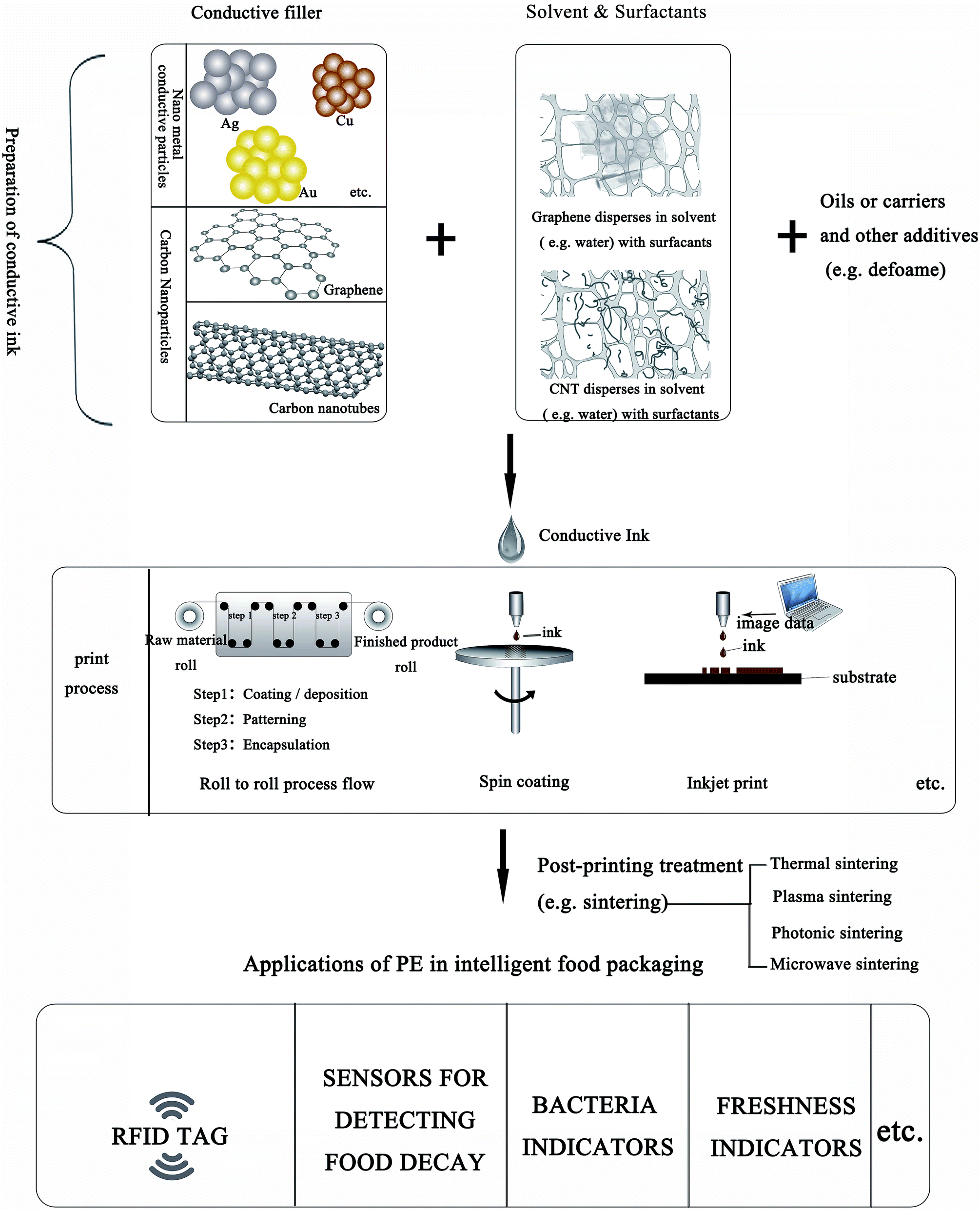 | ||
| Fig. 1 Summary of the preparation of conductive ink based on inorganic conductive nanomaterials, and the applications of PE in IFP. | ||
The review will focus on the latest progress in the utilization of PE for the fabrication of various IFP. The main focus of the present study is the utilization of PE to realize new IFP with diversified functions. We will explore the issues around expanding the diversity of functions while reducing the additional cost of packaging. In brief, parallel activities of laboratory research (developing new applications of PE in IFP) and commercialization (reducing cost and increasing production efficiency) are needed to promote the development of new functions and the commercialization of IFP. We hope that PE can be better integrated into IFP to broaden its application prospects and increase market capacity.
2. Printable conductive nanomaterials
2.1 Conductive ink: requirements and conduction mechanism
The formulations and preparation methods of conductive inks are crucial if they are to demonstrate good printability, with the appropriate viscosity and surface tension as well as adhesion to specified substrates.13,17,18 However, several key characteristics, such as the viscosity and ink particle size, should be adjustable to fit different printing methods. Table 2 (ref. 19) shows a comparison of different printing methods (piezoelectric inkjet printing, aerosol jet printing, screen printing, gravure printing, flexographic printing, gravure offset printing and letterset printing) with respect to several technical parameters (optimum range of viscosity, single printing ink film thickness, pattern resolution and printing speed). It is desirable to prepare nanosheet (NS) and nanoparticle (NP)-based conductive inks with well-enhanced electrical conductivity. There are many factors which can affect the conducting performance of ink, such as its composition and the post-processing methods used. Moreover, the mechanisms, which mainly include percolation, the tunnel effect and the field emission effect, can change with the different ink types and the concentration of conducting fillers. Fig. 2 illustrates the conducting mechanism of conductive ink from the colloid state to solidified film printing on the substrate. The conductive ink remains insulating unless the solvent volatilizes and promotes stable binding between the conductive NPs and the matrix (this process is often denoted as the drying of the ink).| Printing technology | Optimum range of viscosity/cP | Single printing ink film thickness/μm | Pattern resolution/μm | Printing speed/(m2 s−1) |
|---|---|---|---|---|
| Piezoelectric inkjet printing | 5–20 | 0.05–1 | >20 | ≤0.5 |
| Aerosol jet printing | 1–1000 | 0.1–5 | >8 | ≤0.01 |
| Screen printing | 500–10![[thin space (1/6-em)]](https://www.rsc.org/images/entities/char_2009.gif) 000 000 |
≤100 | >50 | 0.1–10 |
| Gravure printing | 50–500 | 0.8–8 | >20 | 3–60 |
| Flexographic printing | 50–200 | 0.8–2.5 | >50 | 3–30 |
| Gravure offset printing | >50 | 0.5–6 | >20 | 0–30 |
| Letterset printing | 50000–150000 |
0.5–1.5 | >50 | 0.5–2 |
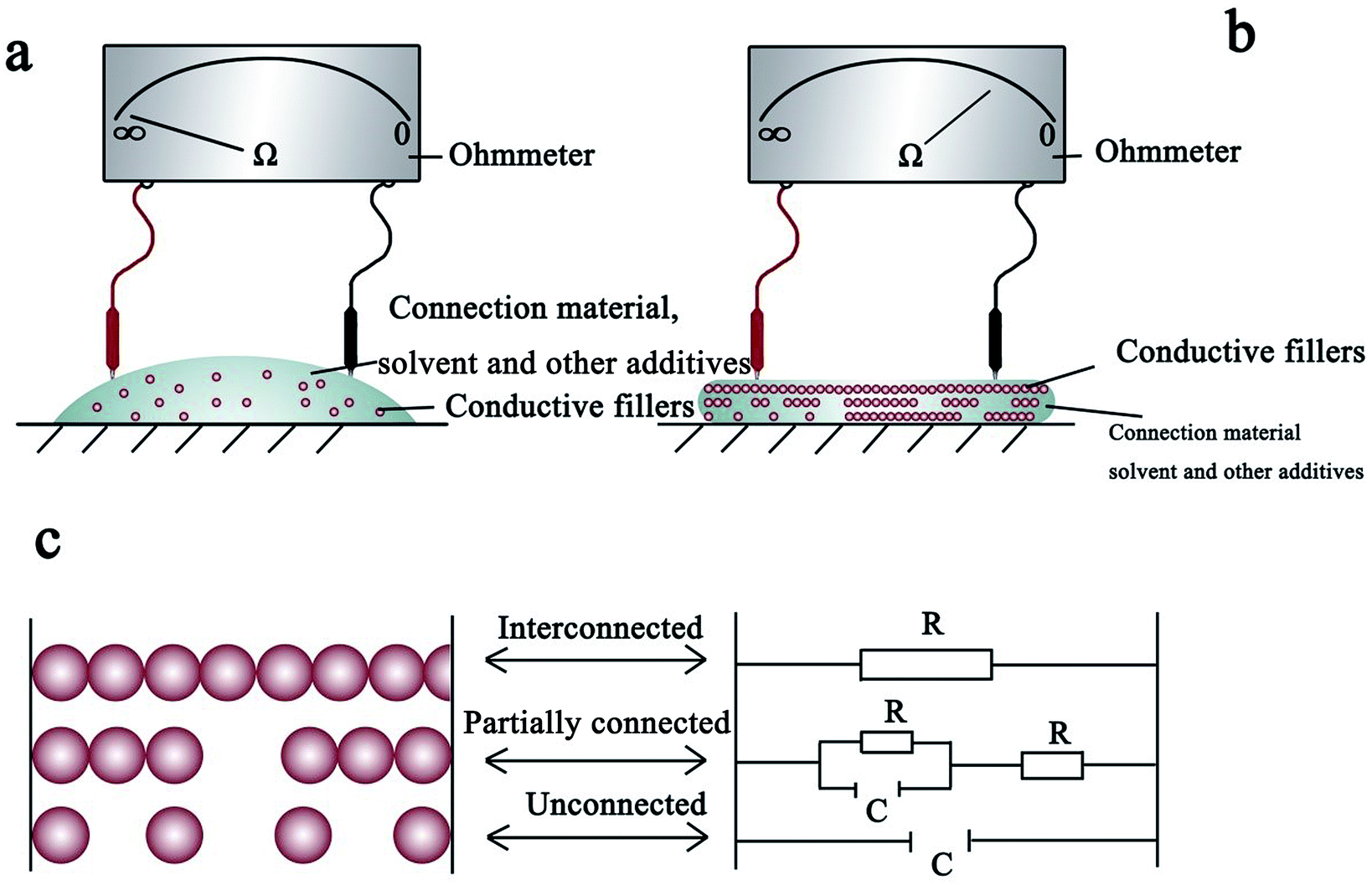 | ||
| Fig. 2 A schematic diagram of the conduction mechanisms of conductive ink: (a) less conductive particles, where the residual solvent barrier between conductive particles and charge transfer resistance are very large, (b) conductive particles in close contact, where the resistance is lower, and (c) the three connection states of the conductive ink. | ||
After the drying of the conductive ink on the substrate, the conductive NPs mainly exist in three states: a continuous contact state forming a current path termed as percolation; a partly continuous contact state, in which thermal vibration causes electrons to drift through the gaps between the NPs and create an electronic pathway (namely, the tunnel effect); and a completely discontinuous state in which the particles cannot form an electronic pathway because of large gaps between the NPs.19–21
2.2 Metal NPs
Top-down methods use physical methods (mechanical grinding, laser ablation, physical vapor deposition, etc.) to break bulk metal into nanoscale particles. The most common method among several top-down methods is physical vapor deposition. The metal vapor is prepared by plasma excitation or thermal heating of the bulk metal, by which the metal wires or metal powders vaporize and condense rapidly through a stream of inert gas like N2 or Ar in the solution. Wang et al.25 have reported the preparation of Ag NPs with sizes between 2 nm and 6 nm by plasma vapor deposition. However, the need for sophisticated equipment and severe operating conditions hamper the commercialization of this high-energy-consumption method.
Conversely, bottom-up routes decompose the precursor in solution or reduce it in the presence of a reducing agent to form a metal ionic liquid which will form unique nanostructures by self-assembly.26Fig. 3 shows the synthetic process for metal NPs using a chemical reduction method. The bottom-up routes make it possible to prepare a large number of different sizes of metal NPs by adjusting parameters such as the types and dosages of the reducing agent, pH and temperature, to affect the growth of the crystals and finally control the sizes, shapes and distribution properties of the products. The most commonly used reductants include borohydride,27 hydrazine,28 ascorbic acid29 and citrate,30etc. Tippabattini Jayaramudu et al.31 have synthesized nano-Ag particles with a uniform average size between 10 and 12 nm using silver nitrate as the precursor and polyethylene glycol as the reducing agent. The advantages of this method which include the production of uniform microstructures and low energy consumption have impelled researchers to put more effort into finding the optimal synthetic parameters. Compared with physical methods, the bottom-up routes are more suitable for the commercial application of IFP.
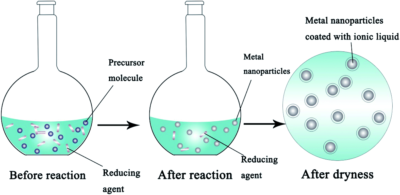 | ||
| Fig. 3 Schematic diagram of the “bottom up” route of metal NP synthesis by a chemical reduction method. | ||
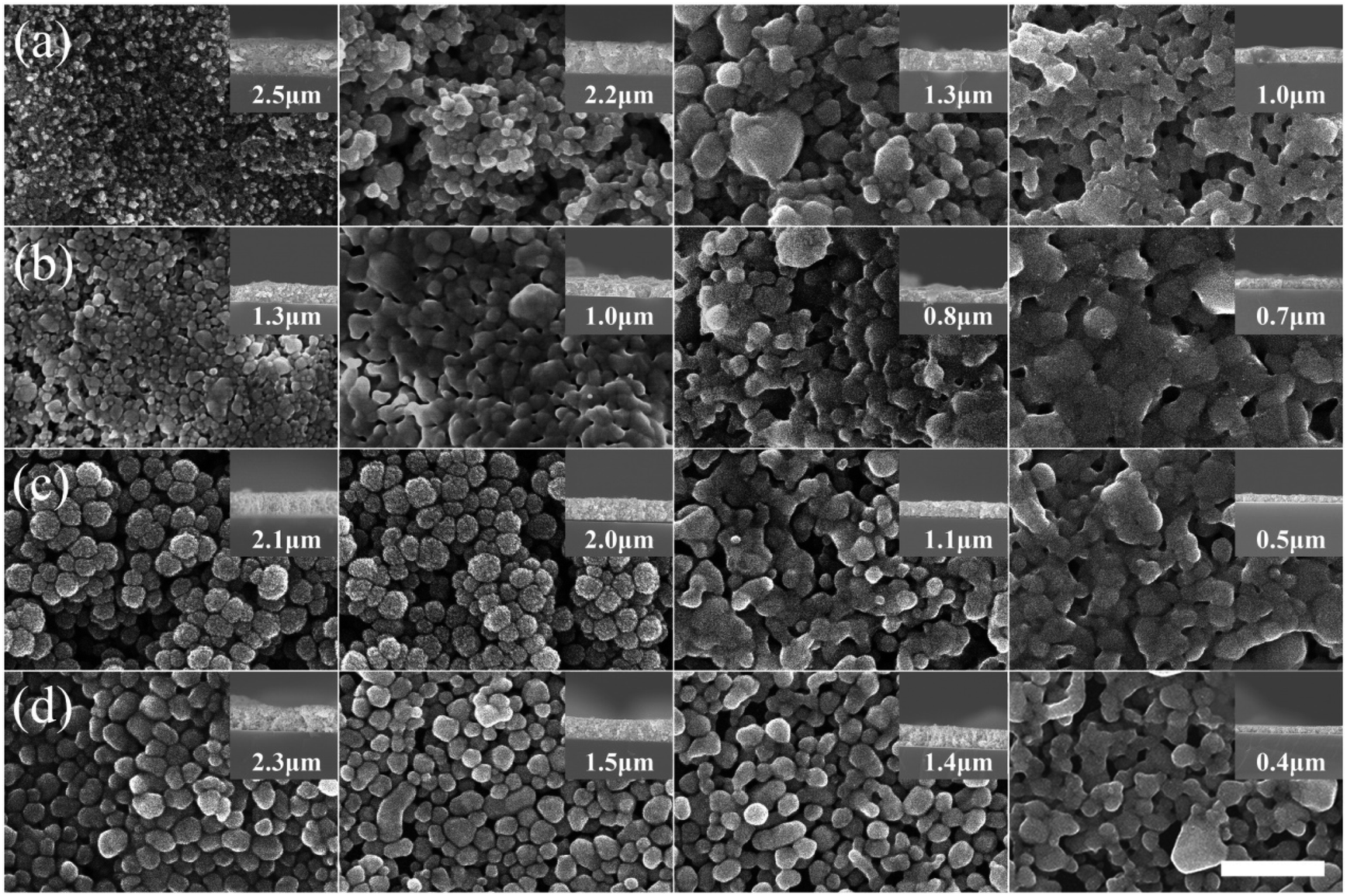 | ||
| Fig. 4 SEM images (top and side views) of nano Ag films: (a) Ag-ND, (b) Ag-HA1, (c) Ag-HA2, and (d) Ag-PVP sintered at various temperatures (left to right: 100 °C, 140 °C, 180 °C, and 220 °C); scale bar = 500 nm [reprinted with permission from ref. 38, M. Seo, J. S. Kim, J. G. Lee, S. B. Kim and S. M. Koo, The effect of silver particle size and organic stabilizers on the conductivity of silver particulate films in thermal sintering processes, Thin Solid Films, 2016, 616, 366–374. Copyright© Elsevier]. | ||
2.3 Carbon NSs and NPs
Because of their excellent chemical, electrical, mechanical, and optical properties as well as their abundance, graphene and carbon nanotubes (CNTs) are emerging as promising candidates for metal NPs.6,9,12,13,18,55–57 Since 2004, more and more of the literature has focused on the preparation of graphene and CNTs. Where and how we can apply graphene in new fields and for new functions has become a wide-spread challenge.Oxidation–exfoliation–reduction is the most commonly reported method used to prepare graphene. As shown in Fig. 5, firstly, strong oxidizers65 are used, such as fuming nitric acid,67,68 potassium perchlorate69 or potassium permanganate70 to oxidize the graphite. Oxygen-containing groups such as carboxyl and hydroxyl are formed, causing an increase in the interlayer distance of graphite from 3.35 Å to 7–10 Å.71–74 The as-prepared graphene oxide (GO) can then easily be exfoliated by ultrasonic treatment, and finally graphene can be prepared by reduction. For example, Hong et al.74 prepared graphene ink with the Hummers' method using hydrazine as a reducing agent under anoxic conditions. Then, they mixed the as-prepared graphene with cellulose acetate, acetone, n-butyl pyridinium hexafluorophosphate and cyclohexanone, and sonicated for a given amount of time. They fabricated electrodes for Cd2+ and Pd2+ determination using the as-prepared graphene ink by screen printing and obtained an excellent transfer resistance (430 Ω). Fig. 5 shows several methods used for synthesizing graphene from graphite, and compares the quality and cost of the graphene products manufactured by the different methods.
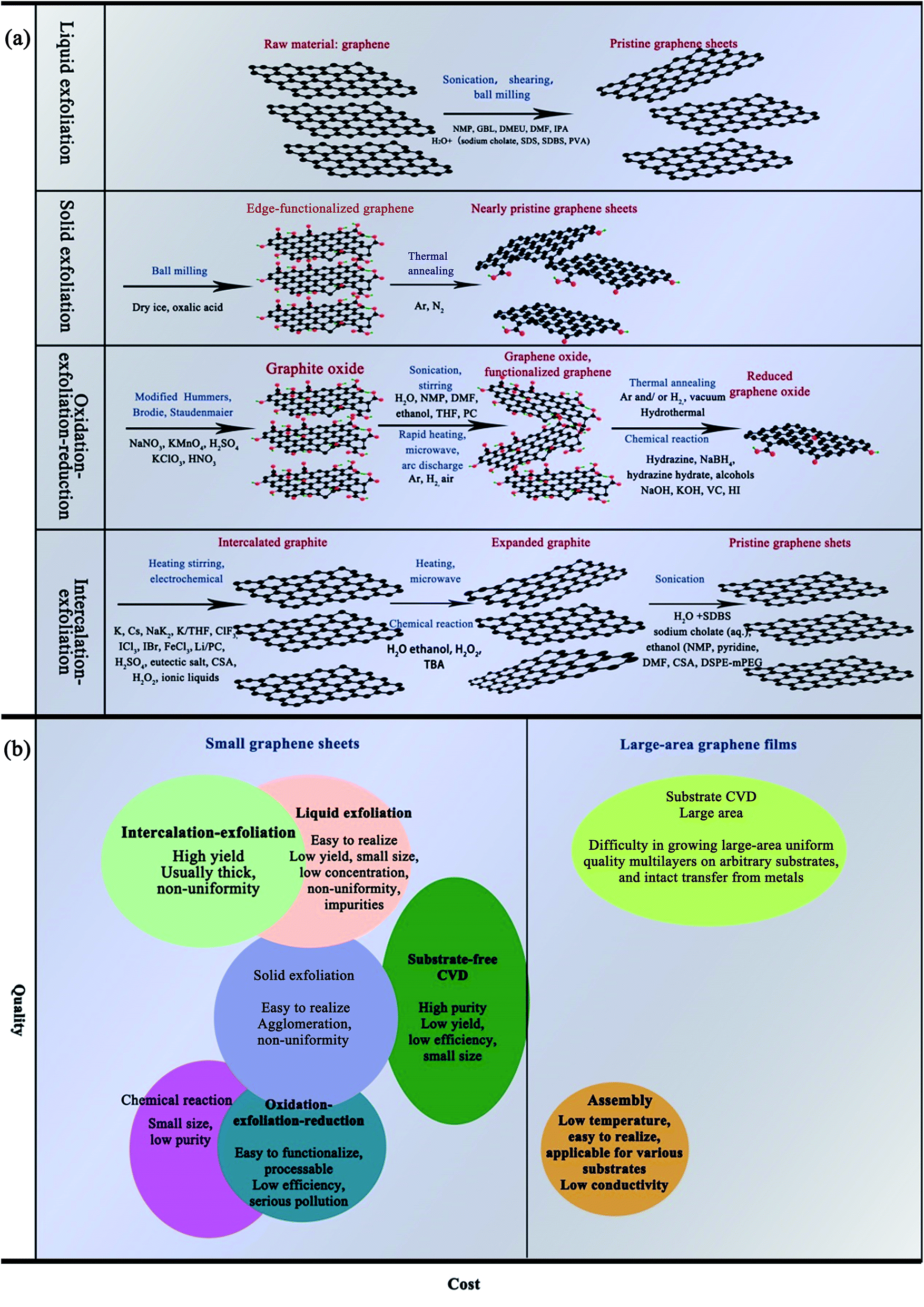 | ||
| Fig. 5 (a) Schematic diagram of the synthesis of graphene from graphite. (b) Comparison of the quality and cost of graphene products manufactured by different methods [reprinted with permission from ref. 75, W. Ren and H. M. Cheng, The global growth of graphene, Nat Nanotechnol, 2014, 9, 726–730. Copyright© Springer Nature]. | ||
LE is another method used to produce graphene. The process involves ultrasonic treatment of the graphite dispersed in solvent followed by centrifugation to obtain graphene.76 Arhin et al.77 prepared inkjet-printed graphene ink using graphene produced by ultrasonic-assisted liquid phase exfoliation. They ultrasonicated 100 mg graphite flakes with 1.5 mg PVP in 10 mL isopropanol for 12 h at 15 °C and then centrifuged at 4000 rpm for 1 h. As shown in Fig. 6, graphene was obtained with an average flake thickness of 5.9 ± 0.2 nm and with 56% of flakes being 4 nm thick. Recently, microfluidization of graphite (which is similar to LE) has been developed by stripping graphite in aqueous solutions with high shear rates. This is a simple and scalable production route for conductive inks for large-area printing in flexible electronics.
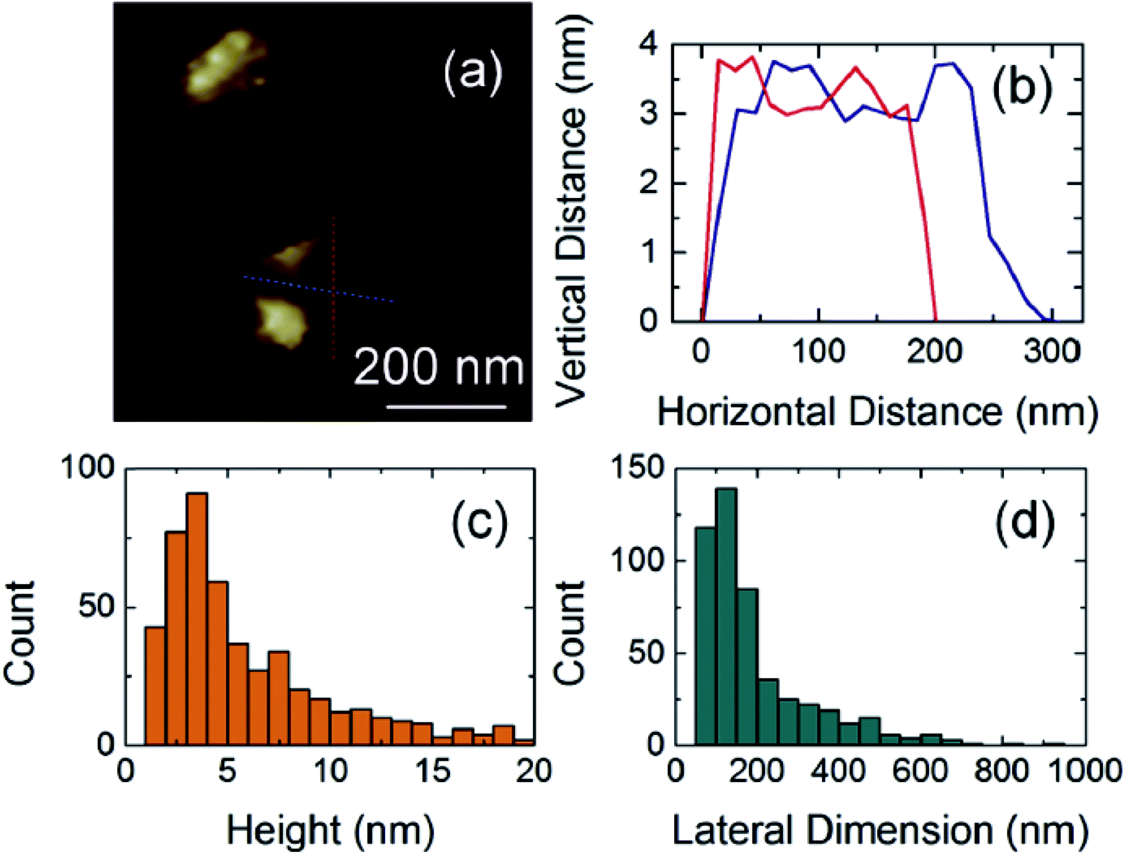 | ||
| Fig. 6 Atomic force microscopy characterization of dispersed graphene flakes: (a) image and (b) section of a typical graphene flake. Distributions of (c) flake thickness and (d) flake lateral dimensions [reprinted with permission from ref. 77, D. Dodoo-Arhin, R. C. T. Howe, G. Hu, Y. Zhang, P. Hiralal, A. Bello, G. Amaratunga and T. Hasan, Inkjet-printed graphene electrodes for dye-sensitized solar cells, Carbon, 2016, 105, 33–41. Copyright© Elsevier]. | ||
Besides, CVD is a method commonly used in industry to produce high-quality graphene sheets with large areas. Osikoya et al. fabricated a CVD graphene sheet grown from acetylene as the carbon source, with a large available surface area, while the sheet resistance was as low as 125 Ω sq−1.78–80 However, the biggest challenges for this technique are the high cost and complex processes involved.
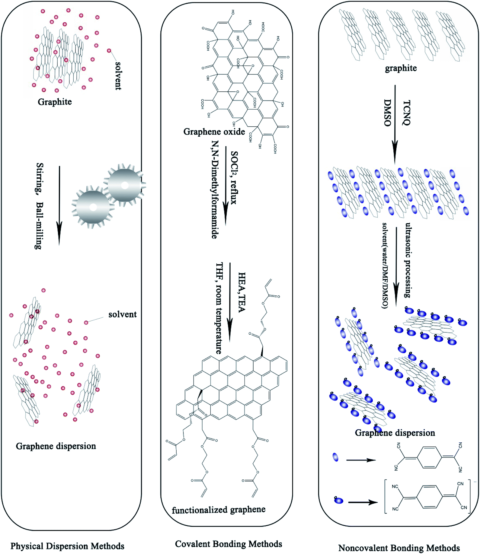 | ||
| Fig. 7 Schematic diagram of the dispersion methods used for graphene. | ||
Physical methods encompass ultrasonic treatment, stirring, and ball-milling. Baomin Wang et al.84 prepared a graphene nanoplatelet suspension by ultrasonic treatment. They used a minimum sonication time to effectively disperse the 0.1 g L−1 concentration of bundled graphene nanoplatelets. Weifeng Zhao et al.85 used ball-milling to exfoliate graphene in a variety of organic solvents such as N,N-dimethylformamide, at a concentration of up to 0.08 mg mL−1, achieving a yield higher than 32.0 wt%. With low cost, simple operation and the possibility of application to large scale production, physical methods are a popular choice among many researchers. However, physical methods cause damage to the structure of graphene and produce a low dispersion rate which is unsatisfactory.
Noncovalent bonding methods based on π–π interactions and surfactant modification can form a stable dispersion of graphene. π–π interactions make use of π bonds in aromatic molecules (polycyclic aromatic hydrocarbons (PAHs), peptides, etc.) to stabilize the graphene dispersion. Jun Wang et al.77 prepared a kind of graphene dispersion using PAHs. They revealed that after loading with PAHs, the conformation and aggregation of the graphene and GO nanosheets dramatically changed. Surfactant addition is the most common way to prepare stable graphene dispersions. To prepare stable conductive ink various surfactants such as PAH and sodium dodecyl sulfate (SDS)86 are needed together with a solvent like water or N-methylpyrrolidone, etc. Song et al.87 prepared a kind of graphene ink powder containing graphene and excess ethyl cellulose (2:3, w/w) dispersed in terpineol with 20% w/v of solid in the solvent. They used this graphene ink to print conductive graphene patterns on plastic with high-resolution (3.2 μm line width and 1 μm spacing) using a transfer printing method. In addition, carbon NSs and NPs will not melt during heat treatment, in contrast to metal NPs, but the dispersants existing in the carbon NSs and NPs need heat treatment for removal. Secor et al.88 heat treated graphene ink at 250 °C for 30 minutes to achieve a resistance of 4 mΩ cm. Lee et al.89 reported that sintering printed graphene NSs (GNSs) at 400 °C could effectively lead to the elimination of excess SDS on the GNSs and increase the C![[double bond, length as m-dash]](https://www.rsc.org/images/entities/char_e001.gif) C content. However, these organic solvents are toxic. Developing non-toxic stabilizing agents and surfactants or modified graphene or CNTs with excellent dispersivity in water has become the subject of many studies in the literature. Michel et al.90 synthesized a kind of surfactant-free graphene ink in a mixture of terpineol and cyclohexanone. Furthermore, the conductive ink had an excellent electrical conductivity with a resistance of only 1.1 mΩ m compared with 7.1 mΩ m for the surfactant-assisted ink (N-methyl-2-pyrrolidone and ethyl cellulose). This formulation is very eco-friendly and has excellent conductivity because of the biomaterials, terpineol and cyclohexanone. Koutsioukis et al.91 recently developed a highly conductive formulation using pristine graphene and dihydroxyphenyl-functionalized MWNTs mixed with another hydrophilic polymer which displayed desirable conductivity (Rs = 22.6 Ω sq−1, σ = 4971 S m−1).
C content. However, these organic solvents are toxic. Developing non-toxic stabilizing agents and surfactants or modified graphene or CNTs with excellent dispersivity in water has become the subject of many studies in the literature. Michel et al.90 synthesized a kind of surfactant-free graphene ink in a mixture of terpineol and cyclohexanone. Furthermore, the conductive ink had an excellent electrical conductivity with a resistance of only 1.1 mΩ m compared with 7.1 mΩ m for the surfactant-assisted ink (N-methyl-2-pyrrolidone and ethyl cellulose). This formulation is very eco-friendly and has excellent conductivity because of the biomaterials, terpineol and cyclohexanone. Koutsioukis et al.91 recently developed a highly conductive formulation using pristine graphene and dihydroxyphenyl-functionalized MWNTs mixed with another hydrophilic polymer which displayed desirable conductivity (Rs = 22.6 Ω sq−1, σ = 4971 S m−1).
Covalent bonding methods are most commonly used to functionalize graphene and CNTs. Attachment of a large number of hydroxyl, epoxy, carboxyl, or carbonyl groups to the surface of GO significantly improves the solubility and dispersion stability of the graphene in most common organic solvents.
| Ink type | R s (Ω sq−1) | Film thickness or transparency | GNP or CNT content/wt% | Substrate | Printing method | Post-printing treatment | Ref. |
|---|---|---|---|---|---|---|---|
| LE graphene in aqueous media using a water soluble cellulose stabilizer mixed with 2, 3-butanediol | 300 Ω sq−1 | 2.2 μm for 20 prints | 8.5 mg mL | Glass and polyethylene terephthalate (PET) substrate | Ink-jet printing | Dried at 100 °C in a vacuum oven for 1 h | 93 |
| Graphene electrochemically exfoliated in (NH4)2SO4 electrolyte and dispersed in DMF | 1.81 kΩ sq−1 | 16.0 nm with 80% transparency | 0.1 mg mL−1 | PET | Dry transfer | Low temperature annealing (i.e., 300 °C) | 94 |
| Graphene electrochemically exfoliated in (NH4)2SO4 electrolyte and dispersed in ethanol and water | 5–10 kΩ sq−1 | 15–20 nm | — | SiO2/Si substrate | Ink-jet printing | Annealing at 350 °C | 56 |
| LE graphene in isooctane using a diblock polymer containing 11 cholesterol units (CEM) and 7 ethyl-hexyl acrylate units (EHA) as dispersant | 80 Ω sq−1 | 6–7 μm | 4 mg mL | Glass substrates and paper | Direct writing by a ballpoint pen loaded with graphene ink | Instantly dry | 95 |
| Intercalated EG dispersed in a copolymer of PVP and polyvinyl acetate (PVAc) (for simplicity termed the binder) in isopropanol | 30 Ω sq−1 | 25 μm | 53 mg mL | PET | Screen printing | Dried at 100 °C for 5 min | 96 |
| Single-walled CNTs dispersed in aqueous solution dissolved with sodium dodecylsulphonate | 80 Ω sq−1 | 27 μm and 80% transmittance | 0.1 wt% | PET | Rod-coating | No post-printing treatment required | 97 |
| Few-walled CNTs in pure isopropanol without surfactant | 4.75 Ω sq−1 | 1 μm | 2–2.5 mg mL−1 | Heated glass substrate | Spray-coated | Annealed at a temperature of 120 °C for 1 h | 98 |
| MWCNTs and Ag NPs in water with the assistance of sodium dodecylbenzenesulfonate (SDBS) | 300 Ω sq−1 | 50 prints | 5 mg mL−1 MWCNTs and 4 mg mL−1 Ag | Paper | Ink-jet printing | No post-printing treatment required | 99 |
| Urea functionalized SWNTs dispersed in water without surfactant | Range from 15 to 1700 Ω sq−1 | Transmittance range of 2–80% at 550 nm | — | Glass | Rod-coating | No post-printing treatment required | 100 |
3. Applications in intelligent food packaging
As shown in Fig. 8, IFP technologies can mainly be divided into two categories, one which encompasses diagnostic technologies (time–temperature integrators/indicators, gas indicators, freshness indicators, bacteria indicators, etc.) and the other which encompasses communicating technologies (rapid frequency identification (RFID) tags, electronic article surveillance (EAS) tags, electro-magnetic identification (EMID) tags, etc.).101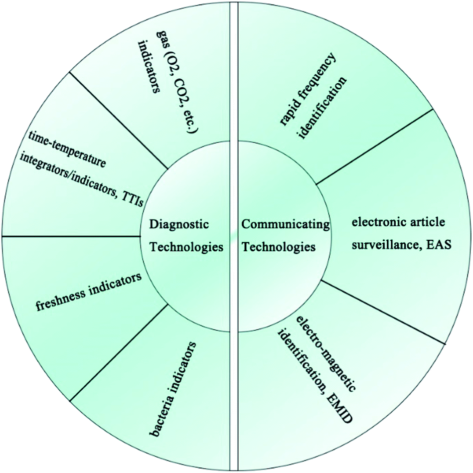 | ||
| Fig. 8 The main categories of IFP technologies. | ||
3.1 Diagnostic technologies in IFP using PE
In the diagnostic technologies, printed sensors are usually used as indicators to detect the inner environment of the food packaging.1–4,93 Printed sensors offer potential to improve efficiency without expensive equipment, and have been studied in lots of research. However, there are still some obstacles to be overcome: the sensors must be lightweight and flexible, production costs need to be decreased, sensitivity needs to be increased and the sensors must be eco-friendly.102Flexible printed sensors for food monitoring are complex integrated systems, which are typically composed of: (1) conducting electrodes based on conductive ink, (2) flexible/stretchable substrates, such as PI, PET, PEN, and (3) sensing materials. Fig. 9 shows the diagram of a flexible gas sensor in an IFP system. The sensing materials can monitor the environment inside of the package. The chemical signal can be changed into an electrical one by an electrode printed with effective conductive ink. The following section presents several flexible sensors that can be applied to IFP.
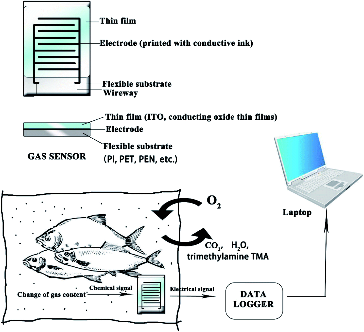 | ||
| Fig. 9 A diagram of an IFP system based on gas sensors. | ||
| Type of food | O2 (%) | CO2 (%) | N2 (%) |
|---|---|---|---|
| Red meat | 60–85 | 15–40 | — |
| Cooked meat/bacon | — | 20–35 | 65–80 |
| Poultry | — | 25 | 75 |
| Lean fish | 40 | 30 | |
| Oily fish | — | 60 | 40 |
| Salmon | 60 | 20 | |
| Hard cheese | — | 100 | — |
| Soft cheese | — | 30 | 70 |
| Bread | — | 60–70 | 30–40 |
| Milk free cake | — | 60 | 40 |
| Dairy cake | — | — | 100 |
| Fresh spaghetti | — | — | 100 |
| Fruit and vegetables | 3–5 | 3–5 | 85–95 |
Gas sensors are usually fabricated so that chemical reactions or changes in acidity lead to physical changes, for example, a change in resistance.108 They are crucial for controlling and recording changes in gas content and contribute to the extension of product shelf life. For example, Vargas-Sansalvador et al.109 reported the development of a water-based ionic liquid CO2 sensor which can be printed on food packaging. The sensor had an excellent optical performance and was especially sensitive to low concentrations of CO2. Lang and Jedermann110 demonstrated the detection of gas content in packaging for various gases such as O2, CO2, alcohols and so on. S. Santoro et al.111 prepared an O2 sensor based on the immobilization of tris-1,10-phenanthroline ruthenium which was printed onto a food packaging material to monitor oxygen permeation. This kind of sensor could also be used as a leakage indicator. Papadopoulou112 obtained a highly sensitive ammonia (NH3) gas sensor for food packaging technology based on pyromellitic dianhydride-4,4-oxydianiline, as shown in Fig. 10. When an NH3-releasing solution is injected into the package, the signal indicator of the sensor changes from blue to red. As the freshness of meat is closely related to the change of NH3 content in the packaging, this sensor would provide a technology for a real-time display of freshness of packaged meat.
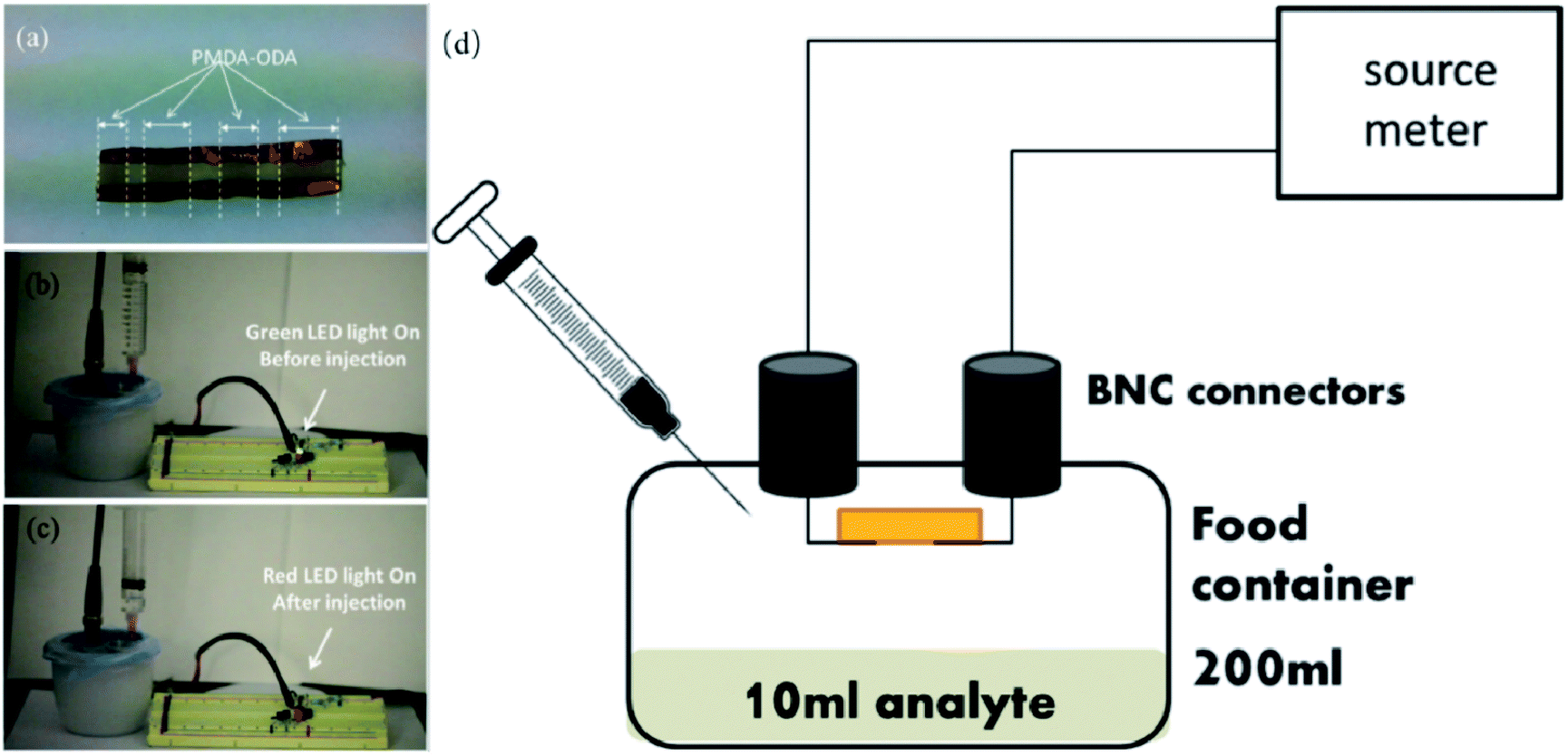 | ||
| Fig. 10 An NH3 sensor based on pyromellitic dianhydride-4,4-oxydianiline. (a) The darker parts of cotton is the cured polymer. (b) Before injection of NH3 solution the green led is on. (c) After the injection of NH3 solution the red led turns on. (d) Schematic representation of the experimenting set-up [adapted from ref. 112, E. L. Papadopoulou, D. Morselli, M. Prato, A. Barcellona, A. Athanassiou and I. S. Bayer, An efficient pure polyimide ammonia sensor, Journal of Materials Chemistry C, 2016, 4, 7790–7797. Copyright© Royal Society of Chemistry]. | ||
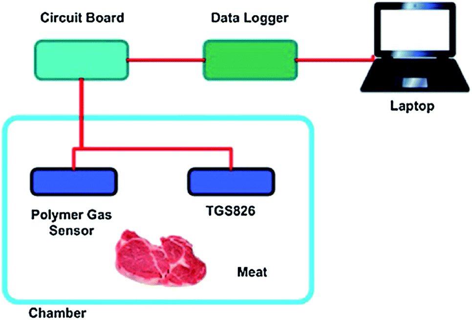 | ||
| Fig. 11 A schematic representation of an IFP system for monitoring NH3 gas in a chamber [reprinted with permission from ref. 121, S. Matindoust, A. Farzi, M. Baghaei Nejad, M. H. Shahrokh Abadi, Z. Zou and L.-R. Zheng, Ammonia gas sensor based on flexible polyaniline films for rapid detection of spoilage in protein-rich foods, Journal of Materials Science: Materials in Electronics, 2017, 28, 7760–7768. Copyright© Springer Nature]. | ||
Recently, biosensors have also been used to indicate freshness.122 Biosensors are made up of biological components (enzymes,123 antibodies124 and cells) and physical components that can decode the biological signal and change it to a physical one.125 Yang et al. presented some different CNT-based biosensors.126 For example, enzyme CNT-based biosensors were mentioned in their review. The large specific surface area of CNTs promotes enzyme conjugation so that such sensors can detect glucose and protein by bioreaction. A kind of highly efficient biosensor for glucose detection based on ZnO/ZnS core/shell nanotube arrays (CSNAs) was fabricated by Tarish et al.127 They demonstrated a method in which their ZnO/ZnS CSNA electrode gave a higher sensing performance than other reported sensors.
3.2 Communicating technologies in IFP using PEs
RFID technologies are unlike sensors and indicators and fall into another category. RFID tags contain transponders and antennas, satisfying the need of consumers for transparency in the supply chain and providing necessary and effective data for the production and sales decision-makers.4,101,128,129 Direct inkjet printing of antennas on plastic and paper substrates with the use of conductive NP inks is a promising approach to the production of low-cost RFID tags. RFID tags have broad application prospects for the following reasons: (i) they offer a large storage capacity (one to thousands of bytes); (ii) their readable distance through a scanner has a wide range (from a few centimeters to about two hundred meters); (iii) they can be operated without contact, and no particular angle is needed to read information; (iv) they are readable in diverse conditions (even in the dark or under water); and (v) they are recyclable.129,130 However, the biggest disadvantage of RFID is its cost, which is a stumbling block to wide-spread commercialization. Using RFID tags in IFP, the link of the supply chain at which the food begins to corrupt can be identified and RFID can speed customer checkout by recognition technology. Recently, many companies have started to use this technology to build a bridge between supermarkets, suppliers and consumers. Suppliers label their goods with RFID tags and once the goods reach the store center of the supermarket, the product labels are immediately scanned and the ID numbers are stored. When customers buy commodities, the ID numbers are deleted from the list of shelf products.Recently more intelligent RFID tags have been developed, such as sensor-enabled RFID tags to provide information on humidity and temperature. Borgese et al.131 fabricated a novel chipless RFID humidity sensor by inkjet printing. Variations in the relative humidity level from 50% to 90% gave a frequency shift of up to 270 MHz. It was based on a finite artificial impedance surface. Lorite et al.129 presented an RFID-assisted critical temperature indicator for supply chain monitoring using R2R printing. When the critical temperature that was detrimental to food storage was reached, the resistance rapidly increased (from 1 kΩ to 8 kΩ).
4. Outlook
PE offers wide application prospects in IFP as discussed. However, there are still some challenges and problems to be solved. The following goals remain: (i) decreasing the cost; (ii) simplifying production processes and increasing throughput; (iii) further diversifying applications in IFP; and (iv) developing eco-friendly raw materials with better properties.Conductive ink plays a crucial role in PE. Optimizing the properties of conductive ink is still a driving force in many literature reports. Nowadays, high-cost Ag ink is still universal in commercially available ink. Therefore, many researchers are focusing on developing low-cost alternative Cu, Al, and Ni nanomaterials with better properties. However, these types of nanomaterials are easily oxidized, causing deterioration of conductivity so researchers are searching for effective methods to stabilize these nanomaterials against oxidation. The addition of stabilizers is one common approach being considered; a second recent approach is to hinder oxidation of the NPs by, for example, synthesizing NPs with a dense shell that gives them antioxidant properties. Sintering is a key process for improving conductivity. Researchers are developing new sintering methods that avoid destruction of plastic or flexible substrates. For example, low temperature sintering has been studied recently. Low-cost carbonaceous materials are always considered as good candidates for metal-based conductive inks. However, their lower conductivity compared to that of metal NPs is a drawback. Some researchers still consider carbonaceous materials to offer the most prospects because many literature reports describe effective methods to improve their conductivity.
It should be noted that PE integrated with IFP has recently led to more effective functions to protect products. Various sensors for monitoring the changes in food and the inner environment of food packaging have been fabricated. RFID tags satisfy the present market, offering supply chain transparency and providing more information to retailers and manufacturers. However, the cost of RFID is indeed a big obstacle for further application. Developing lower-cost RFID tags with long service lives compatible with the shelf lives of products is still a burning issue. The application of RFID tags could be expanded for example through sensor-enabled RFID tags.
One more important application of PE is in flexible batteries and IFP displays. Nowadays, small volume batteries printed on flexible substrates as capacitors for high energy storage density together with flexible displays have been used to diversify packaging functions.
In this review, we have discussed issues from conductive ink synthesis to PE application to IFP, with the help of some reported articles. We trust that this review may help readers to better understand the preparation of conductive inks and the application of PE to IFP.
Conflicts of interest
The authors declare that they have no conflicts of interest.Acknowledgements
The authors gratefully acknowledge the financial support offered by the National Natural Science Foundation of China (Grant No. 51371129 and 1114226).References
- A. R. De Jong, H. Boumans, T. Slaghek, J. Van Veen, R. Rijk and M. Van Zandvoort, Active and intelligent packaging for food: is it the future?, Food Addit. Contam., 2005, 22, 975–979 CrossRef CAS PubMed.
- J. P. Kerry, M. N. O'Grady and S. A. Hogan, Past, current and potential utilisation of active and intelligent packaging systems for meat and muscle-based products: a review, Meat Sci., 2006, 74, 113–130 CrossRef CAS PubMed.
- C. E. Realini and B. Marcos, Active and intelligent packaging systems for a modern society, Meat Sci., 2014, 98, 404–419 CrossRef PubMed.
- N. Bumbudsanpharoke and S. Ko, Nanomaterial-based optical indicators: promise, opportunities, and challenges in the development of colorimetric systems for intelligent packaging, Nano Res., 2018, 12, 489–500 CrossRef.
- X. Dai, W. Xu, T. Zhang, H. Shi and T. Wang, Room temperature sintering of Cu-Ag core-shell nanoparticles conductive inks for printed electronics, Chem. Eng. J., 2019, 364, 310–319 CrossRef CAS.
- A. Kamyshny and S. Magdassi, Conductive Nanomaterials for Printed Electronics, Small, 2014, 10, 3515–3535 CrossRef CAS PubMed.
- A. Kamyshny and S. Magdassi, Conductive nanomaterials for 2D and 3D printed flexible electronics, Chem. Soc. Rev., 2019, 48, 1712–1740 RSC.
- L. He and S. C. Tjong, Nanostructured transparent conductive films: fabrication, characterization and applications, Mater. Sci. Eng., R, 2016, 109, 1–101 CrossRef.
- W. Yang and C. Wang, Graphene and the related conductive inks for flexible electronics, J. Mater. Chem. C, 2016, 4, 7193–7207 RSC.
- B. Tian, W. Yao, P. Zeng, X. Li, H. Wang, L. Liu, Y. Feng, C. Luo and W. Wu, All-printed, low-cost, tunable sensing range strain sensors based on Ag nanodendrite conductive inks for wearable electronics, J. Mater. Chem. C, 2019, 7, 809–818 RSC.
- G. Mattana, A. Loi, M. Woytasik, M. Barbaro, V. Noël and B. Piro, Inkjet-Printing: A New Fabrication Technology for Organic Transistors, Adv. Mater. Technol., 2017, 2 CAS.
- W. Wu, Inorganic nanomaterials for printed electronics: a review, Nanoscale, 2017, 9, 7342–7372 RSC.
- Y. Liao, R. Zhang, H. Wang, S. Ye, Y. Zhou, T. Ma, J. Zhu, L. D. Pfefferle and J. Qian, Highly conductive carbon-based aqueous inks toward electroluminescent devices, printed capacitive sensors and flexible wearable electronics, RSC Adv., 2019, 9, 15184–15189 RSC.
- G. Cummins and M. P. Y. Desmulliez, Inkjet printing of conductive materials: a review, Circuit World, 2012, 38, 193–213 CrossRef CAS.
- H. J. Gysling, Nanoinks in inkjet metallization — Evolution of simple additive-type metal patterning, Curr. Opin. Colloid Interface Sci., 2014, 19, 155–162 CrossRef CAS.
- S. I. Na, Y. H. Seo, Y. C. Nah, S. S. Kim, H. Heo, J. E. Kim, N. Rolston, R. H. Dauskardt, M. Gao, Y. Lee and D. Vak, High Performance Roll-to-Roll Produced Fullerene-Free Organic Photovoltaic Devices via Temperature-Controlled Slot Die Coating, Adv. Funct. Mater., 2018, 29 Search PubMed.
- S. Barui, S. Mandal and B. Basu, Thermal inkjet 3D powder printing of metals and alloys: current status and challenges, Current Opinion in Biomedical Engineering, 2017, 2, 116–123 CrossRef.
- Z. Chu, J. Peng and W. Jin, Advanced nanomaterial inks for screen-printed chemical sensors, Sens. Actuators, B, 2017, 243, 919–926 CrossRef CAS.
- W. Li, X. Xu, W. Li, Y. Zhao and M. Chen, Green synthesis of micron-sized silver flakes and their application in conductive ink, J. Mater. Sci., 2018, 53, 6424–6432 CrossRef CAS.
- L. Mo, Z. Guo, L. Yang, Q. Zhang, Y. Fang, Z. Xin, Z. Chen, K. Hu, L. Han and L. Li, Silver Nanoparticles Based Ink with Moderate Sintering in Flexible and Printed Electronics, Int. J. Mol. Sci., 2019, 20 CAS.
- Y. Li, M. Roundhill, M. Yang, I. Pavlovsky, R. L. Fink and Z. Yaniv, Photo-curing process for metallic inks, US Pat., US20090311440A1, Aug. 8, 2017.
- M. Layani, A. Kamyshny and S. Magdassi, Transparent conductors composed of nanomaterials, Nanoscale, 2014, 6, 5581–5591 RSC.
- L. Polavarapu, K. K. Manga, H. D. Cao, K. P. Loh and Q.-H. Xu, Preparation of Conductive Silver Films at Mild Temperatures for Printable Organic Electronics, Chem. Mater., 2011, 23, 3273–3276 CrossRef CAS.
- L. Polavarapu, K. K. Manga, K. Yu, P. K. Ang, H. D. Cao, J. Balapanuru, K. P. Loh and Q. H. Xu, Alkylamine capped metal nanoparticle “inks” for printable SERS substrates, electronics and broadband photodetectors, Nanoscale, 2011, 3, 2268–2274 RSC.
- Y. Wang, X. Li, J. Luo, J. Zhang, W. Jianjun and Y. Tang, Fabrication of Ag nanocluster and adjustment of particle size by plasma vapor deposition, High Power Laser Part. Beams, 2014, 26(08), 26082001 Search PubMed.
- K. Gerasopoulos, E. Pomerantseva, M. McCarthy, A. Brown, C. Wang, J. Culver and R. Ghodssi, Hierarchical three-dimensional microbattery electrodes combining bottom-up self-assembly and top-down micromachining, ACS Nano, 2012, 6, 6422–6432 CrossRef CAS PubMed.
- F. Hoeng, J. Bras, E. Gicquel, G. Krosnicki and A. Denneulin, Inkjet printing of nanocellulose–silver ink onto nanocellulose coated cardboard, RSC Adv., 2017, 7, 15372–15381 RSC.
- S. S. Narwade, B. B. Mulik, S. M. Mali and B. R. Sathe, Silver nanoparticles sensitized C60(Ag@C60) as efficient electrocatalysts for hydrazine oxidation: implication for hydrogen generation reaction, Appl. Surf. Sci., 2017, 396, 939–944 CrossRef CAS.
- A. Pajor-Świerzy, Y. Farraj, A. Kamyshny and S. Magdassi, Effect of carboxylic acids on conductivity of metallic films formed by inks based on copper@silver core-shell particles, Colloids Surf., A, 2017, 522, 320–327 CrossRef.
- K. Ranoszek-Soliwoda, E. Tomaszewska, E. Socha, P. Krzyczmonik, A. Ignaczak, P. Orlowski, M. Krzyzowska, G. Celichowski and J. Grobelny, The role of tannic acid and sodium citrate in the synthesis of silver nanoparticles, J. Nanopart. Res., 2017, 19, 273 CrossRef PubMed.
- T. Jayaramudu, G. M. Raghavendra, K. Varaprasad, G. V. S. Reddy, A. B. Reddy, K. Sudhakar and E. R. Sadiku, Preparation and characterization of poly(ethylene glycol) stabilized nano silver particles by a mechanochemical assisted ball mill process, J. Appl. Polym. Sci., 2016, 133 CrossRef.
- K. Afshinnia, M. Sikder, B. Cai and M. Baalousha, Effect of nanomaterial and media physicochemical properties on Ag NM aggregation kinetics, J. Colloid Interface Sci., 2017, 487, 192–200 CrossRef CAS PubMed.
- S. Mu, W. Liu, L. Zhao, Y. Long and H. Gu, Antimicrobial AgNPs composites of gelatin hydrogels crosslinked by ferrocene-containing tetrablock terpolymer, Polymer, 2019, 169, 80–94 CrossRef CAS.
- G. V. Kurlyandskaya, I. P. Novoselova, V. V. Schupletsova, R. Andrade, N. A. Dunec, L. S. Litvinova, A. P. Safronov, K. A. Yurova, N. A. Kulesh, A. N. Dzyuman and I. A. Khlusov, Nanoparticles for magnetic biosensing systems, J. Magn. Magn. Mater., 2017, 431, 249–254 CrossRef CAS.
- S. M. Louie, J. M. Gorham, J. Tan and V. A. Hackley, Ultraviolet photo-oxidation of polyvinylpyrrolidone (PVP) coatings on gold nanoparticles, Environ. Sci.: Nano, 2017, 4 RSC.
- M. Yu, Y. Han, J. Li and L. Wang, One-step synthesis of sodium carboxymethyl cellulose-derived carbon aerogel/nickel oxide composites for energy storage, Chem. Eng. J., 2017, 324, 287–295 CrossRef CAS.
- C. Joanna, L. Marcin, K. Ewa and P. Grazyna, A nonspecific synergistic effect of biogenic silver nanoparticles and biosurfactant towards environmental bacteria and fungi, Ecotoxicology, 2018, 27, 352–359 CrossRef CAS PubMed.
- M. Seo, J. S. Kim, J. G. Lee, S. B. Kim and S. M. Koo, The effect of silver particle size and organic stabilizers on the conductivity of silver particulate films in thermal sintering processes, Thin Solid Films, 2016, 616, 366–374 CrossRef CAS.
- C. Cheng, J. Li, T. Shi, X. Yu, J. Fan, G. Liao, X. Li, S. Cheng, Y. Zhong and Z. Tang, A novel method of synthesizing antioxidative copper nanoparticles for high performance conductive ink, J. Mater. Sci.: Mater. Electron., 2017, 28, 13556–13564 CrossRef CAS.
- C. Yim, Z. A. Kockerbeck, S. B. Jo and S. S. Park, Hybrid Copper-Silver-Graphene Nanoplatelet Conductive Inks on PDMS for Oxidation Resistance Under Intensive Pulsed Light, ACS Appl. Mater. Interfaces, 2017, 9, 37160–37165 CrossRef CAS PubMed.
- A. Pajor-Świerzy, Y. Farraj, A. Kamyshny and S. Magdassi, Air stable copper-silver core-shell submicron particles: Synthesis and conductive ink formulation, Colloids Surf., A, 2017, 521, 272–280 CrossRef.
- M. Krivec, A. Roshanghias, A. Abram and A. Binder, Exploiting the combination of 3D polymer printing and inkjet Ag-nanoparticle printing for advanced packaging, Microelectron. Eng., 2017, 176, 1–5 CrossRef CAS.
- H. M. Cronin, Z. Stoeva, M. Brown, M. Shkunov and S. R. P. Silva, Photonic Curing of Low-Cost Aqueous Silver Flake Inks for Printed Conductors with Increased Yield, ACS Appl. Mater. Interfaces, 2018, 10, 21398–21410 CrossRef CAS PubMed.
- Y.-T. Kwon, Y.-I. Lee, S. Kim, K.-J. Lee and Y.-H. Choa, Full densification of inkjet-printed copper conductive tracks on a flexible substrate utilizing a hydrogen plasma sintering, Appl. Surf. Sci., 2017, 396, 1239–1244 CrossRef CAS.
- C. Ayyappadas, A. Muthuchamy, A. Raja Annamalai and D. K. Agrawal, An investigation on the effect of sintering mode on various properties of copper-graphene metal matrix composite, Adv. Powder Technol., 2017, 28, 1760–1768 CrossRef CAS.
- H. Koga, T. Inui, I. Miyamoto, T. Sekiguchi, M. Nogi and K. Suganuma, A high-sensitivity printed antenna prepared by rapid low-temperature sintering of silver ink, RSC Adv., 2016, 6, 84363–84368 RSC.
- D. Kim and J. Moon, Highly Conductive Ink Jet Printed Films of Nanosilver Particles for Printable Electronics, Electrochem. Solid-State Lett., 2005, 8, 30–33 CrossRef.
- S. Magdassi, M. Grouchko, O. Berezin and K. Alexander, Triggering the Sintering of Silver Nanoparticles at Room Temperature, ACS Nano, 2010, 4, 1943–1948 CrossRef CAS PubMed.
- A. Maattanen, P. Ihalainen, P. Pulkkinen, S. Wang, H. Tenhu and J. Peltonen, Inkjet-printed gold electrodes on paper: characterization and functionalization, ACS Appl. Mater. Interfaces, 2012, 4, 955–964 CrossRef PubMed.
- Y. Mou, Y. Zhang, H. Cheng, Y. Peng and M. Chen, Fabrication of highly conductive and flexible printed electronics by low temperature sintering reactive silver ink, Appl. Surf. Sci., 2018, 459, 249–256 CrossRef CAS.
- Y. T. Kwon, Y. S. Kim, Y. Lee, S. Kwon, M. Lim, Y. Song, Y. H. Choa and W. H. Yeo, Ultrahigh Conductivity and Superior Interfacial Adhesion of a Nanostructured, Photonic-Sintered Copper Membrane for Printed Flexible Hybrid Electronics, ACS Appl. Mater. Interfaces, 2018, 10, 44071–44079 CrossRef CAS PubMed.
- Y. K. Lee, J. Kim, Y. Kim, J. W. Kwak, Y. Yoon and J. A. Rogers, Room Temperature Electrochemical Sintering of Zn Microparticles and Its Use in Printable Conducting Inks for Bioresorbable Electronics, Adv. Mater., 2017, 29 Search PubMed.
- S.-H. Park and H.-S. Kim, Flash light sintering of nickel nanoparticles for printed electronics, Thin Solid Films, 2014, 550, 575–581 CrossRef CAS.
- J.-H. Chu, S.-J. Joo and H.-S. Kim, Development of a via-hole connection process via intense pulsed light sintering with Cu micro/Ag nano-hybrid ink for a multi-layered flexible printed circuit board, Thin Solid Films, 2019, 680, 1–11 CrossRef CAS.
- C. Tang, H.-F. Wang, J.-Q. Huang, W. Qian, F. Wei, S.-Z. Qiao and Q. Zhang, 3D Hierarchical Porous Graphene-Based Energy Materials: Synthesis, Functionalization, and Application in Energy Storage and Conversion, Electrochemical Energy Reviews, 2019, 2, 332–371 CrossRef CAS.
- E. Yakimchuk, R. Soots, I. Kotin and I. Antonova, 2D printed graphene conductive layers with high carrier mobility, Current Applied Physics, 2017, 17, 1655–1661 CrossRef.
- J. Phiri, P. Gane and T. C. Maloney, General overview of graphene: production, properties and application in polymer composites, Mater. Sci. Eng., B, 2017, 215, 9–28 CrossRef CAS.
- A. K. Geim and K. S. Novoselov, The rise of graphene, Manchester Centre for Mesoscience and Nanotechnology, University of Manchester, Oxford Road M13 9PL, United Kingdom, 2009 Search PubMed.
- M. L. Yola, Development of Novel Nanocomposites Based on Graphene/Graphene Oxide and Electrochemical Sensor Applications, Curr. Anal. Chem., 2019, 15, 159–165 CrossRef CAS.
- H. Hibino, S. Wang, C. M. Orofeo and H. Kageshima, Growth and low-energy electron microscopy characterizations of graphene and hexagonal boron nitride, Prog. Cryst. Growth Charact. Mater., 2016, 62, 155–176 CrossRef CAS.
- H. Zheng, Y. Gan, P. Abbamonte and L. K. Wagner, Importance of sigma Bonding Electrons for the Accurate Description of Electron Correlation in Graphene, Phys. Rev. Lett., 2017, 119, 166402 CrossRef PubMed.
- P. G. Karagiannidis, S. A. Hodge, L. Lombardi, F. Tomarchio, N. Decorde, S. Milana, I. Goykhman, Y. Su, S. V. Mesite, D. N. Johnstone, R. K. Leary, P. A. Midgley, N. M. Pugno, F. Torrisi and A. C. Ferrari, Microfluidization of Graphite and Formulation of Graphene-Based Conductive Inks, ACS Nano, 2017, 11, 2742–2755 CrossRef CAS PubMed.
- J. Li, H. Yan, D. Dang, W. Wei and L. Meng, Salt and water co-assisted exfoliation of graphite in organic solvent for efficient and large scale production of high-quality graphene, J. Colloid Interface Sci., 2019, 535, 92–99 CrossRef CAS PubMed.
- B. H. Nguyen and V. H. Nguyen, Promising applications of graphene and graphene-based nanostructures, Adv. Nat. Sci.: Nanosci. Nanotechnol., 2016, 7 Search PubMed.
- M. Yi and Z. Shen, Fluid dynamics: an emerging route for the scalable production of graphene in the last five years, RSC Adv., 2016, 6, 72525–72536 RSC.
- S. N. Alam, N. Sharma and L. Kumar, Synthesis of Graphene Oxide (GO) by Modified Hummers Method and Its Thermal Reduction to Obtain Reduced Graphene Oxide (rGO)*, Graphene, 2017, 06, 1–18 CrossRef CAS.
- O. Jankovsky, M. Novacek, J. Luxa, D. Sedmidubsky, M. Bohacova, M. Pumera and Z. Sofer, Concentration of Nitric Acid Strongly Influences Chemical Composition of Graphite Oxide, Chemistry, 2017, 23, 6432–6440 CrossRef CAS PubMed.
- Y. Z. Wang, T. Chen, H. H. Liu, X. C. Wang and X. X. Zhang, Direct Liquid Phase Exfoliation of Graphite to Produce Few-Layer Graphene by Microfluidization, J. Nanosci. Nanotechnol., 2019, 19, 2078–2086 CrossRef CAS PubMed.
- L. Huang, J. Pei, H. Jiang, C. Li and X. Hu, Electricity generation across graphene oxide membranes, Mater. Res. Bull., 2018, 97, 96–100 CrossRef CAS.
- M. L. Ould Ne, M. Boujnah, A. Benyoussef and A. E. Kenz, Electronic and Electrical Conductivity of AB and AA-Stacked Bilayer Graphene with Tunable Layer Separation, J. Supercond. Novel Magn., 2016, 30, 1263–1267 CrossRef.
- A. Ebdam, S. Jameh-Bozorghi, M. Yousefi and A. Niazi, Enhanced fire retardancy of polyvinylchloride by combination with graphene and magnesium hydroxide, Bulg. Chem. Commun., 2017, 152–158 Search PubMed , Special Issue J.
- K. Beltrop, S. Beuker, A. Heckmann, M. Winter and T. Placke, Alternative electrochemical energy storage: potassium-based dual-graphite batteries, Energy Environ. Sci., 2017, 10, 2090–2094 RSC.
- J. Tian, L. Guo, X. Yin and W. Wu, The liquid-phase preparation of graphene by shear exfoliation with graphite oxide as a dispersant, Mater. Chem. Phys., 2019, 223, 1–8 CrossRef CAS.
- H. Shuai, Graphene Ink Fabricated Screen Printed Electrode for Cd2+ and Pd2+ Determination in Xiangjiang River, Int. J. Electrochem. Sci., 2016, 7430–7439, DOI:10.20964/2016.09.387.
- W. Ren and H. M. Cheng, The global growth of graphene, Nat. Nanotechnol., 2014, 9, 726–730 CrossRef CAS PubMed.
- H. Gao, K. Zhu, G. Hu and C. Xue, Large-scale graphene production by ultrasound-assisted exfoliation of natural graphite in supercritical CO2/H2O medium, Chem. Eng. J., 2017, 308, 872–879 CrossRef CAS.
- D. Dodoo-Arhin, R. C. T. Howe, G. Hu, Y. Zhang, P. Hiralal, A. Bello, G. Amaratunga and T. Hasan, Inkjet-printed graphene electrodes for dye-sensitized solar cells, Carbon, 2016, 105, 33–41 CrossRef CAS.
- A. O. Osikoya, O. Parlak, N. A. Murugan, E. D. Dikio, H. Moloto, L. Uzun, A. P. F. Turner and A. Tiwari, Acetylene-sourced CVD-synthesised catalytically active graphene for electrochemical biosensing, Biosens. Bioelectron., 2017, 89, 496–504 CrossRef CAS PubMed.
- K. Thodkar, D. Thompson, F. Luond, L. Moser, F. Overney, L. Marot, C. Schonenberger, B. Jeanneret and M. Calame, Restoring the Electrical Properties of CVD Graphene via Physisorption of Molecular Adsorbates, ACS Appl. Mater. Interfaces, 2017, 9, 25014–25022 CrossRef CAS PubMed.
- Y. Liu, B. Sun, J. Li, D. Cheng, X. An, B. Yang, Z. He, R. Lutes, A. Khan and Y. Ni, Aqueous Dispersion of Carbon Fibers and Expanded Graphite Stabilized from the Addition of Cellulose Nanocrystals to Produce Highly Conductive Cellulose Composites, ACS Sustainable Chem. Eng., 2018, 6, 3291–3298 CrossRef CAS.
- L. Shao, H. Wang, Y. Yang, Y. He, Y. Tang, H. Fang, J. Zhao, H. Xiao, K. Liang, M. Wei, W. Xu, M. Luo, Q. Wan, W. Hu, T. Gao and Z. Cui, Optoelectronic Properties of Printed Photogating Carbon Nanotube Thin Film Transistors and Their Application for Light-Stimulated Neuromorphic Devices, ACS Appl. Mater. Interfaces, 2019, 11, 12161–12169 CrossRef CAS PubMed.
- S. Kumar, M. Nehra, D. Kedia, N. Dilbaghi, K. Tankeshwar and K.-H. Kim, Carbon nanotubes: A potential material for energy conversion and storage, Prog. Energy Combust. Sci., 2018, 64, 219–253 CrossRef.
- S. R. Shin, R. Farzad, A. Tamayol, V. Manoharan, P. Mostafalu, Y. S. Zhang, M. Akbari, S. M. Jung, D. Kim, M. Comotto, N. Annabi, F. E. Al-Hazmi, M. R. Dokmeci and A. Khademhosseini, A Bioactive Carbon Nanotube-Based Ink for Printing 2D and 3D Flexible Electronics, Adv. Mater., 2016, 28, 3280–3289 CrossRef CAS PubMed.
- B. Wang, R. Jiang, W. Song and H. Liu, Controlling dispersion of graphene nanoplatelets in aqueous solution by ultrasonic technique, Russ. J. Phys. Chem. A, 2017, 91, 1517–1526 CrossRef CAS.
- W. Zhao, F. Wu, H. Wu and G. Chen, Preparation of Colloidal Dispersions of Graphene Sheets in Organic Solvents by Using Ball Milling, J. Nanomater., 2010, 2010, 1–5 Search PubMed.
- S. Kim, B. Tserengombo, S.-H. Choi, J. Noh, S. Huh, B. Choi, H. Chung, J. Kim and H. Jeong, Experimental investigation of dispersion characteristics and thermal conductivity of various surfactants on carbon based nanomaterial, Int. Commun. Heat Mass Transfer, 2018, 91, 95–102 CrossRef CAS.
- D. Song, A. Mahajan, E. B. Secor, M. C. Hersam, L. F. Francis and C. D. Frisbie, High-Resolution Transfer Printing of Graphene Lines for Fully Printed, Flexible Electronics, ACS Nano, 2017, 11, 7431–7439 CrossRef CAS PubMed.
- E. B. Secor, P. L. Prabhumirashi, K. Puntambekar, M. L. Geier and M. C. Hersam, Inkjet Printing of High Conductivity, Flexible Graphene Patterns, J. Phys. Chem. Lett., 2013, 4, 1347–1351 CrossRef CAS PubMed.
- C.-L. Lee, C.-H. Chen and C.-W. Chen, Graphene nanosheets as ink particles for inkjet printing on flexible board, Chem. Eng. J., 2013, 230, 296–302 CrossRef CAS.
- M. Michel, C. Biswas and A. B. Kaul, High-performance ink-jet printed graphene resistors formed with environmentally-friendly surfactant-free inks for extreme thermal environments, Applied Materials Today, 2017, 6, 16–21 CrossRef.
- A. Koutsioukis, V. Georgakilas, V. Belessi and R. Zboril, Highly Conductive Water-Based Polymer/Graphene Nanocomposites for Printed Electronics, Chemistry, 2017, 23, 8268–8274 CrossRef CAS PubMed.
- M. H. Overgaard, M. Kühnel, R. Hvidsten, S. V. Petersen, T. Vosch, K. Nørgaard and B. W. Laursen, Highly Conductive Semitransparent Graphene Circuits Screen-Printed from Water-Based Graphene Oxide Ink, Adv. Mater. Technol., 2017, 2 CAS.
- S. Majee, C. Liu, B. Wu, S. L. Zhang and Z. B. Zhang, Ink-jet printed highly conductive pristine graphene patterns achieved with water-based ink and aqueous doping processing, Carbon, 2017, 114, 77–83 CrossRef CAS.
- K. Parvez, Z. S. Wu, R. Li, X. Liu, R. Graf, X. Feng and K. Mullen, Exfoliation of graphite into graphene in aqueous solutions of inorganic salts, J. Am. Chem. Soc., 2014, 136, 6083–6091 CrossRef CAS PubMed.
- A. Al Shboul, C. Trudeau, S. Cloutier, M. Siaj and J. P. Claverie, Graphene dispersions in alkanes: toward fast drying conducting inks, Nanoscale, 2017, 9, 9893–9901 RSC.
- S. Man, Graphene Based Inks for Printed Electronics, Uppsala University, SE-75121 Uppsala, Sweden, 2019 Search PubMed.
- Y. Meng, X.-B. Xu, H. Li, Y. Wang, E.-X. Ding, Z.-C. Zhang and H.-Z. Geng, Optimisation of carbon nanotube ink for large-area transparent conducting films fabricated by controllable rod-coating method, Carbon, 2014, 70, 103–110 CrossRef CAS.
- C. Preston, D. Song, J. Dai, Z. Tsinas, J. Bavier, J. Cumings, V. Ballarotto and L. Hu, Scalable nanomanufacturing of surfactant-free carbon nanotube inks for spray coatings with high conductivity, Nano Res., 2015, 8, 2242–2250 CrossRef CAS.
- S. Wang, N. Liu, J. Tao, C. Yang, W. Liu, Y. Shi, Y. Wang, J. Su, L. Li and Y. Gao, Inkjet printing of conductive patterns and supercapacitors using a multi-walled carbon nanotube/Ag nanoparticle based ink, J. Mater. Chem. A, 2015, 3, 2407–2413 RSC.
- S. Azoz, A. L. Exarhos, A. Marquez, L. M. Gilbertson, S. Nejati, J. J. Cha, J. B. Zimmerman, J. M. Kikkawa and L. D. Pfefferle, Highly conductive single-walled carbon nanotube thin film preparation by direct alignment on substrates from water dispersions, Langmuir, 2015, 31, 1155–1163 CrossRef CAS PubMed.
- D. Dainelli, N. Gontard, D. Spyropoulos, E. Zondervan-van den Beuken and P. Tobback, Active and intelligent food packaging: legal aspects and safety concerns, Trends Food Sci. Technol., 2008, 19, S103–S112 CrossRef.
- S. Y. Tseng, S. Y. Li, S. Y. Yi, A. Y. Sun, D. Y. Gao and D. Wan, Food Quality Monitor: Paper-Based Plasmonic Sensors Prepared Through Reversal Nanoimprinting for Rapid Detection of Biogenic Amine Odorants, ACS Appl. Mater. Interfaces, 2017, 9, 17306–17316 CrossRef CAS PubMed.
- S. J. Calva-Estrada, M. Jiménez-Fernández and E. Lugo-Cervantes, Protein-Based Films: Advances in the Development of Biomaterials Applicable to Food Packaging, Food Eng. Rev., 2019, 11, 78–92 CrossRef CAS.
- C. Moreno, M. J. Andrade-Cuvi, M. J. Zaro, M. Darre, A. R. Vicente and A. Concellón, Short UV-C Treatment Prevents Browning and Extends the Shelf-Life of Fresh-Cut Carambola, J. Food Qual., 2017, 2017, 1–9 CrossRef.
- S. Yildirim, B. Röcker, M. K. Pettersen, J. Nilsen-Nygaard, Z. Ayhan, R. Rutkaite, T. Radusin, P. Suminska, B. Marcos and V. Coma, Active Packaging Applications for Food, Compr. Rev. Food Sci. Food Saf., 2018, 17, 165–199 CrossRef PubMed.
- P. Puligundla, J. Jung and S. Ko, Carbon dioxide sensors for intelligent food packaging applications, Food Control, 2012, 25, 328–333 CrossRef CAS.
- M. D. Wilson, R. A. Stanley, A. Eyles and T. Ross, Innovative processes and technologies for modified atmosphere packaging of fresh and fresh-cut fruits and vegetables, Crit. Rev. Food Sci. Nutr., 2019, 59, 411–422 CrossRef CAS PubMed.
- F. Bibi, C. Guillaume, N. Gontard and B. Sorli, Wheat gluten, a bio-polymer to monitor carbon dioxide in food packaging: electric and dielectric characterization, Sens. Actuators, B, 2017, 250, 76–84 CrossRef CAS.
- I. M. Perez de Vargas-Sansalvador, M. M. Erenas, D. Diamond, B. Quilty and L. F. Capitan-Vallvey, Water based-ionic liquid carbon dioxide sensor for applications in the food industry, Sens. Actuators, B, 2017, 253, 302–309 CrossRef CAS.
- W. Lang and R. Jedermann, What Can MEMS Do for Logistics of Food? Intelligent Container Technologies: A Review, IEEE Sensors Journal, 2016, 16, 6810–6818 Search PubMed.
- S. Santoro, A. J. Moro, C. Portugal, J. G. Crespo, J. C. Lima and I. M. Coelhoso, Monitoring oxygen permeation through polymeric packaging films using a ratiometric luminescent sensor, J. Food Eng., 2016, 189, 37–44 CrossRef CAS.
- E. L. Papadopoulou, D. Morselli, M. Prato, A. Barcellona, A. Athanassiou and I. S. Bayer, An efficient pure polyimide ammonia sensor, J. Mater. Chem. C, 2016, 4, 7790–7797 RSC.
- C. A. Aceves Lara, V. Athès, P. Buche, G. Della Valle, V. Farines, F. Fonseca, V. Guillard, K. Kansou, M. Kristiawan, V. Monclus, J.-R. Mouret, A. Ndiaye, P. Neveu, S. Passot, C. Pénicaud, J.-M. Sablayrolles, J.-M. Salmon, R. Thomopoulos and I. C. Trelea, The virtual food system: Innovative models and experiential feedback in technologies for winemaking, the cereals chain, food packaging and eco-designed starter production, Innovative Food Sci. Emerging Technol., 2018, 46, 54–64 CrossRef.
- C. Alamprese, C. Cappa, S. Ratti, S. Limbo, M. Signorelli, D. Fessas and M. Lucisano, Shelf life extension of whole-wheat breadsticks: formulation and packaging strategies, Food Chem., 2017, 230, 532–539 CrossRef CAS PubMed.
- A. Paternoster, J. Van Camp, S. Vanlanduit, A. Weeren, J. Springael and J. Braet, The performance of beer packaging: vibration damping and thermal insulation, Food Packaging and Shelf Life, 2017, 11, 91–97 CrossRef.
- O. A. Odeyemi, C. M. Burke, C. J. S. Bolch and R. Stanley, Evaluation of spoilage potential and volatile metabolites production by Shewanella baltica isolated from modified atmosphere packaged live mussels, Food Res. Int., 2018, 103, 415–425 CrossRef CAS PubMed.
- E. Poyatos-Racionero, J. V. Ros-Lis, J.-L. Vivancos and R. Martínez-Máñez, Recent advances on intelligent packaging as tools to reduce food waste, J. Cleaner Prod., 2018, 172, 3398–3409 CrossRef.
- P. Kumar, S. K. Mohanty, S. Guruswamy, Y. R. Smith and M. Misra, Detection of Food Decay Products Using Functionalized One-Dimensional Titania Nanotubular Arrays, IEEE Sensors Letters, 2017, 1, 1–4 CAS.
- C. Schaude, C. Meindl, E. Frohlich, J. Attard and G. J. Mohr, Developing a sensor layer for the optical detection of amines during food spoilage, Talanta, 2017, 170, 481–487 CrossRef CAS PubMed.
- A. T. Alreshaid, J. G. Hester, W. Su, Y. Fang and M. M. Tentzeris, Review—Ink-Jet Printed Wireless Liquid and Gas Sensors for IoT, SmartAg and Smart City Applications, J. Electrochem. Soc., 2018, 165, B407–B413 CrossRef CAS.
- S. Matindoust, A. Farzi, M. Baghaei Nejad, M. H. Shahrokh Abadi, Z. Zou and L.-R. Zheng, Ammonia gas sensor based on flexible polyaniline films for rapid detection of spoilage in protein-rich foods, J. Mater. Sci.: Mater. Electron., 2017, 28, 7760–7768 CrossRef CAS.
- E. Omanovic-Miklicanin and S. Valzacchi, Development of new chemiluminescence biosensors for determination of biogenic amines in meat, Food Chem., 2017, 235, 98–103 CrossRef CAS PubMed.
- O. Gubanova, M. Andrianova, M. Saveliev, N. Komarova, E. Kuznetsov and A. Kuznetsov, Fabrication and package of ISFET biosensor for micro volume analysis with the use of direct ink writing approach, Mater. Sci. Semicond. Process., 2017, 60, 71–78 CrossRef CAS.
- F. Magesa, Y. Wu, Y. Tian, J.-M. Vianney, J. Buza, Q. He and Y. Tan, Graphene and graphene like 2D graphitic carbon nitride: electrochemical detection of food colorants and toxic substances in environment, Trends Environ. Anal. Chem., 2019, 23 CAS.
- W. Dudefoi, A. Villares, S. Peyron, C. Moreau, M.-H. Ropers, N. Gontard and B. Cathala, Nanoscience and nanotechnologies for biobased materials, packaging and food applications: new opportunities and concerns, Innovative Food Sci. Emerging Technol., 2018, 46, 107–121 CrossRef CAS.
- N. Yang, X. Chen, T. Ren, P. Zhang and D. Yang, Carbon nanotube based biosensors, Sens. Actuators, B, 2015, 207, 690–715 CrossRef CAS.
- S. Tarish, Y. Xu, Z. Wang, F. Mate, A. Al-Haddad, W. Wang and Y. Lei, Highly efficient biosensors by using well-ordered ZnO/ZnS core/shell nanotube arrays, Nanotechnology, 2017, 28, 405501 CrossRef PubMed.
- F. Bibi, C. Guillaume, N. Gontard and B. Sorli, A review: RFID technology having sensing aptitudes for food industry and their contribution to tracking and monitoring of food products, Trends Food Sci. Technol., 2017, 62, 91–103 CrossRef CAS.
- G. S. Lorite, T. Selkala, T. Sipola, J. Palenzuela, E. Jubete, A. Vinuales, G. Cabanero, H. J. Grande, J. Tuominen, S. Uusitalo, L. Hakalahti, K. Kordas and G. Toth, Novel, smart and RFID assisted critical temperature indicator for supply chain monitoring, J. Food Eng., 2017, 193, 20–28 CrossRef.
- M. Creydt and M. Fischer, Blockchain and more - Algorithm driven food traceability, Food Control, 2019, 105, 45–51 CrossRef CAS.
- M. Borgese and F. Costa, An Inkjet Printed Chipless RFID Sensor for Wireless Humidity Monitoring, IEEE Sensors Journal, 2017, 17, 5 Search PubMed.
| This journal is © The Royal Society of Chemistry 2019 |