
Graphene networks for high-performance flexible and transparent supercapacitors†
Xueliu Fan,
Tao Chen and
Liming Dai*
Center of Advanced Science and Engineering for Carbon (Case4Carbon) and Department of Macromolecular Science and Engineering, Case Western Reserve University, 10900 Euclid Avenue, Cleveland, Ohio 44106, USA. E-mail: liming.dai@case.edu
First published on 30th July 2014
Abstract
Graphene network (GN) was synthesized by a two-step chemical vapour deposition (CVD) method, involving the thermal annealing sputter-coated Cu film to form a Cu network by annealing for CVD deposition of graphene onto the Cu network catalyst. The resultant graphene network was transferred onto a flexible and transparent polymer (e.g., PDMS) substrate while maintaining its porous structure and integrated interconnection, providing both good optical transparency (e.g., transmittance of 86% at 550 nm wavelength) and mechanical flexibility. Flexible and transparent all-solid-state supercapacitors based on the newly-developed graphene network were fabricated to exhibit an area specific capacitance of 4.2 μF cm−2 at a discharge current of 0.1 μA with a high optical transparency (transmittance of 84%), which outperforms devices based on uniform multi-layer graphene sheet.
1. Introduction
As the depletion of fossil fuel and related environmental pollution becomes more and more serious, it has become more urgent than ever to develop clean and sustainable energy conversion (e.g., solar cell) and storage (e.g., supercapacitor) systems. Supercapacitor, also referred to as an electrochemical capacitor, has recently attracted considerable attention because of its high power density and long cycle lifetime.1–3 The recent development of flexible, wearable and paper-like electronics require lightweight, flexible, all-solid-state energy storage devices as compact power sources.4–6 Although significant progress has been made in developing all-solid-state supercapacitors,7,8 there is very limited research effort on the development of transparent and flexible all-solid-state supercapacitors9–11 because most electrode materials are either transparent with low flexibility (e.g., ITO) or flexible with low transmittance (e.g., conducting polymers). However, transparent and flexible all-solid-state supercapacitors, if developed, are promising components for future smart energy window or integrated energy devices, apart from wearable electronics.Because of its unique structure, excellent mechanical, electrical and optical properties,12–15 the two-dimensional (2D) graphene has attracted a significant amount of interest as new electrode materials for energy conversion and storage. Various approaches, such as metal-catalysed chemical vapour deposition (CVD)16–18 and exfoliating graphite by either chemical oxidation19,20 or ball milling,21,22 or electrochemical exfoliation,23,24 have been developed for the preparation of high-quality 2D graphene sheets. Recently, three-dimensional (3D) graphene networks (GNs) have also been produced by direct CVD growth on a nickel foam25 or by freezer drying graphene oxide dispersion.26 Because of their high surface area and hierarchically porous architectures, 3D GNs have been demonstrated to be a new class of efficient electrode materials for energy conversion (e.g., dye-sensitized solar cells27) and storage devices (e.g., supercapacitors and lithium-ion batteries28). However, it is difficult, if not impossible, to prepare 3D GNs with desirable bulk properties to also possess high transmittance. In this study, we developed a simple two-step CVD method for depositing continuous 2D GNs with a high optical transmittance and good mechanical flexibility on copper substrates. The resulting 2D GNs could be transferred onto flexible PDMS substrates while retaining high transparency (transmittance of 86% at 550 nm wavelength) and good flexibility, leading to ideal flexible and transparent electrode materials. Furthermore, flexible all-solid-state supercapacitors based on the 2D GN electrodes were developed and demonstrated to exhibit a transmittance as high as 84% at 550 nm wavelength, which is considerably higher than that of the corresponding devices based on pinhole-free planar graphene sheets.10
2. Experimental
2.1 Synthesis of graphene network via two-step CVD
A copper (Cu) film of 300 nm-thickness was first sputter-coated (Denton Vacuum Explorer 14) onto a silicon wafer (with 200 nm silicon oxide coated, Silicon Quest International, Inc.). A two-step CVD method was then used to synthesize the 2D GN, as schematically shown in Fig. 1 and S1.† In the first step, a Cu coated silicon wafer was put into a sealed quartz tube furnace, which was heated up to 960 °C and maintained for 180 s, followed by fast cooling to room temperature with the mixture of argon (400 sccm Ar) and hydrogen (H2, 10 sccm, 99.999% purity, Airgas) to form the Cu network. Then, the furnace was re-heated up to 960 °C under the gas mixture of 200 sccm Ar and 5 sccm H2, and maintained at a high temperature for 30 s to 120 s while injecting 5 sccm methane (CH4, 99.999% purity, Airgas) for graphene growth. The system was then cooled under 200 sccm Ar atmosphere. The layer number of the resulting graphene can be tuned by regulating the exposure time of methane.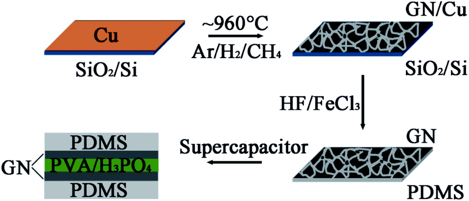 | ||
| Fig. 1 Schematic illustration of the procedures for the growth and transfer of the large scale graphene network (GN) along with the flexible and transparent all-solid-state supercapacitor constructed by sandwiching PVA–H3PO4 electrolyte between two PDMS-supported GN electrodes. | ||
2.2 Transfer process of graphene network
To transfer the GN from the silicon wafer, the as-synthesized sample on silicon wafer (GN/Cu/SiO2/Si, Fig. 1) was immersed into an aqueous solution of hydrofluoric acid at a concentration of 20 wt% (HF, Sigma-Aldrich, 48 wt% in H2O) for 30 min. As the SiO2 layer was etched by HF solution, the GN/Cu film gradually separated from the silicon wafer, floating on the surface of the HF solution as a free-standing film.To transfer the free-standing GN/Cu film onto PDMS and to remove the underlying Cu,29,30 we prepared the PDMS film by pouring the “base” and the “curing agent” at a ratio of 10![[thin space (1/6-em)]](https://www.rsc.org/images/entities/char_2009.gif) :1 (Sylgard 184, Dow Corning) into a plastic dish, which was followed by mixing and thermal curing at 75 °C for 1 hour. The free-standing GN/Cu film was then physically adhered by the solidified PDMS film from the top surface because graphene strong adheres to PDMS. Finally, pure GN on the PDMS substrate was obtained without obvious structural damage after etching Cu in the FeCl3 solution for 1 hour, followed by thorough washing with deionized (DI) water. A similar procedure was also used to transfer pure GNs onto silicon wafers for electron microscopic characterization.
:1 (Sylgard 184, Dow Corning) into a plastic dish, which was followed by mixing and thermal curing at 75 °C for 1 hour. The free-standing GN/Cu film was then physically adhered by the solidified PDMS film from the top surface because graphene strong adheres to PDMS. Finally, pure GN on the PDMS substrate was obtained without obvious structural damage after etching Cu in the FeCl3 solution for 1 hour, followed by thorough washing with deionized (DI) water. A similar procedure was also used to transfer pure GNs onto silicon wafers for electron microscopic characterization.
2.3 Fabrication of supercapacitors using graphene network electrodes
Prior to supercapacitor assembling, the PDMS-supported GN film was cut into small pieces (3 cm × 1.5 cm) to be used as both current collectors and electrodes. A gel solution containing polyvinyl alcohol (PVA) (1.0 g) and H3PO4 (1.0 g) in water (10.0 mL) was used as both electrolyte and separator. The gel electrolyte solution was directly drop-coated onto the GN film, followed by solvent evaporation under atmosphere for 6 hours. Thereafter, two pieces of the PDMS-supported GN films coated with the PVA–H3PO4 electrolyte were assembled under compression (Fig. 1). For the device testing without damaging GN, a copper wire was connected to a small portion of the GN electrode free from electrolyte using silver paste.2.4 Characterization
The GN samples were characterized by Raman spectroscopy with 514 nm laser (Renishaw). Scanning electron microscope (SEM, JEOL JSM-6510LV/LGS operated at 20 kV) was employed to characterize the GN morphology. The optical properties of graphene electrodes and supercapacitor were measured on spectrophotometer (Jasco V-670), and the electrochemical properties of supercapacitors were measured on CH Instruments 760C electrochemical workstation.3. Results and discussion
First, the Cu network was formed by annealing the 300 nm-thick sputter-coated copper film on silicon wafer at a controlled temperature during the first step of the two-step CVD (Fig. S1†). Scanning electron microscope (SEM) images given in Fig. S2† show that isolated dot-like and finger-like copper domains formed at 1000 °C and 970 °C, respectively, in accordance with the previous results reported by Ismach et al.31 As seen in Fig. 2, Cu network structure was not formed until the temperature was reduced to 960 °C. It was further observed that the macroscopic structure of the Cu network on the silicon wafer could be regulated to certain extent by adjusting the flow rate of Ar during the first step of the two-step CVD (Fig. 2 and S1†). The estimated area ratio of Cu coverage, and hence the GN coverage, was found to increase with increasing Ar flow rate (Fig. S3†). A similar increase in the surface coverage ratio could also be observed for the GN as graphene was deposited on the surface of the copper network.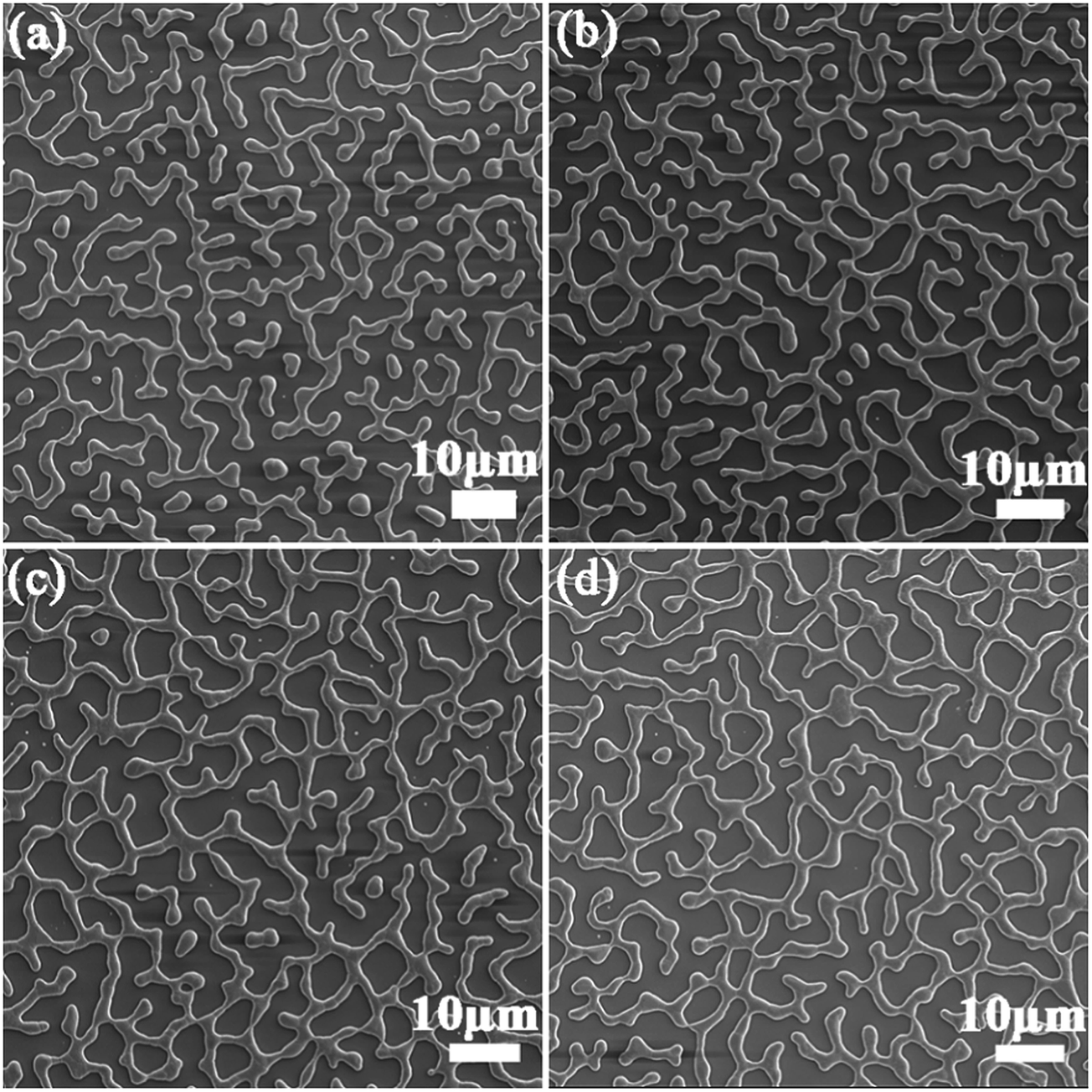 | ||
| Fig. 2 SEM images of the copper networks generated from 300 nm-thick copper coatings by heating at 960 °C for 180 s under Ar under different flow rates. From (a) to (d), Ar flow rates are 50, 100, 200, and 400 sccm, respectively. | ||
During the second step of the two-step CVD, a thin film of few-layer graphene grew on the Cu network formed in the first step. As shown in Fig. 3, the width of graphene ribbons within the GN formed on the copper substrate is about 1–2 μm. The average hole size within the GN ranges from 5 to 10 μm. The results show that the Cu network acted as the catalyst to support the graphene growth. Continued decomposition of CH4 led to the generation of active H radicals, which could also etch carbonaceous materials to exposure the catalyst surface covered by the grown graphene for initializing the new nucleation of graphene and increasing graphene layer numbers.32 Raman spectroscopic measurements at different locations on the as-synthesized GN (Fig. 3e and f) clearly show that graphene was deposited on the Cu network but not in the Cu-free regions. Raman spectra recorded on the Cu network (i.e., points 1, 2, and 3 in Fig. 3e) exhibit the D, G and 2D bands with a significantly higher G band intensity (IG) than that of the D band (ID) (Fig. 3f), indicating the presence of high-quality graphene on the Cu network. In Fig. 3f, the intensity ratios ID/IG and IG/I2D are 0.5 and 1.3 respectively, which prove to be several layers graphene. The layer number of graphene thus formed could be controlled by adjusting the deposition time during the step 2 of the two-step CVD. As can be seen from Raman spectra shown in Fig. S4,† the G to 2D peak intensity ratio increased from 0.8 to 2.4 with increasing CVD time, indicating that the layer number of graphene increased from 2–4 layers to 8–10 layers as the exposure time to carbon source increased from 30 s to 120 s. However, the intensity ratio of D band (ID) to G band (IG) remains 0.3–0.5, showing more defects existing in the graphene network than that of the planar graphene sheet, which are attributable to the numerous edge-defects in the network of graphene compared with the planar graphene sheet. Unlike many other complex patterning methods,33 this newly developed, simple, two-step CVD allows the direct formation of highly conductive GNs with a well-connected network structure, which are promising to be used as transparent and/or flexible electrode materials for various applications, as exemplified by flexible and transparent all-solid-state supercapacitors developed in the present study (vide infra).
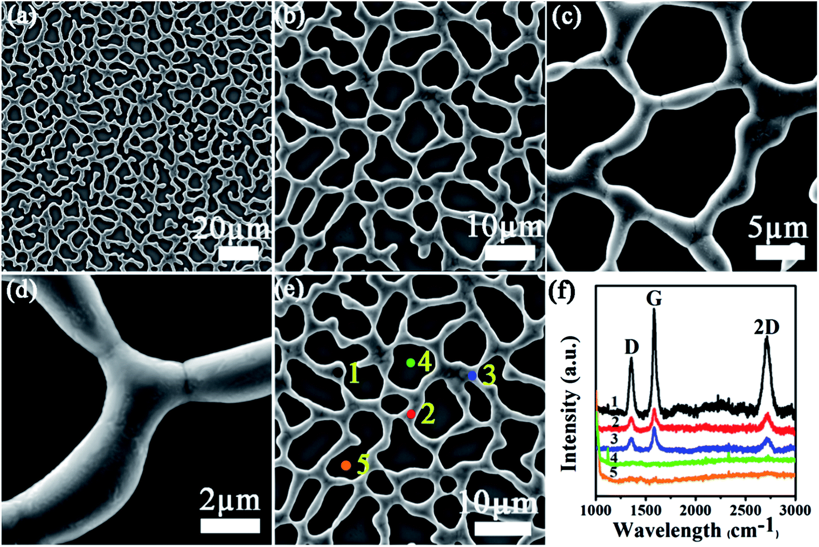 | ||
| Fig. 3 SEM images and Raman spectroscopy of GN deposited on the Cu network substrate. (a) and (b) SEM images of the GN on the Cu network substrate at low magnification; (c and d) SEM images of the GN on the Cu substrate at high magnification; (e) SEM image of a sample with 300 nm Cu after 120 s CVD growth, showing the morphology of the graphene on metal network; (f) Raman spectra measured at five different points marked with different coloured dots in (e). | ||
Prior to the fabrication of the GN-based supercapacitors, pure GNs after removing the underlying Cu layer were further subjected to electron microscopic characterization. The SEM images of the GN network transferred onto a clean silicon wafer given in Fig. S5† show wrinkles across graphene ribbons within the GN, presumably resulting from the surface-tension-induced shrinking/collapsing of the free-standing graphene surface during the transfer/Cu-etching processes. Instead of breaking network integrity, the shrinkage and wrinkle formation near the cross-section points could actually make the GN network even stronger.
Fig. 4a and b show the SEM images of the PDMS-supported GN network, from which it can be seen that the network of graphene maintained its interconnected structure, although with some distortion, after being transferred on the PDMS substrate. Raman spectra for the PDMS-supported GN given in Fig. 4c also show that no clear change occurred with respect to that of the as-synthesized GN on the Cu network (Fig. 3f) or pure GN transferred on silicon wafer (Fig. S4†), apart from some additional background signals from the PDMS substrate. Because of its unique network structure, the GN film transferred on the PDMS substrate is highly transparent. As seen in Fig. 4d, the 4-layer GN films on PDMS showed a high transmittance of ∼86% at 550 nm wavelength, while the transmittance of the 10-layer GN film was ∼75%. Both of them are significantly higher than that of a pin-hole free multi-layer graphene sheet on the similar PDMS substrate reported previously.10 In addition to the excellent optical transparency, the GN film also exhibited high flexibility. The changes in electrical resistance were measured while bending the PDMS-supported GN film to different angles. The electric resistance of the GN film is ranging from 4–6 kΩ cm−1, which is considerably higher than that of a single-sheet, multi-layer graphene sheet10 because of its porous structure. Fig. 4e and f show that the change in electrical resistance of the PDMS-supported GN was lower than 40% when it was bent to the highest possible deformation angles in both clockwise and anticlockwise directions, suggesting very good flexibility.
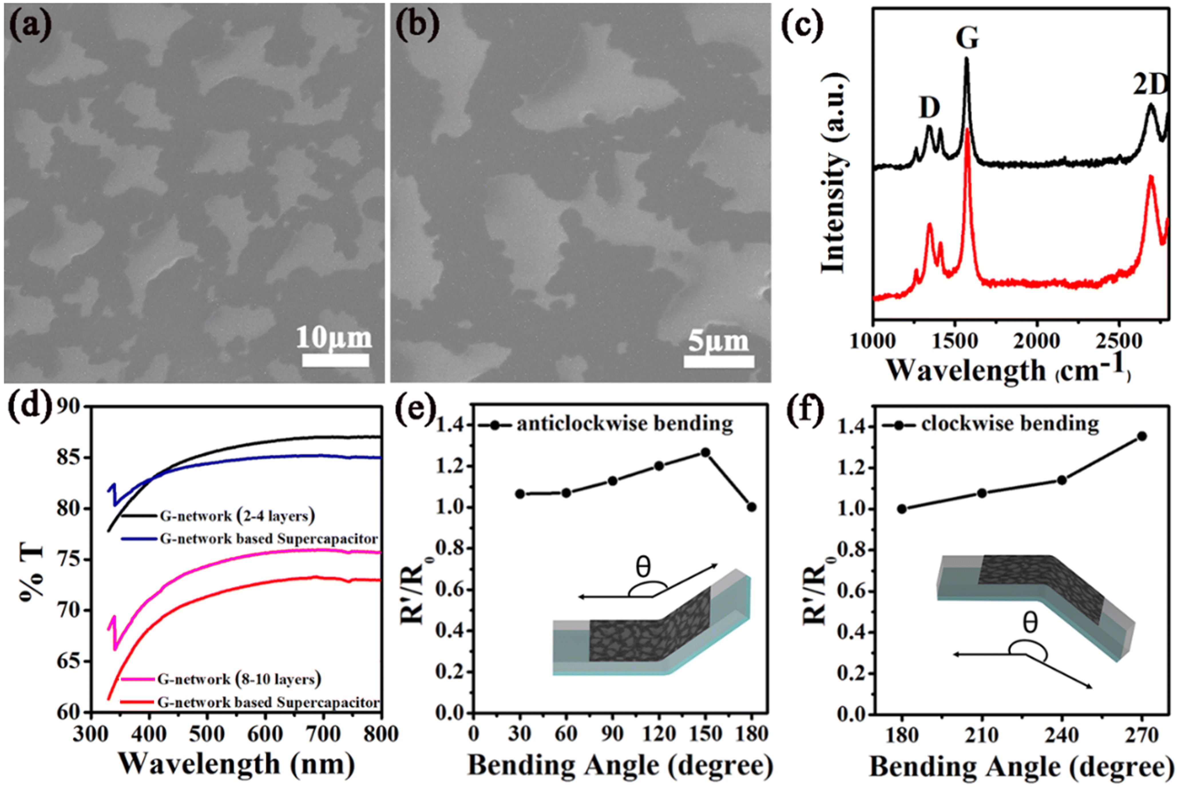 | ||
| Fig. 4 (a and b) SEM images of the GN films transferred on the PDMS substrate; (c) Raman spectra of the PDMS-supported GN films with two different layer numbers; (d) optical transmittance of the 2–4 layers and 8–10 layers layer GN films on the PDMS substrate. (e) and (f) Dependence of the two-electrode electrical resistance of GN films on the PDMS substrate at different bending angles in anticlockwise and clockwise directions, respectively. | ||
Using these highly transparent and flexible PDMS-supported GN films as electrodes, we developed flexible and transparent all-solid-state supercapacitors, in which a polymer gel (PVA–H3PO4, 1:1 wt/wt) was used as both the electrolyte and the separator. The all-solid-state supercapacitor was assembled by pressing two of the electrolyte-coated GN films supported by the PDMS substrate. Because of the high transparency of the PDMS-supported GN film (Fig. 4d and 5a) and the polymer electrolyte, the assembled supercapacitor (Fig. 5b) shows high transparency with a transmittance of ∼84% for electrodes with the 2–4 layers GN and ∼72% for that of 8–10 layers (Fig. 4d).
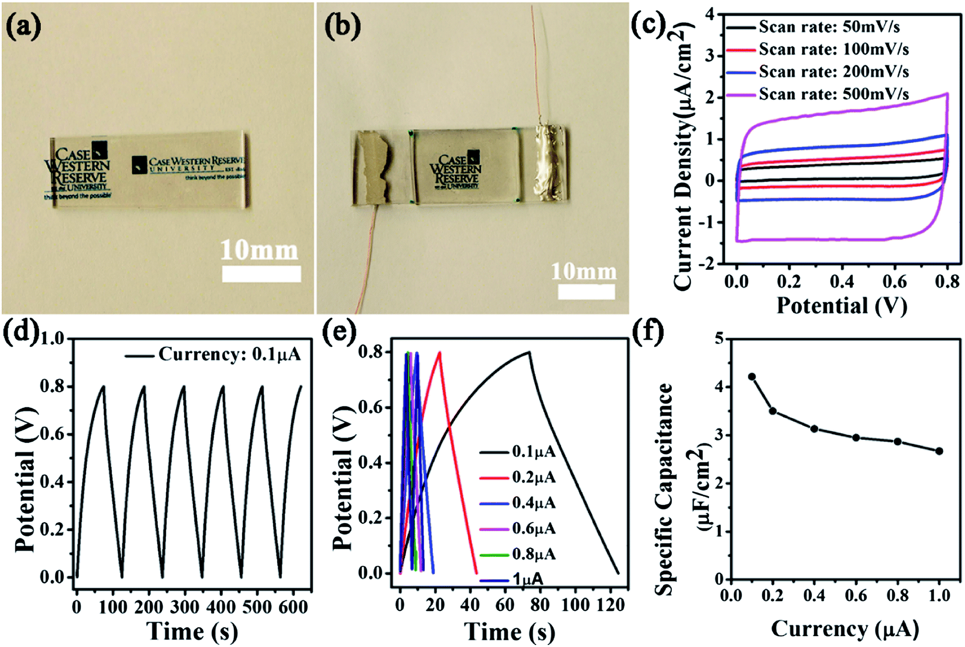 | ||
| Fig. 5 (a and b) Optical digital photograph of the GN films on PDMS and the transparent supercapacitor based on the GN films; (c) CV curves of a typical supercapacitor measured at the scan rate from 50 to 500 mV s−1; (d) galvanostatic charge–discharge (GCD) curve of the device measured at a constant current of 0.1 μA. (e) GCD curves of the device recorded at different applied currents; (f) variation of specific capacitance as a function of the applied current. | ||
Fig. 5c shows cyclic voltammetry (CV) curves of such a supercapacitor based on the GN film electrodes measured at scan rate ranging from 50 mV s−1 to 500 mV s−1, which indicates an excellent capacitive behaviour with a nearly rectangular shape even at a high scan rate of 500 mV s−1. Galvanostatic charge–discharge (GCD) curves given in Fig. 5d and e for flexible and transparent supercapacitor show triangular shapes, again suggesting nearly ideal capacitive behaviours. The area specific capacitance (Csp) was calculated using the equation Csp = IΔt/SΔV, where I is the applied current, Δt is the discharging time, S is the area of the active electrode in supercapacitor, and ΔV is the voltage window. From the GCD curves shown in Fig. 5d and e, the calculated surface-specific capacitances were 4.2 μF cm−2 at a discharge current of 0.1 μA and 2.7 μF cm−2 at 1.0 μA (Fig. 5f), which were close to those of the transparent devices based on uniform multi-layer graphene sheets but better optical transmittance because of the unique network structure.10 Comparing with uniform graphene films, the GN films possess an apparently reduced surface area for charge storage. However, the network structure could not only significantly facilitate the electrolyte transport but could also impart the edge-effect34 to effectively enhance supercapacitor performance. Therefore, the resultant supercapacitor based on the newly-developed GN films showed comparable performance with the multi-layer uniform graphene sheet.10
4. Conclusion
In summary, we have developed a simple two-step CVD approach to highly transparent and flexible two-dimensional graphene network films, which can be readily transferred onto various substrates (e.g., rigid silicon wafer and flexible polymer substrates) in large scale for a variety of applications, including wearable electronics and advanced energy storage. Because of its unique porous and interconnected network structure, such graphene network film transferred on the PDMS substrate showed a transmittance of up to 86% at 550 nm wavelength and excellent flexibility. Furthermore, flexible and transparent all-solid-state supercapacitors based on the graphene network electrodes showed a high transmittance of 84% and a high area specific capacitance of up to 4.2 μF cm−2. Because of its unique conductive network structure with high transparency and flexibility, the graphene network films developed in this study should also be very promising for several other applications, including, but not limited to, mechanical sensors, wearable electronics, and integrated energy conversion and storage devices.Acknowledgements
The authors are grateful for financial support from AFOSR (FA9550-12-1-0069; FA9550-12-1-0037) and NSF (CMMI-1266295; DMR-1106160).Notes and references
- P. Simon and Y. Gogotsi, Nat. Mater., 2008, 7, 845–854 CrossRef CAS PubMed.
- G. P. Wang, L. Zhang and J. J. Zhang, Chem. Soc. Rev., 2012, 41, 797–828 RSC.
- L. M. Dai, Acc. Chem. Res., 2013, 46, 31–42 CrossRef CAS PubMed.
- T. Chen and L. Dai, Mater. Today, 2013, 16, 272–280 CrossRef CAS PubMed.
- M. F. El-Kady, V. Strong, S. Dubin and R. B. Kaner, Science, 2012, 335, 1326–1330 CrossRef CAS PubMed.
- Y. M. He, W. J. Chen, C. T. Gao, J. Y. Zhou, X. D. Li and E. Q. Xie, Nanoscale, 2013, 5, 8799–8820 RSC.
- Y. Chen, X. Zhang, H. T. Zhang, X. Z. Sun, D. C. Zhang and Y. W. Ma, RSC Adv., 2012, 2, 7747–7753 RSC.
- P. Si, S. J. Ding, X. W. Lou and D. H. Kim, RSC Adv., 2011, 1, 1271–1278 RSC.
- T. Chen, H. S. Peng, M. Durstock and L. Dai, Sci. Rep, 2014, 4, 3612 Search PubMed.
- T. Chen, Y. H. Xue, A. K. Roy and L. Dai, ACS Nano, 2014, 8, 1039–1046 CrossRef CAS PubMed.
- I. Nam, S. Park, G. P. Kim, J. Park and J. Yi, Chem. Sci., 2013, 4, 1663–1667 RSC.
- A. K. Geim, Science, 2009, 324, 1530–1534 CrossRef CAS PubMed.
- A. K. Geim and K. S. Novoselov, Nat. Mater., 2007, 6, 183–191 CrossRef CAS PubMed.
- K. S. Novoselov, V. I. Fal'ko, L. Colombo, P. R. Gellert, M. G. Schwab and K. Kim, Nature, 2012, 490, 192–200 CrossRef CAS PubMed.
- K. S. Novoselov, A. K. Geim, S. V. Morozov, D. Jiang, Y. Zhang, S. V. Dubonos, I. V. Grigorieva and A. A. Firsov, Science, 2004, 306, 666–669 CrossRef CAS PubMed.
- K. S. Kim, Y. Zhao, H. Jang, S. Y. Lee, J. M. Kim, K. S. Kim, J. H. Ahn, P. Kim, J. Y. Choi and B. H. Hong, Nature, 2009, 457, 706–710 CrossRef CAS PubMed.
- X. Li, W. Cai, J. An, S. Kim, J. Nah, D. Yang, R. Piner, A. Velamakanni, I. Jung, E. Tutuc, S. K. Banerjee, L. Colombo and R. S. Ruoff, Science, 2009, 324, 1312–1314 CrossRef CAS PubMed.
- A. Reina, X. Jia, J. Ho, D. Nezich, H. Son, V. Bulovic, M. S. Dresselhaus and J. Kong, Nano Lett., 2008, 9, 30–35 CrossRef PubMed.
- S. Y. Bae, I. Y. Jeon, J. Yang, N. Park, H. S. Shin, S. Park, R. S. Ruoff, L. Dai and J. B. Baek, ACS Nano, 2011, 5, 4974–4980 CrossRef CAS PubMed.
- J. Kim, L. J. Cote and J. X. Huang, Acc. Chem. Res., 2012, 45, 1356–1364 CrossRef CAS PubMed.
- I. Y. Jeon, Y. R. Shin, G. J. Sohn, H. J. Choi, S. Y. Bae, J. Mahmood, S. M. Jung, J. M. Seo, M. J. Kim, D. W. Chang, L. Dai and J. B. Baek, Proc. Natl. Acad. Sci., 2012, 109, 5588–5593 CrossRef CAS PubMed.
- I. Y. Jeon, H. J. Choi, S. M. Jung, J. M. Seo, M. J. Kim, L. Dai and J. B. Baek, J. Am. Chem. Soc., 2013, 135, 1386–1393 CrossRef CAS PubMed.
- J. L. Liu, C. K. Poh, D. Zhan, L. F. Lai, S. H. Lim, L. Wang, X. X. Liu, N. G. Sahoo, C. M. Li, Z. X. Shen and J. Y. Lin, Nano Energy, 2013, 2, 377–386 CrossRef CAS PubMed.
- J. L. Liu, H. P. Yang, S. G. Zhen, C. K. Poh, A. Chaurasia, J. S. Luo, X. Y. Wu, E. K. L. Yeow, N. G. Sahoo, J. Y. Lin and Z. X. Shen, RSC Adv., 2013, 3, 11745–11750 RSC.
- Z. P. Chen, W. C. Ren, L. B. Gao, B. L. Liu, S. F. Pei and H. M. Cheng, Nat. Mater., 2011, 10, 424–428 CrossRef CAS PubMed.
- Y. H. Xue, J. Liu, H. Chen, R. G. Wang, D. Q. Li, J. Qu and L. Dai, Angew. Chem., Int. Ed., 2012, 51, 12124–12127 CrossRef CAS PubMed.
- J.-S. Lee, H.-J. Ahn, J.-C. Yoon and J.-H. Jang, Phys. Chem. Chem. Phys., 2012, 14, 7938–7943 RSC.
- N. Li, Z. P. Chen, W. C. Ren, F. Li and H. M. Cheng, Proc. Natl. Acad. Sci., 2012, 109, 17360–17365 CrossRef CAS PubMed.
- S. Bae, H. Kim, Y. Lee, X. F. Xu, J. S. Park, Y. Zheng, J. Balakrishnan, T. Lei, H. R. Kim, Y. I. Song, Y. J. Kim, K. S. Kim, B. Ozyilmaz, J. H. Ahn, B. H. Hong and S. Iijima, Nat. Nanotechnol., 2010, 5, 574–578 CrossRef CAS PubMed.
- Y. Lee, S. Bae, H. Jang, S. Jang, S. E. Zhu, S. H. Sim, Y. I. Song, B. H. Hong and J. H. Ahn, Nano Lett., 2010, 10, 490–493 CrossRef CAS PubMed.
- A. Ismach, C. Druzgalski, S. Penwell, A. Schwartzberg, M. Zheng, A. Javey, J. Bokor and Y. Zhang, Nano Lett., 2010, 10, 1542–1548 CrossRef CAS PubMed.
- D. Geng, B. Wu, Y. Guo, L. Huang, Y. Xue, J. Chen, G. Yu, L. Jiang, W. Hu and Y. Liu, Proc. Natl. Acad. Sci., 2012, 109, 7992–7996 CrossRef CAS PubMed , and references cited therein.
- Y. Zhou and K. P. Loh, Adv. Mater., 2010, 22, 3615–3620 CrossRef CAS PubMed.
- W. J. Yuan, Y. Zhou, Y. R. Li, C. Li, H. L. Peng, J. Zhang, Z. F. Liu, L. Dai and G. Q. Shi, Sci. Rep., 2013, 3, 2248 Search PubMed.
Footnote |
| † Electronic supplementary information (ESI) available: SEM images, TEM images and Raman spectra of graphene network. See DOI: 10.1039/c4ra05076b |
| This journal is © The Royal Society of Chemistry 2014 |