DOI:
10.1039/D3TC00626C
(Paper)
J. Mater. Chem. C, 2023,
11, 6597-6606
Magnetically driven hierarchically ordered carbonyl iron@SiO2/Ni@Ag/silicone rubber composite film for enhanced electromagnetic interference shielding with ultralow reflection†
Received
19th February 2023
, Accepted 24th April 2023
First published on 10th May 2023
Abstract
Flexible electromagnetic interference (EMI) shielding materials are highly desired for wearable electronic devices and military equipment. Meanwhile, to reduce the secondary electromagnetic pollution caused by the reflected electromagnetic waves (EMWs), these materials are required to possess strong EMW absorption capacities. However, it still remains a big challenge for flexible shielding materials to achieve absorption-dominated EMI shielding and maintain effective performances under large tensile strain. Herein, we propose a novel strategy for ultralow-reflection EMI shielding composite films made by magnetically driven hierarchically ordered alignment of carbonyl iron@SiO2 (CS) and Ni@Ag (NA) in silicone rubber. Flaky carbonyl iron was coated with SiO2 to prepare CS microparticles, and magnetic alignment was applied within silicon rubber to obtain a highly ordered absorption layer. Then, NA microparticles were magnetically aligned to integrate with the CS layer to construct the CSNA composite film. In this case, the EMI shielding performances of the CSNA film under various strains (0–100%) were investigated in detail. Based on the unique absorption–reflection–reabsorption mechanism, an EMI shielding effectiveness (SE) of 64.5 dB with an ultralow reflected power coefficient (R = 0.044) could be achieved in the unstretched state and reached ∼38.6 dB even at 100% strain. This work provides a new strategy to fabricate highly efficient adsorption-dominated flexible EMI shielding materials, indicating great potential for EMI shielding applications under large strain.
1. Introduction
Due to the rapid development of wearable electronics, wireless communication, and military equipment, there is an increasingly urgent demand for flexible EMI shielding materials that can guarantee the functions of electronic devices and also reduce EMW damage.1–5 Currently, most flexible EMI shielding materials are constructed with thermoplastic polyurethanes (TPU),6 polydimethylsiloxane (PDMS),7 polyvinyl alcohol (PVA),8 natural rubber (NR),9 polymer nanofibers,10–12 and silicone rubber (SR).13 Among them, silicone rubber is especially preferred to construct EMI shielding materials and also electromagnetic (EM) metamaterials due to its good flexibility and stretchability, low cost, and excellent chemical stability, such as corrosion/aging resistance.14,15 Despite the advances in silicone rubber-based EMI shielding materials (SRMs), their initial reflection-dominated mechanism will inevitably lead to secondary EMW pollution, in which shielding and effective absorption are simultaneously desired.16 Constructing multi-layer EMI shielding materials has been proven to be an effective method to overcome these blocks.17–19 Inspired by this, SRMs prepared with various conductive fillers and absorbents (e.g., CNT, graphene, and Fe3O4) have achieved effective EMW absorption, yet sufficient EMI SE is fairly difficult to achieve due to their low intrinsic conductivity.20–22 Therefore, it is demanding to develop novel SRMs to achieve absorption-dominated EMI shielding and maintain effective performances under large tensile strain.
Previous research studies have verified that ordered alignment of the fillers can improve the electrical conductivity and electromagnetic properties of the composites via magnetic, electric, or flow field induced alignment.23–25 Magnetic field-induced alignment is suitable for large-density alignment of micro-/nanoparticles in a viscous matrix due to its features of cost-efficiency, non-contact safeness, and high penetration.26 Despite the development of constructing aligned EMI shielding composites in low-viscosity matrixes (e.g., TPU, PDMS, epoxy resin), magnetic alignment-based highly ordered SRMs have not been reported to the best of our knowledge.27–29 In this work, magnetic alignment of EM microparticles was utilized to construct multi-layer, highly flexible, adsorption-dominated SRMs. In general, good magnetism is a prerequisite for microparticles to serve as EMW absorbers, such as ferrites (e.g., CoFe2O4, Fe3O4),30,31 carbonyl iron (CI),32 and metals (e.g., Fe, Co, Ni).33,34 Among them, CI microparticles stand out due to their excellent magnetization properties and easy large-scale preparation. To broaden the effective absorption band of CI microparticles, SiO2 nanoparticles could be coated on their surfaces to endow them strong dielectric loss and good chemical stability.35 Besides, magnetic microparticles (e.g., Fe, Co, Ni) with superior electrical conductivity are ideal candidates to serve as EMI shielding fillers. Herein, Ni@Ag (NA) microparticles with enhanced electrical conductivity are utilized to construct the second layer of SRMs with a lower addition ratio.36
In this study, we propose multilayered absorption-dominant EMI shielding composite films via magnetically driven hierarchically ordered alignment of CS and NA microparticles in SR. A series of CS microparticles were synthesized with different precursor ratios, and magnetic alignment was performed to obtain a highly ordered absorption layer. After that, NA microparticles were magnetically aligned to construct the integrated CSNA composite film. The mechanical properties, electrical conductivity, and EMI shielding performance of the as-prepared films were measured under diverse tensile strains. Significantly, the EMW reflection was greatly reduced owing to the highly ordered CS absorption layer and the unique absorption–reflection–reabsorption mechanism. Due to the high performance and facile fabrication, the CSNA composite film demonstrated potential for EMI shielding applications including wearable electronic devices and morphing aircraft sealing.
2. Experimental procedures
2.1. Materials
CI microparticles (average size = 5 μm) were supplied by Shenyang Hangda Technology Co., Ltd (Shenyang, China). NA microparticles (average size = 15 μm) were purchased from Guangzhou Yinfeng Metal Technology Co., Ltd (Guangzhou, China). 3-Aminopropyltriethoxysilane (APTES), tetraethyl orthosilicate (TEOS), and ethanol (C2H6O) were obtained from Lan Yi Chemical Reagent Co., Ltd (Beijing, China). Silicone rubber (E625) was provided by Hongyejie Technology Co., Ltd (Shenzhen, China).
2.2. Preparation of CS microparticles
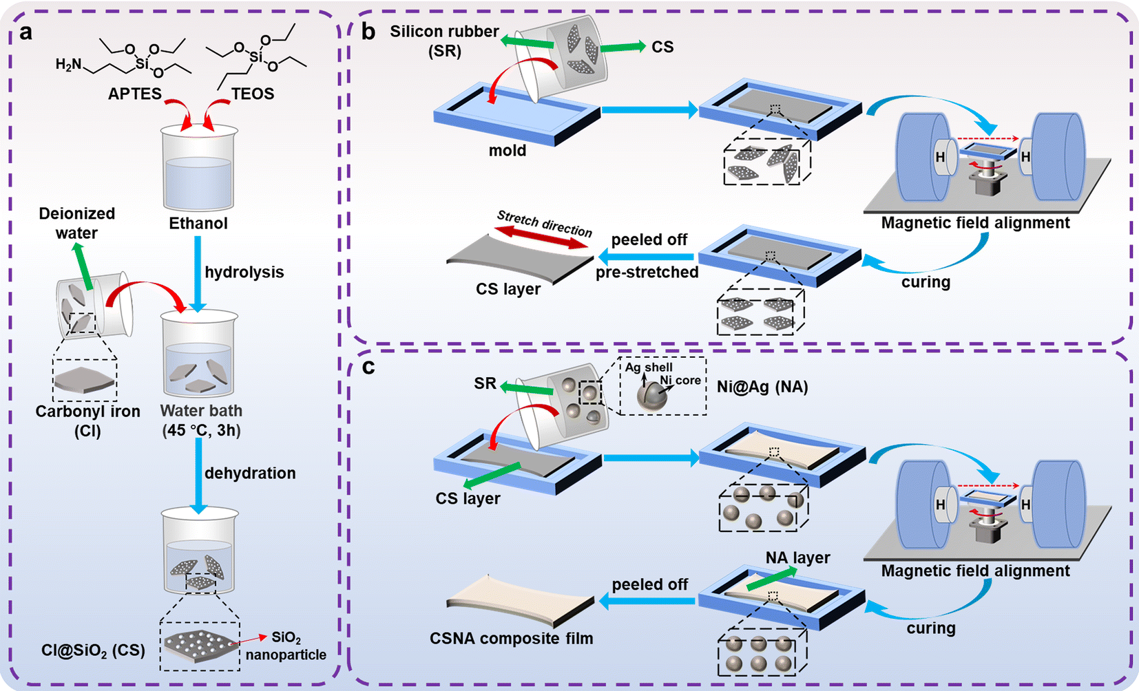
APTES (6 mL) and TEOS, according to their volume ratios of 1![[thin space (1/6-em)]](https://www.rsc.org/images/entities/char_2009.gif) :X (X = 2, 3, or 5), were added to ethanol (2500 mL) and well mixed to prepare a homogeneous solution. CI microparticles (10 g) were added into deionized water (300 mL) to form a suspension after ultrasonic stirring for 1 h. Then, the CI suspension was uniformly mixed with the APTES/TEOS ethanol solution, and kept in a water bath (45 °C, 3 h, mechanical stirring) for chemical reaction. In this process, APTES and TEOS were hydrolyzed to produce silanol molecules, which were further dehydrated with hydroxyl groups on the surface of CI to form Si–O bonds. Finally, SiO2 layers were deposited onto CI microparticles, and a series of CS microparticles were obtained after the centrifuging, washing, and drying treatments. The as-prepared CS microparticles were named CS-2, CS-3, and CS-5, respectively, which correspond to the volume ratio value of APTES to TEOS.
:X (X = 2, 3, or 5), were added to ethanol (2500 mL) and well mixed to prepare a homogeneous solution. CI microparticles (10 g) were added into deionized water (300 mL) to form a suspension after ultrasonic stirring for 1 h. Then, the CI suspension was uniformly mixed with the APTES/TEOS ethanol solution, and kept in a water bath (45 °C, 3 h, mechanical stirring) for chemical reaction. In this process, APTES and TEOS were hydrolyzed to produce silanol molecules, which were further dehydrated with hydroxyl groups on the surface of CI to form Si–O bonds. Finally, SiO2 layers were deposited onto CI microparticles, and a series of CS microparticles were obtained after the centrifuging, washing, and drying treatments. The as-prepared CS microparticles were named CS-2, CS-3, and CS-5, respectively, which correspond to the volume ratio value of APTES to TEOS.
2.3. Preparation of CS layers
CS-3 (5.0 g) microparticles were mixed with 5.0 g SR. After thoroughly stirring, the elastomer was poured into the mold and placed on the rotating platform (speed = 2.5 Hz). A static magnetic field (intensity = 250 mT) powered by a pair of electromagnets was employed to align the mixture for 1.5 h, and the CS layer was obtained after the SR was cured and peeled off from the mold.
2.4. Preparation of CSNA composite films
The as-fabricated CS layer was pre-stretched at 100% strain along the length direction and then fixed within the mold. Then, NA microparticles (6.5 g) were mixed with 3.5 g SR and poured on top of the CS layer. After that, they were placed on the rotating platform (speed = 0.75 Hz) in a magnetic field (intensity = 250 mT) for 2 hours. Finally, the CSNA composite film (80 mm × 25 mm × 1.6 mm) could be obtained when the SR was completely cured. In this case, the single-layered CS and NA layers were also fabricated using the same fabrication technique and magnetic treatment as mentioned above. Besides, the unaligned CSNA composite film was also prepared without magnetic alignment. A schematic diagram of the preparation process is shown in Fig. 1.
 |
| | Fig. 1 Schematics of the preparation process of the CSNA composite film. | |
2.5. Characterization
Scanning electron microscopy (SEM; Hitachi S-4800) and transmission electron microscopy (TEM; Tecnai G2 F20 S-TWIN) were applied to analyze the morphology and structure of the specimens. Energy dispersive spectroscopy (EDS; HORIBA EX-350) was used to determine the elemental composition. X-ray diffraction (XRD; Bruker D8) with Cu-Kα radiation was used to determine the composition and crystallinity. Raman spectra were collected using a Renishaw in-via spectrometer excited with a 532 nm laser. X-ray photoelectron spectroscopy (XPS; Thermo Scientific Escalab 250Xi) was employed to investigate the chemical bonds of the samples. Fourier transform infrared spectroscopy (FTIR; Nicolet IS10) was applied to explore the functional group and chemical structure of the samples. A vibrating scanning magnetometer (VSM; MPMS3) was used to analyze the magnetic properties of the CS and NA microparticles. A 3D microscopy system (Keyence, VHX-6000) was employed to evaluate the 3D surface morphology of the stretched NA layer.
Besides, the CS microparticles mixed thoroughly with SR were poured into toroidal cylinders molds (Φin = 3.04 mm and Φout = 7.0 mm) and aligned with the magnetic field (2.5 Hz, 250 mT, 1.5 h). A vector network analyzer (Ceyear, AV3672B) was used to assess the EM properties of the CS samples in the frequency range of 2–18 GHz via the coaxial line method. In addition, the EM parameters of the unaligned CS samples were also measured. A universal testing device (Instron 5966) with a constant speed of 50 mm min−1 was used to examine the mechanical properties of the CSNA film at room temperature. The tensile strength was measured with an initial length of 65 mm according to a typical standard method.37 The electrical conductivities of the CSNA composite film were investigated using multi-point probe resistivity testing equipment (HELPASS, HPS-2662). The EMI SE of the CSNA sample under different strains was analyzed in the X-band using the waveguide method by the vector network analyzer. A dynamic tensile device, including a slide block with clamping device, guide rail, and ball screw driven by a stepper motor, was attached to the vector network analyzer to carry out the EMI shielding test. Furthermore, the EMI SE of the NA layer, CS layer, and unaligned CSNA composite film were also measured for comparison.
3. Results and discussion
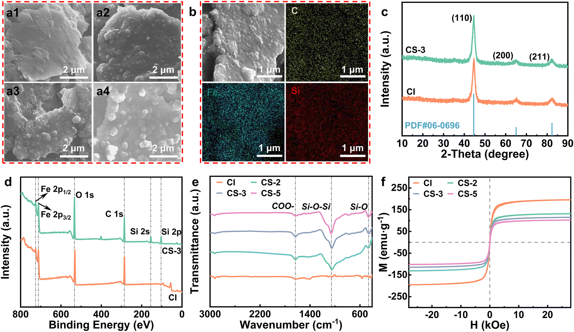
The SEM images of the CI and CS microparticles are shown in Fig. 2a. Compared with CI, it could be seen that a layer of SiO2 was coated on the surface of CS. In this case, SiO2 nanoparticles on the surfaces of CS microparticles exhibited larger sizes from CS-2 to CS-5, since more TEOS molecules were adsorbed and hydrolyzed for SiO2 nucleation.38 EDS images of the CS-3 sample revealed a uniform distribution of the Si element, indicating that a SiO2 layer was successfully coated on the CI surface (Fig. 2b). The elemental contents of CI and CS samples are also shown in Fig. S1 (ESI†). With the deposition of SiO2 nanoparticles on the CI surfaces, Fe element decreased yet the Si element increased. Besides, a TEM image of the CS-3 microparticles is shown in Fig. S2 (ESI†), and the SiO2 nanoparticles could be seen on the surface of the CI particles. The XRD results of the CI and CS-3 samples are displayed in Fig. 2c, and three diffraction peaks at 44.7°, 65.0°, and 82.32° were identified as the (110), (200), and (211) crystal planes of α-Fe, respectively (JCPDS No. 06-0696).39 There were no obvious characteristic peaks for SiO2 nanoparticles due to their amorphous state. The XPS results revealed that both CI and CS-3 samples exhibited four characteristic peaks, which were assigned to C 1s (284.7 eV), O 1s (531.6 eV), Fe 2p3/2 (710.2 eV), and Fe 2p1/2 (724.3 eV), respectively (Fig. 2d).35 This was ascribed to the chemical composition of CI microparticles. In addition, Si 2p (102.2 eV) and Si 2s (153.2 eV) could be observed in the CS-3 sample, which further confirmed the existence of the SiO2 nanoparticles.40 To investigate the chemical bonds of CS-3 microparticles, high-resolution XPS spectra were obtained, as shown in Fig. S4 (ESI†). The C 1s spectrum could be deconvoluted into two characteristic peaks, identified as C–C (284.7 eV) and C–O (288.6 eV).41 The O 1s spectrum was also divided as Fe2O3 (529.7 eV), C–O (531.4 eV), and Si–O (532.4 eV).42 Besides, the chemical bond percentage of the CS-3 sample was also calculated and shown in Table S1 (ESI†). Moreover, FTIR spectroscopy was used to determine the functional groups of the CS and CI microparticles, which are shown in Fig. 2e. The peaks of all samples appeared at 1644 cm−1 could be attributed to the asymmetric stretching vibration of the COO– bond of CI microparticles.43 For CS microparticles, the peaks appeared at 446 cm−1 and 1046 cm−1 corresponding to Si–O and Si–O–Si of SiO2 nanoparticles, respectively.44 Furthermore, as shown in Fig. 2f, the hysteresis loops showed that the saturation magnetization of CS decreased gradually with the increase in the Si element of the samples displayed in Fig. S1 (ESI†). Both CI and CS microparticles possessed high saturation magnetization with minor coercivity, which facilitated the desired alignment under the magnetic field.
 |
| | Fig. 2 SEM images of (a1) CI, (a2) CS-2, (a3) CS-3, and (a4) CS-5. (b) EDS images of CS-3, (c) XRD and (d) XPS results of CI and CS-3, (e) FTIR and (f) VSM results of all the microparticles. | |
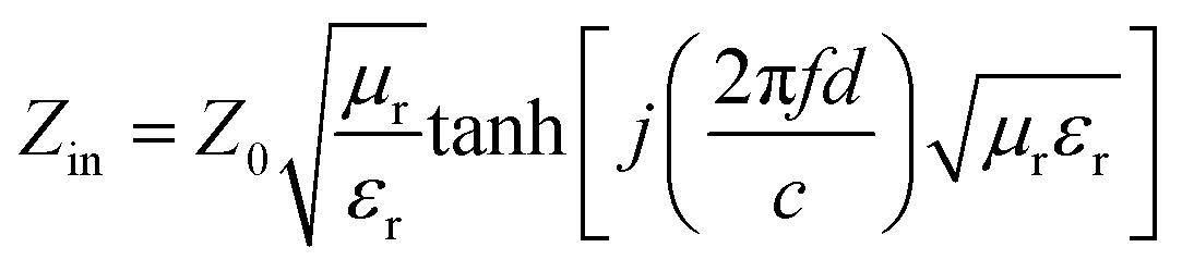
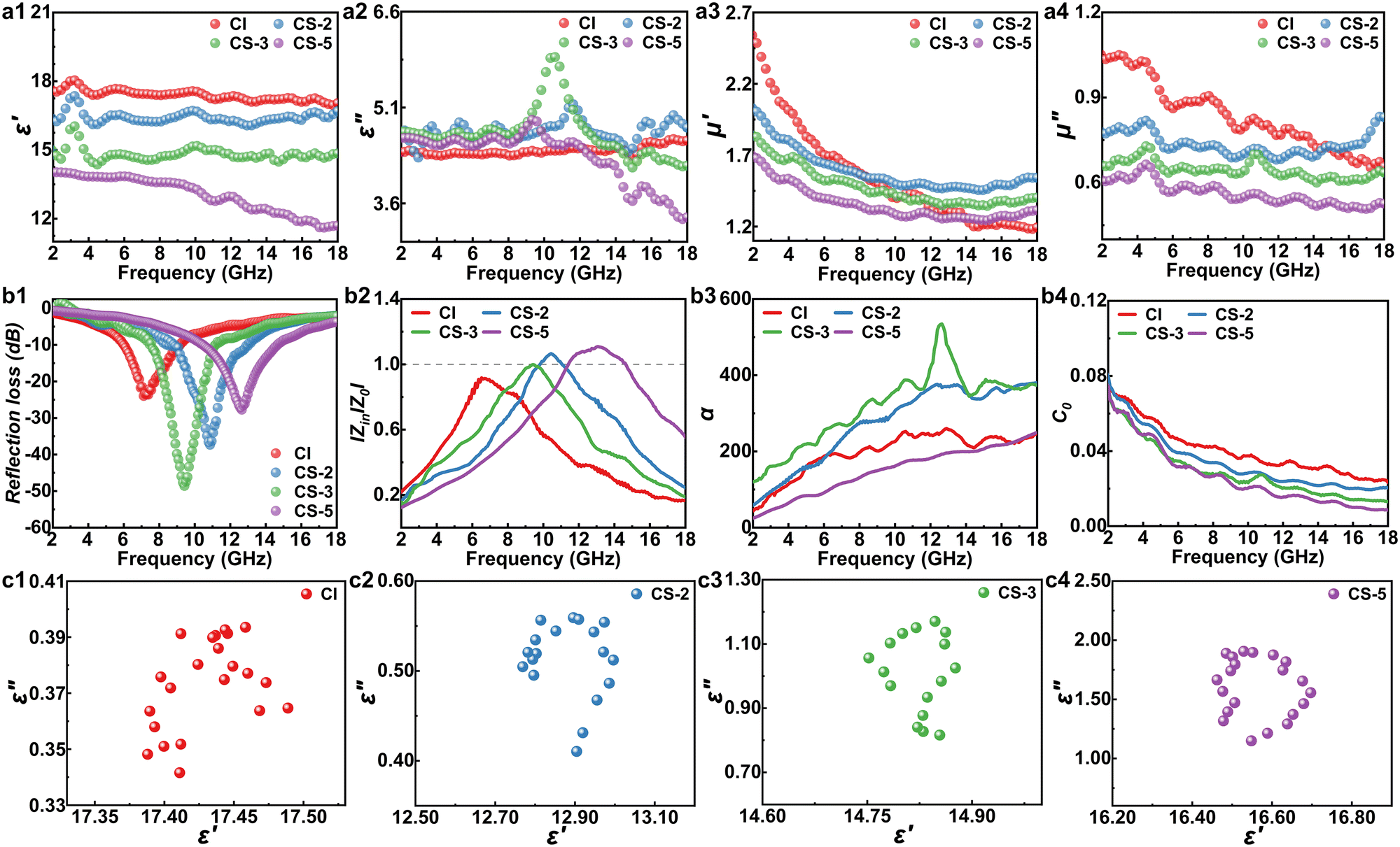
To explore the EM properties of the CS samples after the magnetic field-induced alignment process, their EM parameters were measured in detail. The real part (ε′, μ′) of complex permittivity and permeability represents the storage capacity of EM energy, and the imaginary part (ε′′, μ′′) of them stands for the capability to dissipate EM energy.45 After being aligned, the ε′ and ε′′ values of the CS samples displayed in Fig. 3a1–a2 were significantly higher than those of the unaligned ones (Fig. S6b, ESI†). This was due to the fact that the alignment would increase the electronic polarization of the CS microparticles.28 Therefore, the complex permittivity and dielectric loss of the CS samples were significantly enhanced. In particular, the CS-3 sample had a larger ε′′ among the CS samples, which should be attributed to the strong interface polarization introduced by the SiO2 layers.39 All the CS samples showed obvious dielectric loss peaks in Fig. 3a2 in the 8–12 GHz range, suggesting the enhanced dielectric loss properties of the CS microparticles, which should be attributed to the strong interface polarization and improved interface impedance matching. Furthermore, the CS-3 sample exhibited a larger loss peak, which corresponded to its excellent dielectric loss capability. Appropriate SiO2 nanoparticle loading could give the CS particles strong interfacial polarization loss without affecting the conductivity of the CI matrix. The complex permeabilities (μ′, μ′′) of all the samples are shown in Fig. 3a3–a4, and the values of the aligned CS samples were higher than those of the unaligned ones (Fig. S6c, ESI†). This could be attributed to the parallel alignment of the easy-magnetization planes of the flake-shaped EM microparticles, leading to an increase in their permeability.46 Based on the measured EM parameters of the samples, the following equations were used to determine their reflection loss (RL) values:45
| |  | (1) |
| |  | (2) |
where the inherent impedance of open space and the input are marked as
Z0 and
Zin, respectively. In addition,
f indicates the frequency,
c denotes the light speed, and
d represents the thickness. The EMW absorption properties of samples are displayed in
Fig. 3b1. Among them, CS-3 exhibited the best EMW absorption performance with a RL
min value of −48.57 dB at 9.42 GHz (thickness = 1.0 mm, mass ratio = 50 wt%). A broad effective absorption band of about 3.55 GHz (7.63–11.18 GHz) was also achieved. Therefore, CS-3 microparticles were used to carry out follow-up research. Furthermore, the RL values of CS samples were significantly lower than those of unaligned CS samples (Fig. S6d, ESI
†), which was attributed to the orderly alignment of CS microparticles that greatly contributed to the dielectric and magnetic loss.
The |Zin/Z0| values of all the samples are shown in Fig. 3b2. When the |Zin/Z0| value is close to 1, almost no EMW reflects at air-absorbent interfaces, and most can be attenuated by the absorbers. In this case, the |Zin/Z0| value of CS-3 was about 1 at 9.42 GHz, indicating that it had the best impedance matching condition among all samples. To evaluate the EMW attenuation capability of the prepared absorbers, their attenuation constants (α) were calculated as:47
| |  | (3) |
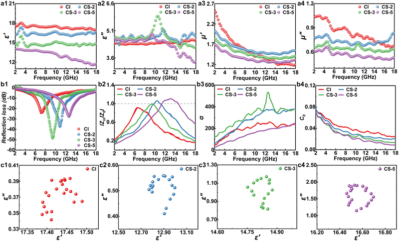 |
| | Fig. 3 (a1–a4) EM parameters (ε′, ε′′, μ′, μ′′), (b1) RL value, (b2) impedance ratio (|Zin/Z0|), (b3) attenuation coefficient (α), (b4) C0 curve, and (c1–c4) Cole–Cole semicircle of the CI and CS samples (thickness = 1 mm, mass ratio = 50 wt%). | |
As shown in Fig. 3b3, CS-3 showed a larger α value than other samples in the 2–18 GHz band, confirming the enhanced dielectric and magnetic loss capabilities introduced by the SiO2 nanoparticles. To evaluate the magnetic loss mechanism of the samples, their eddy current loss (C0) values were estimated using the below formula:47
If the C0 value remains consistent at 2–18 GHz, this suggests that the magnetic loss capability of the absorbers is solely attributable to eddy current loss. However, it was obvious that the C0 values of all the samples gradually decreased in the 2–10 GHz band (Fig. 3b4), indicating that eddy current loss and magnetic resonance were both responsible for the magnetic loss of all the samples.31 Besides, dielectric loss also affected their EMW absorption performance. The Cole–Cole plots exhibited in Fig. 3c1–c4 were used to analyze the dielectric relaxation processes. Each Cole–Cole semicircle indicated a Debye relaxation process. It could be seen that all CS samples had an obvious semicircle feature, whereas the CI sample did not. This implied that the SiO2 nanoparticles gave CI strong interface polarization relaxation, which could enhance the dielectric loss of the CS microparticles.
The cross-sectional SEM images of the CSNA composite film is shown in Fig. 4a. The two layers of ordered materials corresponded to CS (∼1.0 mm thickness) and NA (∼0.6 mm thickness) layers, respectively. The partially enlarged images revealed that the flaky CS microparticles and spheroid NA microparticles were layered and orderly distributed in the SR matrix after magnetic field-induced alignment (Fig. 4b1–b2). The characterization results of NA microparticles are also shown in Fig. S3 (ESI†). NA microparticles had an average size of 15 μm and were composed of Ni (65.41 wt%) and Ag (34.59 wt%) elements. As a comparison, the SEM images of unaligned CS and NA layers are displayed in Fig. S6a and S7a (ESI†), respectively. Besides, EDS images displayed the cross-sectional elemental (Fe, Ag, and Ni) distribution of the CSNA composite film (Fig. 4c). The photos of the CSNA film showed that it possessed an excellent deformation ability, and could be easily coiled and twisted (Fig. 4d). The tensile stress–strain test demonstrated that CSNA had good stretchability, and its breaking strength and elongation percentage were 4.88 MPa and 202.7%, respectively (Fig. 4e). Furthermore, electrical conductivities at various strain conditions of the CSNA composite film are shown in Fig. 4f. Its high conductivity (385.6 S cm−1) under the 0% strain state was attributed to the dense conductive networks induced by the pre-stretching process. However, its conductivity decreased significantly as the tensile strain increased but could still be kept at 36.8 S cm−1 under 100% strain. In this case, a small LED could be lit up by the CSNA connected DC circuit, and could still keep illuminated even under 50% strain, which further verified the superior electrical conductivity of the CSNA composite film.
 |
| | Fig. 4 (a) Cross-sectional SEM images of the CSNA film and enlarged view of the selected area of (b1) CS layer and (b2) NA layer, (c) EDS images, (d) original, coiled and twisted states, (e) stress–strain curve, and (f) electrical conductivity at different strain conditions of the CSNA film (the inset illustration shows the digital photos of the CSNA circuit to light up the LED). | |
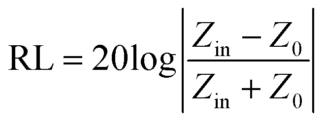
The EMI shielding performances of the CSNA composite film under different strain conditions are displayed in Fig. 5. The R (reflection), A (absorption), and T (transmission) power coefficients could be calculated based on the S parameters (S11, S21) measured by the vector network analyzer according to the formula: R = (S11)2, T = (S21)2, A = 1−T−R. Besides, SET (total), SER (reflection), SEA (absorption), and SEM (multi-reflection, neglected when SET > 15 dB) could be obtained using the following equations:48
| | | SER = −10lg(1 − R) | (5) |
| |  | (6) |
As demonstrated in
Fig. 5a, the SE
T value of the CSNA film at strain-0% condition was maintained around 63 dB in the X band (8.2–12.4 GHz), and the largest value of 64.5 dB could be achieved at 9.34 GHz, suggesting that 99.999999% of the EMW could be shielded. With the tensile strain increasing, the SE
T value of the CSNA was decreasing gradually. However, even when the tensile strain reached 100%, its SE
T value was kept at approximately 38.6 dB, which was enough to meet the commercial standard.
48 The testing records of the CSNA samples under various strains (0%, 50%, and 100%) using the typical waveguide method were also shown in the inner illustrations. It was obvious that the CSNA had a higher SE
T value than the unaligned CSNA sample (Fig. S7b, ESI
†), suggesting that the EMI shielding performance could be greatly enhanced
via the magnetic field-induced alignment. Besides, the hierarchically ordered absorption and shielding structure provided the CSNA with a better EMI shielding performance than that of the single-layered NA and CS samples. SE
A and SE
R values of the CSNA film are shown in
Fig. 5b. The SE
R value under 0% strain was kept at a low level (<1.18 dB), owing to the high efficiency of EMW absorption by the CS layer. However, as the tensile strain increased, the SE
R value steadily increased and the SE
A value gradually decreased, indicating that the EMW absorption performance of the CSNA was weakened. The average EMI SE showed that the SE
T value was in the range of 32.27–63.35 dB in the range of 0–100% strain (
Fig. 5c). The
R and
A values of the CSNA composite film were used to evaluate its EMI shielding mechanism (
Fig. 5d and e). The lowest
R value under 0% strain was only 0.044 at 9.34 GHz, showing that only 4.4% of EMWs were reflected and most of them were absorbed. The average power coefficients are depicted in
Fig. 5f, and the
T value remained low under the strain range of 0–100%, implying that the CSNA film had an excellent EMI shielding performance. Furthermore, the average
R value increased when the strains increased, which could be attributed to the density decrease of CS microparticles (Fig. S8, ESI
†). The
A/
R value was used to measure the EMI shielding mechanism of the CSNA under various strains. It can be seen from
Fig. 5g that the CSNA at the strain-0% condition had a high
A/
R value of 5.10, suggesting a strong absorption-dominated shielding mechanism.
49 In the strain range of 25–50%, CSNA showed an absorption-dominated shielding mechanism. However, the EMI shielding mechanism transformed into reflection-dominated characteristics in the 50–100% strain range. The comparison of the EMI shielding performances of the CSNA composite film and other flexible shielding materials reported in the references is displayed in
Fig. 5h.
20–22,50–63 The CSNA film prepared in this work exhibited a higher SE and a lower
R value than them, indicating outstanding EMI shielding and a significant reduction in EMW secondary pollution.
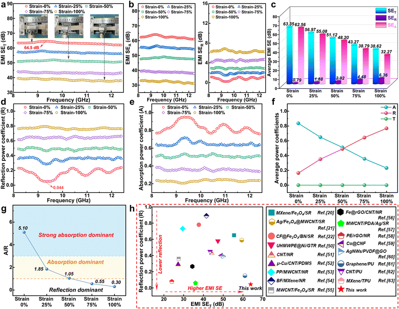 |
| | Fig. 5 (a) SET, (b) SER and SEA, and (c) average EMI SE. Power coefficient of (d) reflection (R), (e) absorption (A), and (f) average values, (g) A/R of the CSNA composite film under different strain conditions (0–100%). (h) Comparison of the EMI SE and the R value of CSNA in this work with other flexible EMI shielding materials. | |
To investigate the effects of the morphologies and the microparticle density of the NA layer on the EMI shielding performance of the CSNA film under different tensile strains, its SEM images and 3D morphologies were analyzed. From the SEM images (Fig. 6a, c, and e), it was clear that as the tensile strain increased, the NA microparticles separated and the density decreased, resulting in a less dense conductive network. Then, electron transmission changed from relying on close adjacent contacts to electron hopping.64 As a result, the conductivity and SET value decreased (Fig. 3f and 4a). The 3D surface morphologies revealed that the NA layer at the strain-0% state had many convex wrinkles, and the maximum height was about 100.79 μm (Fig. 6b). Wrinkles were formed by shrinkage of the NA layer poured on the pre-stretched CS layer when the CSNA was released to the free state, which stored a certain amount of pre-deformation for the CSNA film in the Z-direction. When the tensile strain increased to 100%, the wrinkles were stretched and flattened, and their maximum height was reduced to 51.98 μm (Fig. 6f). Meanwhile, the pre-deformation accumulated by the wrinkles in the Z direction was released and unfolded along the X–Y direction, which was favorable for maintaining the high density of the NA conductive microparticles in the X–Y plane. Therefore, the CSNA composite film could preserve effective EMI shielding performance under large strains.
 |
| | Fig. 6 SEM images and 3D morphologies of the NA layer in the CSNA composite film at different strains of (a and b) 0%, (c and d) 50%, and (e and f) 100%. | |
To demonstrate the EMI shielding performance of the CSNA film, custom wireless electromagnetic transmission devices were used, as shown in Fig. 7a and b. The Tesla coil supplied by DC power could emit high-frequency EMW, and the induced high voltage could ionize the neon gas in the lamp to stimulate glow discharge.65Fig. 7a shows that when the Tesla coil was energized, the neon lamps on the left and right sides were lit up. As shown in Fig. 7b, the CSNA composite film was used to shield the EMW transmitted to the right neon lamp, then the lamp was turned off while the one on the left remained light. This phenomenon indicated that the CSNA film had a highly efficient EMI shielding performance. Schematics of the EMI shielding mechanism of the CSNA composite film are shown in Fig. 7c. The incident EMWs were absorbed while penetrating the CS layer on the upper part of the CSNA film. The excellent absorption performance should be attributed to the synergistic effect of the strong magnetic loss (magnetic resonance and eddy current loss) and the dielectric loss (interface polarization) of the CS microparticles. Then, the transmitted EMWs entered the NA layer, where a portion of them was attenuated by the electron conduction loss (including hopping and migrating). Furthermore, the reflected EMWs went into the CS layer via multiple reflections and scattering, which were then absorbed again. In general, this absorption–refection–reabsorption mechanism endowed the CSNA composite film a high-efficiency EMI SE of 64.5 dB and an ultralow R value of 0.044, suggesting that most of the EMWs were absorbed instead of being reflected to the surrounding environment.
 |
| | Fig. 7 A digital photograph of the wireless power-transfer device (a) without and (b) with CSNA composite film, and (c) schematics of the EMI shielding mechanism of the CSNA composite film. | |
4. Conclusions
In this work, a multilayered absorption-dominant EMI shielding composite film was fabricated via magnetically driven, hierarchically ordered alignment of CS and NA microparticles in SR. We synthesized a series of CS microparticles with different precursor ratios and conducted magnetic alignment to obtain a highly ordered absorption layer. The results indicated that the CS-3 sample had the best absorption capability, with a RLmin value of −48.57 dB at 9.42 GHz. After that, NA microparticles were further magnetically aligned to construct the integrated CSNA composite film. The film exhibited excellent stretchability with a high breaking strength (4.88 MPa) and elongation percentage (202.7%). The wrinkles in the pre-stretched NA layer could store a certain pre-deformation capacity, which was conducive to maintaining effective EMI shielding under large strain. The well-aligned film exhibited absorption-dominated shielding in the strain range of 0–50%, indicating that the secondary EMW radiation could be effectively reduced. It could achieve a highly effective EMI SE (64.5 dB) with an ultralow reflected power coefficient (R = 0.044) in the unstretched state and maintain EMI shielding of 38.6 dB even at 100% strain. Generally, our research might provide an effective and facile strategy to prepare flexible EMI shielding composite films with high efficiency and ultralow reflection, which are promising for practical applications in various fields.
Author contributions
Teng Chen: conceptualization, investigation, visualization, validation, and writing – original draft. Jun Cai: funding acquisition, writing – review & editing, and supervision. De Gong: methodology, writing – review & editing, and supervision. Xiang Cheng: validation. Peng Liu: data curation. Deyuan Zhang: supervision.
Conflicts of interest
There are no conflicts to declare.
Acknowledgements
This work was supported by the National Natural Science Foundation of China (Grant No. 52205298, 51775022), the Project funded by China Postdoctoral Science Foundation (Grant No. 2022M710302, 2022TQ0023), the BEIGE Institute (BGI2022-05), and the Fundamental Research Funds for the Central Universities.
References
- Y. Xie, S. Liu, K. Huang, B. Chen, P. Shi, Z. Chen, B. Liu, K. Liu, Z. Wu, K. Chen, Y. Qi and Z. Liu, Adv. Mater., 2022, 34, 2202982 CrossRef CAS PubMed
 .
.
- M. Cheng, M. Ying, R. Zhao, L. Ji, H. Li, X. Liu, J. Zhang, Y. Li, X. Dong and X. Zhang, ACS Nano, 2022, 16, 16996–17007 CrossRef CAS PubMed .
- K. Zhang, L. Zheng, M. A. Aouraghe and F. Xu, Adv. Compos. Hybrid Mater., 2022, 5, 872–883 CrossRef CAS .
- R. Dilli, M. L. R. Chandra and D. Jordhana, Eng. Sci., 2021, 16, 308–318 Search PubMed .
- G. Qi, Y. Liu, L. Chen, P. Xie, D. Pan, Z. Shi, B. Quan, Y. Zhong, C. Liu, R. Fan and Z. Guo, Adv. Compos. Hybrid Mater., 2021, 4, 1226–1238 CrossRef CAS .
- W. Zhai, C. Wang, S. Wang, J. Li, Y. Zhao, P. Zhan, K. Dai, G. Zheng, C. Liu and C. Shen, J. Mater. Chem. A, 2021, 9, 7238–7247 RSC .
- A. De and B. B. Khatua, J. Mater. Chem. C, 2022, 10, 3863–3875 RSC .
- Y. Zhang, K. Ruan and J. Gu, Small, 2021, 17, 2101951 CrossRef CAS PubMed .
- M. Fan, S. Li, L. Wu, L. Li, M. Qu, J. Nie, R. Zhang, P. Tang and Y. Bin, Chem. Eng. J., 2022, 433, 133499 CrossRef CAS .
- M. Miao, R. Liu, S. Thaiboonrod, L. Shi, S. Cao, J. Zhang, J. Fang and X. Feng, J. Mater. Chem. C, 2020, 8, 3120–3126 RSC .
- Y. Han, K. Ruan and J. Gu, Angew. Chem., Int. Ed., 2023, 62, e202216093 CAS .
- J. Zhou, S. Thaiboonrod, J. Fang, S. Cao, M. Miao and X. Feng, Nano Res., 2022, 15, 8536–8545 CrossRef CAS .
- D. Liu, Q.-Q. Kong, H. Jia, L.-J. Xie, J. Chen, Z. Tao, Z. Wang, D. Jiang and C.-M. Chen, Carbon, 2021, 183, 216–224 CrossRef CAS .
- J. Yang, X. Liao, G. Wang, J. Chen, P. Song, W. Tang, F. Guo, F. Liu and G. Li, Compos. Sci. Technol., 2021, 206, 108663 CrossRef CAS .
- H. Wu, H. Sun, F. Han, P. Xie, Y. Zhong, B. Quan, Y. Zhao, C. Liu, R. Fan and Z. Guo, Eng. Sci., 2022, 17, 113–120 CAS .
- H. Wu, C. Zhu, X. Li, X. Hu, H. Xie, X. Lu and J.-P. Qu, Macromol. Rapid Commun., 2022, 43, 2200387 CrossRef CAS PubMed .
- M. Ma, X. Liao, Q. Chu, S. Chen, Y. Shi, H. He and X. Wang, Compos. Sci. Technol., 2022, 226, 109540 CrossRef CAS .
- H. Liu, Z. Wang, Y. Yang, S. Wu, C. Wang, C. You and N. Tian, J. Mater. Sci. Technol., 2022, 130, 75–85 CrossRef .
- N. Duan, Z. Shi, J. Wang, X. Zhang, C. Zhang, C. Zhang and G. Wang, Appl. Surf. Sci., 2023, 613, 156038 CrossRef CAS .
- H. Li, X. Ru, Y. Song, H. Wang, C. Yang, S. Zheng, L. Gong, X. Zhang, H. Duan, Z. Liu, Q. Zhang and Y. Chen, Ind. Eng. Chem. Res., 2022, 61, 11766–11776 CrossRef CAS .
- J. Yang, X. Liao, G. Wang, J. Chen, F. Guo, W. Tang, W. Wang, Z. Yan and G. Li, Chem. Eng. J., 2020, 390, 124589 CrossRef CAS .
- Y. Guo, H. Qiu, K. Ruan, S. Wang, Y. Zhang and J. Gu, Compos. Sci. Technol., 2022, 219, 109253 CrossRef CAS .
- D. Gong, L. Sun, X. Li, W. Zhang, D. Zhang and J. Cai, Small Struct., 2023, 2200356, DOI:10.1002/sstr.202200356 .
- C. Lee, S. M. Park, S. Kim, Y.-S. Choi, G. Park, Y. C. Kang, C. M. Koo, S. J. Kim and D. K. Yoon, Nat. Commun., 2022, 13, 5615 CrossRef CAS PubMed .
- A. Gebrekrstos, S. Biswas, A. V. Menon, G. Madras, P. Pötschke and S. Bose, Composites, Part B, 2019, 166, 749–757 CrossRef CAS .
- D. Gong, N. Celi, D. Zhang and J. Cai, ACS Appl. Mater. Interfaces, 2022, 14, 6320–6330 CrossRef CAS PubMed .
- S. Y. Hong, Y. C. Kim, M. Wang, J.-D. Nam and J. Suhr, Eur. Polym. J., 2020, 127, 109595 CrossRef CAS .
- C. Liu, J. Cai, Y. Duan, X. Li and D. Zhang, J. Magn. Magn. Mater., 2018, 458, 116–122 CrossRef CAS .
- X. Li, H. Zhao, C. Liu, J. Cai, Y. Zhang, Y. Jiang and D. Zhang, Adv. Opt. Mater., 2019, 7, 1900247 CrossRef .
- J. He, S. Liu, L. Deng, D. Shan, C. Cao, H. Luo and S. Yan, Appl. Surf. Sci., 2020, 504, 144210 CrossRef CAS .
- T. Chen, J. Cai, D. Gong, C. Liu, P. Liu, X. Cheng and D. Zhang, J. Alloys Compd., 2023, 935, 168085 CrossRef CAS .
- Q.-Q. Hu, L. Chai, K. Liang, Y.-X. Jiang, G. Yang, L.-B. Zhang, L.-J. Yin, X. Wang, T. Liu, H.-P. Lu and L.-J. Deng, Rare Met., 2023, 42, 558–571 CrossRef CAS .
- J. Xu, Y. Shi, X. Zhang, H. Yuan, B. Li, C. Zhu, X. Zhang and Y. Chen, J. Mater. Chem. C, 2020, 8, 7847–7857 RSC .
- J. Xu, Y. Zhao, Y. Chen, Y. Chen, Z.-H. Xie and P. R. Munroe, ACS Appl. Mater. Interfaces, 2022, 14, 42468–42482 CrossRef CAS PubMed .
- N. Zhang, Y. Wang, P. Chen and W. Chen, J. Colloid Interface Sci., 2021, 581, 84–95 CrossRef CAS PubMed .
- X. Liu, Z. Ye, L. Zhang, P. Feng, J. Shao, M. Zhong, Z. Chen, L. Ci, P. He, H. Ji, J. Wei, M. Li and W. Zhao, J. Mater. Sci., 2021, 56, 5570–5580 CrossRef CAS .
- X. Yan, G. R. Hamed and L. Jia, Polymer, 2017, 125, 172–181 CrossRef CAS .
- K. S. Sista, S. Dwarapudi, D. Kumar, G. R. Sinha and A. P. Moon, J. Alloys Compd., 2021, 853, 157251 CrossRef CAS .
- H. Wang, M. Wang, X. Zhang, Z. Lu, W. Fu, B. Zhong, C. Wang, J. Zou, X. Huang and G. Wen, Surf. Interfaces, 2020, 21, 100755 CrossRef CAS .
- Y. Zhou, H. Xie, W. Zhou and Z. Ren, J. Magn. Magn. Mater., 2018, 446, 143–149 CrossRef CAS .
- W. Huang, J. Wu, W. Guo, R. Li and L. Cui, J. Alloys Compd., 2007, 443, 48–52 CrossRef CAS .
- L. Lefèvre, T. Belmonte, T. Czerwiec, A. Ricard and H. Michel, Appl. Surf. Sci., 2000, 153, 85–95 CrossRef .
- K. Sun, S. Feng, Q. Jiang, X. Li, Y. Li, R. Fan, Y. An and J. Wang, J. Magn. Magn. Mater., 2020, 493, 165705 CrossRef CAS .
- Y.-Y. Huang and J. Wu, Materials, 2022, 15, 484 CrossRef CAS PubMed .
- C. Ding, H. Fu, T. Wu, Y. Li, S. Wu, X. Ren, Z. Gao, K. Guo, L. Xia, G. Wen and X. Huang, J. Mater. Chem. A, 2022, 10, 17603–17613 RSC .
- S.-M. Na, J.-J. Park, S. Lee, S.-Y. Jeong and A. B. Flatau, Mater. Lett., 2018, 213, 326–330 CrossRef CAS .
- S. Dong, W. Tang, P. Hu, X. Zhao, X. Zhang, J. Han and P. Hu, ACS Sustainable Chem. Eng., 2019, 7, 11795–11805 CrossRef CAS .
- L. Chen, K. Guo, S.-L. Zeng, L. Xu, C.-Y. Xing, S. Zhang and B.-J. Li, Carbon, 2020, 162, 445–454 CrossRef CAS .
- Z. Zong, P. Ren, Z. Guo, J. Wang, Z. Chen, Y. Jin and F. Ren, J. Colloid Interface Sci., 2022, 619, 96–105 CrossRef CAS PubMed .
- A. Sheng, Y. Yang, W. Ren, H. Duan, B. Liu, G. Zhao and Y. Liu, J. Mater. Sci.: Mater. Electron., 2019, 30, 14669–14678 CrossRef CAS .
- Z. Xie, Y. Cai, Y. Zhan, Y. Meng, Y. Li, Q. Xie and H. Xia, Chem. Eng. J., 2022, 435, 135118 CrossRef CAS .
- Y. Wang, Q.-M. He, Y.-N. Gao, T.-N. Yue and M. Wang, Composites, Part A, 2022, 162, 107135 CrossRef CAS .
- T. Sharika, J. Abraham, M. Arif P, S. C. George, N. Kalarikkal and S. Thomas, Composites, Part B, 2019, 173, 106798 CrossRef .
- J. Yu, Z. Cui, J. Lu, J. Zhao, Y. Zhang, G. Fan, S. Liu, Y. He, Y. Yu and D. Qi, Composites, Part B, 2021, 224, 109193 CrossRef CAS .
- J. Yang, X. Liao, J. Li, G. He, Y. Zhang, W. Tang, G. Wang and G. Li, Compos. Sci. Technol., 2019, 181, 107670 CrossRef CAS .
- X.-Y. Li, P.-P. Zhao, L.-X. Han and C. Deng, Compos. Sci. Technol., 2022, 219, 109221 CrossRef CAS .
- Y. Song, A. Dattatray Phule, Z. Yu, X. Zhang, A. Du, H. Wang and Z. Xiu Zhang, Eur. Polym. J., 2021, 161, 110839 CrossRef CAS .
- Y. Sun, L. Ma, Y. Song, A. D. Phule, L. Li and Z. X. Zhang, Eur. Polym. J., 2021, 147, 110288 CrossRef CAS .
- D. Gao, S. Guo, Y. Zhou, B. Lyu, X. Li, P. Zhao and J. Ma, ACS Appl. Mater. Interfaces, 2022, 14, 38077–38089 CrossRef CAS PubMed .
- L. Jia, X. Ding, J. Sun, X. Zhang and X. Tian, Composites, Part A, 2022, 156, 106884 CrossRef CAS .
- Y. Li, J. Liu, S. Wang, L. Zhang and B. Shen, Composites, Part B, 2020, 182, 107615 CrossRef CAS .
- G. Wang, D. Yi, X. Jia, J. Chen, B. Shen and W. Zheng, Mater. Today Phys., 2022, 22, 100612 CrossRef CAS .
- Q. Gao, Y. Pan, G. Zheng, C. Liu, C. Shen and X. Liu, Adv. Compos. Hybrid Mater., 2021, 4, 274–285 CrossRef CAS .
- Y. Wang, R. Liu, J. Zhang, M. Miao and X. Feng, Appl. Surf. Sci., 2021, 546, 149143 CrossRef CAS .
- H. Guo, M. Zheng, X. Ma, R. Cao, K. Liu, W. Yang, S. Jian, S. Jiang and G. Duan, Compos. Commun., 2022, 31, 101130 CrossRef .
|
| This journal is © The Royal Society of Chemistry 2023 |
Click here to see how this site uses Cookies. View our privacy policy here. 
 ,
Jun
Cai
,
Jun
Cai