
Efficient and stable perovskite solar cells based on functional graphene-modified P3HT hole-transporting layer†
Jian Ye*a,
Xueliang Lib,
Jianjun Zhaoa,
Xuelan Meia and
Qian Lia
aDepartment of Chemistry and Environmental Engineering, Bengbu College, Bengbu, Anhui 233030, China. E-mail: bbyejian@126.com
bDepartment of Application Chemistry, School of Chemical Engineering, Hefei University of Technology, Hefei, Anhui 230009, China
First published on 6th April 2016
Abstract
Organic–inorganic perovskite solar cells have recently emerged at the forefront of photovoltaics research. With the focus mainly on efficiency, the aspect of mobility and stability has so far not been thoroughly addressed. In this paper, we identify mobility as a fundamental weak point of perovskite solar cells, and demonstrate a facile approach to enhance the hole mobility and conductivity by introducing the highly dispersed graphene in P3HT as the hole transporting layer. With this composite structure, we achieve power conversion efficiencies of up to 13.82%. Moreover, we observe excellent stability based on the P3HT/graphene layer due to its good hydrophobicity.
1. Introduction
Driven by the demand of developing third generation low-cost and high-efficiency solar cells, organic hybrid thin film solar cells have been widely studied.1–8 In recent years, a great breakthrough was made by replacing traditional organic materials with organic halide perovskite as active layer materials.2,9,10 A typical triiodide perovskite (CH3NH3PbI3)-based solar cells (PSCs) with an organic spiro-OMeTAD as the hole-transporting material (HTM) has been demonstrated to be very promising, with efficiencies of more than 20%.2,11 In spite of the high efficiency, there are some issues existing for the PSCs. One major drawback is spiro-OMeTAD is expensive; typically, it needs p-type doping for optimal cell performance.12–14 And CH3NH3PbI3 is its poor stability when exposed to moisture in air, which can be easily decomposed and lose its function even with an encapsulation.15–19Therefore, seeking suitable replacements of spiro-OMeTAD with advantages of low cost, ease of fabrication, and high performance of efficiency and stability, are urgent for the future application. Since the generation of the first perovskite solar cell, the exploration for cost effective HTMs has been continuously performed. P3HT is one of the most widely used donors in organic photovoltaic devices.20–22 In comparison with spiro-OMeTAD, P3HT is-dopant free and can be prepared without an extra oxidation process when applied in perovskite solar cells. As a result of its facile processing method and desirable hole conductivity, P3HT has been regarded as a good option for HTMs.23,24 However, it is well known that the HTM of PSCs is around of 100 nm thickness, and the conductivity of pure P3HT semiconductor is limited the hole transportation of PSCs. So to enhance the hole mobility and conductivity is important for P3HT HTMs to match with spiro-OMeTAD performance.
Herein, a highly dispersed functional graphene (F-graphene) has been employed to modify the P3HT hole transporting material of perovskite solar cell. The high mobility and conductivity of F-graphene can make a great contribution to HTMs for PSCs performance. Also, the relative interaction can enhance the hole mobility of P3HT polymer chains and modify the energy level of the device.25,26 As shown in Fig. 1, these P3HT/F-graphene composite HTM-based PSCs shows superior cell performance to the corresponding device with the pure P3HT under the same condition, a high PCE up to 13.82% has been achieved, with an 8 mm2 effective area. Moreover, the stability of the final device with P3HT/F-graphene composite HTM exhibits great stability under air atmosphere due to its hydrophobicity of the P3HT/F-graphene composite materials.
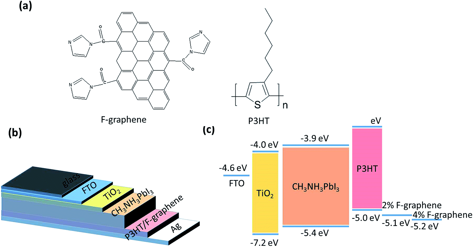 | ||
| Fig. 1 (a) The chemical structure of F-graphene, chemical structure of P3HT. (b) Schematic diagram of the perovskite solar cells with P3HT hole-transporting material modified with F-graphene. (c) The schematic energy diagram of the hole-transporting layer involved in the PSCs. | ||
2. Experimental section
Synthesis of functional graphene (F-graphene)
Function of graphene oxide by imidazole: 1 g GO was loaded in a 250 mL round bottom flask and water (100 mL) was then added, yielding an inhomogeneous yellow-brown dispersion. This dispersion was sonicated using an ultrasonic bath cleaner (150 W) until it became clear with no visible particulate matter. 5 g imidazole was added in the bottom flask. The solution heated in an oil bath at 118 °C under a water-cooled condenser for 24 h. This product was isolated by filtration over a medium fritted glass funnel, washed copiously with water (5 × 100 mL) and methanol (5 × 100 mL) to wash the residual imidazole, and dried in a vacuum refrigerant dryer for 24 hours to obtain functioned-graphene oxide (F-GO) powder. Reduction of functioned-graphene oxide by hydrazine hydrate: the reduction of F-GO by hydrazine hydrate is likely the function of GO. In a typical procedure, F-GO (100 mg) was loaded in a 250 mL round bottom flask and water (100 mL) was then added, yielding an inhomogeneous yellow-brown dispersion. This dispersion was sonicated using an ultrasonic bath cleaner (150 W) until it became clear with no visible particulate matter. Hydrazine hydrate (1.00 mL, 32.1 mmol) was then added and the solution heated in an oil bath at 100 °C under a water-cooled condenser for 24 h over which the reduced F-GO gradually precipitated out as a black solid. This product was isolated by filtration over a medium fritted glass funnel, washed copiously with water (5 × 100 mL) and methanol (5 × 100 mL), and dried in a vacuum refrigerant dryer for 24 hours to obtain reduced F-GO powder. Details of the synthesis procedure and characterization are shown in the ESI.†Device fabrication
The perovskite precursor solution was prepared by dissolved methylamine iodide (MAI, Sigma-Aldrich, 99%) and lead(II) iodide (PbI2, Sigma-Aldrich, 99%) in N,N-dimethylformamide (DMF, Sigma-Aldrich, HPLC) with final concentrations of 37 wt%. The perovskite solar cells were fabricated on F-doped indium oxide (FTO) pattern glass substrates (<15 Ω) with a traditional device configuration: FTO/TiO2/CH3NH3PbI3/P3HT/Ag. First, the FTO glass substrates were cleaned by sequential ultrasonic treatment in acetone, detergent, deionized water, and isopropyl alcohol for 10 min each and then dried with a nitrogen stream. Then the pre-clean FTO glass substrates were treated by ozone plasma treatment for 20 min. A 30 nm thick TiO2 blocking layer was sequentially spin coated twice from a solution containing 0.3 M in n-butyl alcohol. The mesoporous TiO2 layer was spin coated from a solution containing 1 g 18NRT dyesol paste in 7 mL of EtOH at 5000 rpm for 30 s. And the TiO2 coated substrates were annealing at 500 °C for 60 min. PbI2 solution (462 mg mL−1 in DMF) was spin-coated on TiO2 at a rate of 5000 rpm for 30 s in the N2 glovebox. PbI2 film was dipped in a solution of CH3NH3I in 2-propanol (10 mg mL−1) for 1 min to form CH3NH3PbI3 perovskite. Prepared perovskite were annealing at 100 °C for 15 min. The P3HT composite hole transporting layers were deposited on the perovskite layers by spin-coating at 3000 rpm with P3HT tetrahydrofuran solutions. Finally, 80 nm of Ag was thermally evaporated on top of the P3HT layer as counter electrode. The effective area of PSCs is 8 mm2.Characterization
For measuring the performance of the PSCs, simulated AM 1.5 sunlight was generated with a class AAA ABET solar simulator calibrated to give simulated AM 1.5 of 100 mW cm−2 equivalent irradiance, using an NREL-calibrated KG5 filtered silicon reference cell. X-ray diffraction (XRD) data was obtained from a Bruker Advanced X-ray diffractometer (40 kV and 30 mA) with CuKα radiation. UV/Vis absorption spectra of the resulting films were measured by a spectrophotometer (V-650, Jasco) with an integrating sphere. Morphologies of films were examined by FEI, XL30 S-FEG scanning electron microscope (SEM) at an accelerating voltage of 5 kV. Raman spectra were recorded on LabRAM HR Raman microscope with a laser excitation wavelength of 514.5 nm. XPS studies were performed on a ThermoVG Scientific ESCALAB 250 photoelectron spectrometer using a monochromated Al Kα (1486.6 eV) X-ray source. All recorded peaks were corrected for electrostatic effects by setting the C–C component of the C 1s peak to 284.8 eV. The base pressure in the XPS analysis chamber was 2 × 10⁻⁹ mbar. For the UPS measurements, the He I (21.22 eV) radiation line from a discharge lamp was used, with an experimental resolution of 0.15 eV. All the UPS measurements of the onset of photoemission for determining the work function were done using standard procedures with a −5 V bias applied to the sample. The WF were calculated by using following equation: WF = 21.6 eV − Ecut off.3. Results and discussion
The F-graphene is verified by analyzing the conformation, content and morphology of F-graphene powders. As shown in Fig. S1,† the characteristic peaks of graphene (peak D and peak G) have an evident chang of Raman intensity. The intensity ratio of the D band to the G band (ID/IG) could reflect the degree of functionalization of graphene, and the ID/IG value increase from 0.96 to 1.07. Moreover, the 2D peak of graphene (at ∼2700 cm−1) was disappeared, which means the pristine graphene powders were functioned. To further investigate the conformation of F-graphene, the X-ray diffraction (XRD) was demonstrated in Fig. S1b.† After the functional treatment, the XRD peak between the 20° to 30° is the functioned peak. Moreover, the content of F-graphene was investigated by X-ray photoelectron spectroscopy (XPS). The evident of nitrogen can further prove the F-graphene is well prepared. We also investigated the dispersibility of the F-graphene powders. The F-graphene dispersion can stay for one week without any obvious aggregation. The transmission electron microscopy image of F-graphene show the functional treatment do not destroy the graphene structure, which also retaining the high mobility of this highly dispersed graphene.Surface morphology of TiO2/CH3NH3PbI3 films without HTM was examined using a high-resolution scanning electron microscope (SEM) as depicted in Fig. 2a and b. High magnification SEM micrograph brings out the formation (a) and uniform distribution of ∼150 nm CH3NH3PbI3 nanocrystals (b) over the surface of titanium dioxide photoanode. The smooth CH3NH3PbI3 film can simply reflect the good perovskite crystal, which could play an important contribution to device performance. Fig. 2c exhibits the absorbance spectrum of CH3NH3PbI3 films mesoporous FTO/TiO2 substrate. The CH3NH3PbI3 films show similar absorbance spectra from 400 nm to 800 nm, and the absorbance intensity factor can reach to 3.3 at 400 nm. From the Fig. 2c, the absorption edge of CH3NH3PbI3 film is at 781 nm, and the corresponding bandgap is 1.59 eV (1240 nm/781 nm). The intensity of absorbance spectra shows a wide absorption spectrum, which is attributed to the bandgap absorption of CH3NH3PbI3 films. It is well known that the quality of CH3NH3PbI3 film is one of the key factors to determine the performance of PSCs.27–30 The CH3NH3PbI3 solution was fabricated through the sequential deposition method,31 and annealed at 100 °C in a glove box for 15 min for XRD measurements. The XRD patterns of CH3NH3PbI3 films are shown in Fig. 2d, and the intensities and widths of diffraction peaks exhibited at 14.3°, 28.6°, 32.1°, are watch with the other CH3NH3PbI3 films reports. These diffraction peaks can be assigned to (1 1 0), (2 2 0), and (3 1 0), crystal faces, respectively.32 In addition, the sharp and strong diffraction peaks of (1 1 0) and (2 2 0) crystal face with a tetragonal structure suggest that CH3NH3PbI3 films are highly crystallized.31
 | ||
| Fig. 2 (a) Low- and (b) high-magnification top view SEM images of as-prepared perovskite CH3NH3PbI3 layer on mesoporous TiO2. (c) UV/vis absorption spectrum of mesoporous TiO2 film coated with CH3NH3PbI3. (d) XRD pattern of the CH3NH3PbI3 film deposited on a mesoporous TiO2 substrate. | ||
After covered by the P3HT/F-graphene P3HT/F-graphene composite, the surface morphologies of HTM layer become indistinct as for the electron-blocking effect under the scanning electron microscopy (SEM) measurement, as shown in Fig. 3a and b. Besides, compared with P3HT/pristine graphene layer, some aggregates on the surface of P3HT/pristine graphene composite layer can be clearly seen. And the boundary of the graphene aggregates is blurred, indicating that the graphene aggregates and small graphene clusters are covered by P3HT and become a part of the HTM layer rather than discrete islands on the HTM surface. It is thus supposed that, the functional graphene could not affect the morphology and interfacial contact between the metal anodes. Moreover, the HOMO/LUMO energy levels of F-graphene were measured using cyclic voltammetry, as shown in Fig. S3.† The HOMO and LUMO energy levels for the GONR/CNTs are about 5.1 eV and 4.2 eV, respectively. To characterize the WF change of F-graphene-modified P3HT HTMs, ultraviolet photoelectron spectroscopy (UPS) was carried out. A layer of P3HT/F-graphene with a thickness of approximately 80 nm was deposited on the Si substrate. As shown in Fig. 3c, the bare P3HT exhibits a typical WF value of 5.0 eV, in accordance with the literature, while the WF moves to 5.2 eV by 0.2 eV shift when P3HT is modified with 4% F-graphene content.
 | ||
| Fig. 3 The SEM images of P3HT hole transporting layer with (a) F-graphene, (b) pristine graphene on perovskite CH3NH3PbI3 layer. (c) The ultraviolet photoelectron spectroscopy (UPS) of P3HT composite with different content F-graphene. | ||
To evaluate the interfacial modification function of the novel P3HT/F-graphene as HTM, PSCs with a conventional structure of P3HT/F-graphene were fabricated. The details of the devices fabrication process have been provided in Experimental section. A schematic device structure of the active materials employed in this work is shown in Fig. 1c. It is obviously see the P3HT/F-graphene (4 wt%) is more favorable to create ohmic contact with CH3NH3PbI3 layer (energy-level difference: ∼0.2 eV). First of all, the content of F-graphene (0, 2 and 4 wt%) in P3HT HTM on the device performance has been determined. Fig. 4a shows the illuminated current density–voltage (J–V) curves of devices based on CH3NH3PbI3 with P3HT/F-graphene as the HTM, and the detailed photovoltaic characteristics are summarized in Table 1. The normal device PCE of 8.16%, together with an open circuit voltage (Voc) of 0.96 V, a short circuit current density (Jsc) of 16.7 mA cm−2, and a fill factor (FF) of 52.6%, is achieved from the device based on pure P3HT HTM. More intriguingly, when the content of F-graphene increases to 2 and 4 wt%, the PCEs of the devices grows up at the high values of 12.56% and 13.82%, respectively. The incident photons to current conversion efficiency (IPCE) curves of the devices are presented in Fig. 4b. It can be seen that the P3HT/4 wt% F-graphene-based device shows the highest EQE value, in accordance with the values obtained from the J–V characteristics in Fig. 4a. It is evident that the higher value of IPCE is mainly attributed to the enhancement of Jsc. To explore the reason behind the unique F-graphene based HTM, the hole mobility of P3HT and F-graphene/P3HT in the solar cell devices are estimated using the space-charge limited current (SCLC) method according to the Mott–Gurney equation.33–35 As plotted in Fig. 4c, the device with bare P3HT shows a low hole mobility with a slope of 0.07. After incorporation of 4 wt% F-graphene, the hole mobility is remarkably enhanced with a slope of 1.42. Moreover, the conductivity of HTMs also have a dramatic increase after the 4 wt% F-graphene in P3HT layer, as shown in Fig. 4d. It means that conductive F-graphene composite could provide a hole transporting pathway for anode. The improvement of hole mobility and conductivity once again verify the device performance and EQE result.
 | ||
| Fig. 4 (a) The J–V curves of the PSCs devices FTO/TiO2/CH3NH3PbI3/P3HT composites/Ag with various HTMs, and (b) the corresponding EQE spectra of the PSCs devices with various HTMs. (c) J0.5–V characteristics of hole-only devices FTO/PEDOT:PSS/CH3NH3PbI3/P3HT composites/Ag with different HTMs, and (d) I–V curves for hole-only transfer devices FTO/HTMs/Au. | ||
| Device | HTM | Jsc (mA cm−2) | Voc (V) | FF (%) | PCE (%) |
|---|---|---|---|---|---|
| a | P3HT | 16.7 | 0.96 | 52.6 | 8.16 |
| b | P3HT + 2% F-graphene | 18.6 | 0.99 | 67.9 | 12.56 |
| c | P3HT + 4% F-graphene | 19.7 | 0.99 | 70.6 | 13.82 |
Furthermore, the statistical data of ten devices fabricated with P3HT/F-graphene are displayed in the form of box plots, respectively, as shown in Fig. 5. As can be seen, the average short-circuit photocurrent density (Jsc) and FF of P3HT/4 wt% F-graphene-based devices are higher and more stable than those of the pure P3HT-based ones. However, the open-circuit photovoltage (Voc) of these three series devices are quite similar. These lead to higher average PCE of P3HT/F-graphene-based devices than that of undoped P3HT-based ones with 18% enhancement (8.05% vs. 13.57%). The stability of the different HTM based devices have been measured. As shown in Fig. S2,† the undoped P3HT left 35% of the pristine PCE, while 4 wt% F-graphene based PSCs contained almost 70% of the pristine PCE after storage in the ambient atmosphere (temperature 25 °C, humidity 20−40%) for 8 weeks. The stability of devices is benefit for the hydrophobicity of graphene composite.
 | ||
| Fig. 5 Statistical data of ten devices fabricated with P3HT composite with different content F-graphene: (a) power conversion efficiency (PCE); (b) short-circuit photocurrent density (Jsc); (c) fill factor (FF) and (d) open-circuit photovoltage (Voc). | ||
4. Conclusion
In summary, we have successfully fabricated stable and low cost PSCS using a low-cost and facile P3HT/F-graphene system. The optimized device has achieved a power conversion efficiency of 13.82%. The use of thin P3HT layer as HTM will remarkably reduce the fabrication cost of the whole device. Compared to the pure P3HT HTM, the incorporation of highly dispersed graphene led to an impressively longer device lifetime, which is beneficial to the photovoltaic performance. Finally, the fabricated solar cells present a good stability in exposure to ambient air without any encapsulation.Acknowledgements
This subject was financially supported by Natural Science Research Projects Funded of Anhui Colleges and Universities (KJ2015A224) and the Scientific Research Fund of Anhui Province Education Department (KJ2010B104).References
- A. Kojima, K. Teshima, Y. Shirai and T. Miyasaka, J. Am. Chem. Soc., 2009, 131, 6050–6051 CrossRef CAS PubMed.
- H. Zhou, Q. Chen, G. Li, S. Luo, T.-b. Song, H.-S. Duan, Z. Hong, J. You, Y. Liu and Y. Yang, Science, 2014, 345, 542–546 CrossRef CAS PubMed.
- N. J. Jeon, H. G. Lee, Y. C. Kim, J. Seo, J. H. Noh, J. Lee and S. I. Seok, J. Am. Chem. Soc., 2014, 136, 7837–7840 CrossRef CAS PubMed.
- S. Ryu, J. H. Noh, N. J. Jeon, Y. Chan Kim, W. S. Yang, J. Seo and S. I. Seok, Energy Environ. Sci., 2014, 7, 2614–2618 CAS.
- J. H. Noh, S. H. Im, J. H. Heo, T. N. Mandal and S. I. Seok, Nano Lett., 2013, 13, 1764–1769 CrossRef CAS PubMed.
- D. Liu and T. L. Kelly, Nat. Photonics, 2014, 8, 133–138 CrossRef CAS.
- D. Q. Bi, S. J. Moon, L. Haggman, G. Boschloo, L. Yang, E. M. J. Johansson, M. K. Nazeeruddin, M. Gratzel and A. Hagfeldt, RSC Adv., 2013, 3, 18762–18766 RSC.
- D. Bi, S.-J. Moon, L. Haggman, G. Boschloo, L. Yang, E. M. J. Johansson, M. K. Nazeeruddin, M. Gratzel and A. Hagfeldt, RSC Adv., 2013, 3, 18762–18766 RSC.
- M. M. Lee, J. Teuscher, T. Miyasaka, T. N. Murakami and H. J. Snaith, Science, 2012, 338, 643–647 CrossRef CAS PubMed.
- G. E. Eperon, S. D. Stranks, C. Menelaou, M. B. Johnston, L. M. Herz and H. J. Snaith, Energy Environ. Sci., 2014, 7, 982–988 CAS.
- W. S. Yang, J. H. Noh, N. J. Jeon, Y. C. Kim, S. Ryu, J. Seo and S. I. Seok, Science, 2015, 348, 1234–1237 CrossRef CAS PubMed.
- L. Etgar, P. Gao, Z. Xue, Q. Peng, A. K. Chandiran, B. Liu, M. K. Nazeeruddin and M. Grätzel, J. Am. Chem. Soc., 2012, 134, 17396–17399 CrossRef CAS PubMed.
- W. A. Laban and L. Etgar, Energy Environ. Sci., 2013, 6, 3249–3253 CAS.
- M. Batmunkh, C. J. Shearer, M. J. Biggs and J. G. Shapter, J. Mater. Chem. A, 2015, 3, 9020–9031 CAS.
- W. Yan, Y. Li, Y. Li, S. Ye, Z. Liu, S. Wang, Z. Bian and C. Huang, Nano Res., 2015, 8, 2474–2480 CrossRef CAS.
- S. Bai, Z. Wu, X. Wu, Y. Jin, N. Zhao, Z. Chen, Q. Mei, X. Wang, Z. Ye and T. Song, Nano Res., 2014, 7, 1749–1758 CrossRef CAS.
- J.-S. Yeo, R. Kang, S. Lee, Y.-J. Jeon, N. Myoung, C.-L. Lee, D.-Y. Kim, J.-M. Yun, Y.-H. Seo and S.-S. Kim, Nano Energy, 2015, 12, 96–104 CrossRef CAS.
- W.-J. Ong, L.-L. Tan, S.-P. Chai, S.-T. Yong and A. R. Mohamed, Nano Energy, 2015, 13, 757–770 CrossRef CAS.
- W.-J. Ong, L.-L. Tan, S.-P. Chai and S.-T. Yong, Chem. Commun., 2015, 51, 858–861 RSC.
- G. Zhao, Y. He and Y. Li, Adv. Mater., 2010, 22, 4355–4358 CrossRef CAS PubMed.
- Q. Xu, F. Wang, Z. Tan, L. Li, S. Li, X. Hou, G. Sun, X. Tu, J. Hou and Y. Li, ACS Appl. Mater. Interfaces, 2013, 5, 10658–10664 CAS.
- X. Han, Z. Wu and B. Sun, Org. Electron., 2013, 14, 1116–1121 CrossRef CAS.
- S. N. Habisreutinger, T. Leijtens, G. E. Eperon, S. D. Stranks, R. J. Nicholas and H. J. Snaith, Nano Lett., 2014, 14, 5561–5568 CrossRef CAS PubMed.
- A. Abrusci, S. D. Stranks, P. Docampo, H.-L. Yip, A. K. Y. Jen and H. J. Snaith, Nano Lett., 2013, 13, 3124–3128 CrossRef CAS PubMed.
- N. Zhang, M.-Q. Yang, S. Liu, Y. Sun and Y.-J. Xu, Chem. Rev., 2015, 115, 10307–10377 CrossRef CAS PubMed.
- M.-Q. Yang, N. Zhang, M. Pagliaro and Y.-J. Xu, Chem. Soc. Rev., 2014, 43, 8240–8254 RSC.
- N. J. Jeon, J. H. Noh, Y. C. Kim, W. S. Yang, S. Ryu and S. Il Seol, Nat. Mater., 2014, 13, 897–903 CrossRef CAS PubMed.
- C. T. Zuo and L. M. Ding, Nanoscale, 2014, 6, 9935–9938 RSC.
- G. Grancini, S. Marras, M. Prato, C. Giannini, C. Quarti, F. De Angelis, M. De Bastiani, G. E. Eperon, H. J. Snaith, L. Manna and A. Petrozza, J. Phys. Chem. Lett., 2014, 5, 3836–3842 CrossRef CAS PubMed.
- G. E. Eperon, V. M. Burlakov, P. Docampo, A. Goriely and H. J. Snaith, Adv. Funct. Mater., 2014, 24, 151–157 CrossRef CAS.
- J. Burschka, N. Pellet, S. J. Moon, R. Humphry-Baker, P. Gao, M. K. Nazeeruddin and M. Gratzel, Nature, 2013, 499, 316–319 CrossRef CAS PubMed.
- Y. Wu, A. Islam, X. Yang, C. Qin, J. Liu, K. Zhang, W. Peng and L. Han, Energy Environ. Sci., 2014, 7, 2934–2938 CAS.
- C. Goh, R. J. Kline, M. D. McGehee, E. N. Kadnikova and J. M. J. Frechet, Appl. Phys. Lett., 2005, 86, 112110 CrossRef.
- G. J. Zhao, Y. J. He, Z. Xu, J. H. Hou, M. J. Zhang, J. Min, H. Y. Chen, M. F. Ye, Z. R. Hong, Y. Yang and Y. F. Li, Adv. Funct. Mater., 2010, 20, 1480–1487 CrossRef CAS.
- Y. S. Liu, X. J. Wan, F. Wang, J. Y. Zhou, G. K. Long, J. G. Tian and Y. S. Chen, Adv. Mater., 2011, 23, 5387–5391 CrossRef CAS PubMed.
Footnote |
| † Electronic supplementary information (ESI) available. See DOI: 10.1039/c6ra03466g |
| This journal is © The Royal Society of Chemistry 2016 |