
Solution-processed OLEDs for printing displays
Xin-Yi
Zeng†
a,
Yan-Qing
Tang†
b,
Xiao-Yi
Cai†
b,
Jian-Xin
Tang
 *bc and
Yan-Qing
Li
*a
*bc and
Yan-Qing
Li
*a
aSchool of Physics and Electronic Science, Ministry of Education Nanophotonics and Advanced Instrument Engineering Research Center, East China Normal University, Shanghai 200062, China. E-mail: yqli@phy.ecnu.edu.cn
bInstitute of Functional Nano & Soft Materials (FUNSOM), Jiangsu Key Laboratory for Carbon-Based Functional Materials & Devices, Soochow University, Suzhou 215123, China. E-mail: jxtang@suda.edu.cn
cMacao Institute of Materials Science and Engineering (MIMSE), Faculty of Innovation Engineering, Macau University of Science and Technology, Taipa 999078, Macao, China
First published on 28th January 2023
Abstract
Low-cost and large-scale fabrication technologies are highly desirable for fabricating organic light-emitting diodes (OLEDs) for applications in full-color displays and solid-state lighting. Particularly, printed OLEDs have attracted extensive attention and have great application potential in the fields of commerce, medicine, education and so on. Compared with the vacuum evaporation technique, the printing method has a high material utilization rate and does not need harsh preparation conditions. This review will introduce the development background and advantages of solution-processed OLEDs for printing displays, summarize research progress of light-emitting materials and basic theories of solution-processed OLEDs, and expound on the characteristics of the printing preparation process and the related challenges. Finally, a brief perspective on the future development trend and infinite potential of printed OLEDs will be presented for the commercialization of printing displays.
 Xin-Yi Zeng | Xin-Yi Zeng received her MSc degree (2022) and BSc degree (2019) from Soochow University, China. She is now a research assistant at the Ministry of Education Nanophotonics and Advanced Instrument Engineering Research Center of East China Normal University. Her research interests focus mainly on the device physics of organic light-emitting diodes and their applications. |
 Yan-Qing Tang | Yanqing Tang received her BSc degree (2020) from Soochow University, China. She is now a master's degree student in Physics at the Institute of Functional Nano&Soft Materials (FUNSOM) of Soochow University. Her research interests focus mainly on the research and application of organic light-emitting diodes. |
 Xiao-Yi Cai | Xiao-Yi Cai received her MSc degree (2022) and BSc degree (2019) from Soochow University, China. She is now a quality engineer in a company focusing on the R&D and sales of RF chips. Her research interests focus mainly on the device physics of perovskite light-emitting diodes (PeLEDs). |
 Jian-Xin Tang | Jian-Xin Tang received his BSc degree in physics from Zhejiang University, and PhD degree in Physics and Materials Science from the City University of Hong Kong. In 2008, he was appointed professor at the Institute of Nano Functional & Soft Materials (FUNSOM), Soochow University. In 2021, he was appointed professor at the Macao Institute of Materials Science and Engineering (MIMSE), Macau University of Science and Technology. His research areas/interests span device physics and surface science on organic/perovskite light-emitting diodes and photovoltaic cells, including the localized electronic state and charge barrier formation at organic interfaces, and novel device architectures to improve device performance with interface modification for carrier transport and light manipulation. |
 Yan-Qing Li | Yan-Qing Li received her BSc degree in physics from Zhejiang University, MPhil degree and PhD degree in Materials Science from the City University of Hong Kong. She is now a professor at the School of Physics and Electronic Science, East China Normal University. Her main research interests lie in the organic and inorganic/organic hybrid materials and devices with a focus on flexible electronics, involving the synthesis, characterization, and device integration of metal and semiconductor nanostructures and thin films for a range of device applications including light-emitting diodes and solar cells. |
1. Introduction
Organic light-emitting diodes (OLEDs) are considered to be the development direction of displays in the future due to their advantages of low power consumption, self-illumination, high flexibility, rich color and fast response.1,2 Therefore, OLEDs have been rapidly developed and applied to the fields of displays and lighting, such as in-vehicle displays, flat panel displays, TV screens and so on. In particular, in the aspect of screen displays, compared with liquid crystal displays (LCDs), OLED pixels cannot produce light and do not consume electric energy after being turned off, resulting in them displaying true black and saving energy.3–6OLEDs have enabled the industrialization of some products, so the development and research of OLEDs are of great significance in the fields of commerce, medicine, lighting and displays. However, due to the high price and low yield, OLEDs are mainly widely used in small-size displays, while LCDs still dominate in large-size displays.3,7,8 At present, large-size OLEDs are mainly realized by printing methods. Although the utilization rate of printed OLED materials (more than 90%) is higher than that of evaporated OLEDs (less than 20%), they do not require complex preparation conditions for the vacuum evaporation technique, which results in significant cost savings. But, unlike solid evaporated OLED materials, printed OLED materials are usually liquid and the properties of most organic materials are usually not very stable. Therefore, the materials available for fabricating printed OLEDs are not enough for their mass production, which has become a major factor restricting their mass production. In addition, for large-scale production the processing time also needs to be controlled as much as possible, which results in higher requirements for printing equipment and drying equipment. In general, there are many difficulties to overcome in developing OLED materials that can meet both mass production and performance requirements.
Printed OLED technology refers to the technology of transferring each layer of organic materials to a substrate to prepare devices through a solution treatment process. The core of the printed OLED technology is to realize the construction of an optimized carrier transmission structure through a solution treatment process, including process-matched material formulations, preparation of high-quality functional films, and effective integration of light-emitting units and thin-film transistor (TFT) control units. The basic feature of a printed OLED display is that the light-emitting layer can be prepared by a printing process (mainly inkjet printing), and the other organic functional upper and lower layers can also be prepared by printing processes such as inkjet printing, screen printing, spin-coating, spraying, scraping, embossing, etc. or by the evaporation process. Among them, inkjet printing directly prints red, green and blue organic light-emitting materials on a substrate with a nozzle, and has a high utilization rate of materials. Therefore, the research on printed OLEDs is the key development direction of OLED display technology.
In 1990, Burroughes et al. discovered that spin-coated polymer PPV (poly(p-phenylene vinylene)) could produce luminescence.9 In 1998, Hebner et al. prepared a color OLED display screen by inkjet printing and a spin coating process for the first time.10 In 2013, South China University of Technology prepared a full-printed color OLED display. BOE successively developed OLED display screens with high definitions of 4 K and 8 K in 2018 and 2020. Although large-scale and high-resolution printed OLEDs have been preliminarily realized, there are still some problems with these technologies, resulting in their inability to produce large-scale OLEDs: (1) industrialized ink-jet printing equipment is not perfect; (2) the “coffee cup” phenomenon easily occurs when printing OLED films; (3) the pixel structure should be further studied to continuously improve the resolution of the OLED display; and (4) the number of structural layers of printed OLED devices is always limited, which cannot help achieve the arbitrariness of vapor deposition devices. Although the technology of printed OLEDs is not yet mature, it has developed very rapidly. BOE, LG and Samsung have all launched research on printed OLED technology. It is clear that printing technology has great potential in the field of displays.
Herein, we focus on printed OLEDs. First, we introduce electrodes, injection layers, transport layers and light-emitting layers in detail from the perspective of materials. Next, we introduce the development, progress and difficulties of solution-processed OLEDs from the perspective of stacking, inversion and other common structures. Then, we introduce various possible preparation methods and carry out some comparative studies in terms of film-forming characteristics and device performance, and explain the advantages, disadvantages and development trends of printed OLEDs. Finally, we provide a full discussion and outlook on the future development of printed OLEDs.
2. Solution-processable materials
2.1 Electrodes
The conductivity of electrodes has a great influence on the performance of OLEDs. An excellent transparent electrode should have the following characteristics: (1) good stability, (2) low square resistance, (3) high work function, (4) small roughness, (5) excellent wetting performance and good diffusion of solution on the electrode surface, (6) high transmittance, and (7) low cost. For flexible transparent electrodes, it is also required to have excellent mechanical properties, including a small minimum bending radius and a small change in square resistance caused by periodic bending or stretching. The common conductive electrodes are metal electrodes (such as metal nanowires/metal mesh/ultra-thin metals), carbon nanomaterials (graphene/carbon nanotubes), conductive macromolecules and combination electrodes.Metal nanowires have been widely studied because of their excellent photoelectric properties, good flexibility, solution processing, low cost and mass preparation.13 The most common one is silver nanowires, followed by copper nanowires and gold nanowires.14–17 Due to the characteristics of the crisscross and up-and-down stacking of nanowires, metal nanowire-based conductive films suffer from a significant problem of roughness, which is detrimental to the application of devices such as OLEDs.13 The methods such as embedding nanowires into polymers and compounding other transparent electrodes can be used to solve the problem of roughness.18,19 In addition, metal nanowires face instability problems, especially silver and copper nanowires. They are easily eroded by water, oxygen and sulfur in the air environment, and the rate of degradation will be accelerated under light, high temperature and current conditions. Addressing the instability of metal nanowires is an important part in its commercialization process.
Metal mesh refers to a network of metal wires arranged periodically and closely connected with each other.20 It is superior to metal nanowires in two aspects: first, there is no contact resistance and second, the aspect ratio of metal wires is usually controllable and designable. Metal grids can be prepared in various shapes, such as square, triangle, honeycomb, crack, nanogroove network, etc. The preparation methods are also diversified, such as lithography, laser sintering, nanoimprinting, electrospinning, template modulation, self-assembly, printing, etc.21–26 Like metal nanowires, metal grids have the problem of roughness. The method of embedding a grid structure into a polymer substrate or compounding other electrodes is also suitable for metal grids.27 The work function of a metal mesh is determined from the prepared metal, but it needs to be compromised with the other properties of the metal. Gold has a high work function, but it is expensive. The work function of copper is medium, but its stability is poor. Silver is the more common metal, which has high electrical conductivity, but its work function is too low. In addition, there is a common problem in metal grids: discontinuous conductive films and metal wires visible to the naked eye. This will affect the application of metal mesh in high-resolution displays.
An ultra-thin metal electrode refers to the conductive metal with a thickness of several nanometers or tens of nanometers and certain light transmittance. Different from metal nanowires and metal grids, ultra-thin metals are continuous and flat conductive films. According to the types of matching materials, ultra-thin metals can be divided into dielectric/metal/dielectric (DMD) composite multilayer structure films and transparent conducting oxide (TCO)/metal/transparent conducting oxide (TCO/m/TCO) laminated transparent conducting films. The interface properties and thickness of metal layer have a great influence on the photoelectric properties of ultra-thin metals. This involves an important issue. The ultra-thin metal forms a rough three-dimensional island structure during the film-forming process, so as to stimulate plasma resonance, limit conductivity and increase light loss.28 The required critical film-forming thickness increases, even greater than the penetration thickness of the metal, so that light cannot pass through the ultra-thin metal. The idea to solve this problem is to add seed layers such as metals, metal oxides, organic small molecules and composite layers to increase the nucleation density or dope the metal film to inhibit the Volmer Weber three-dimensional growth mode of silver.28–32 In 2015, Lee et al. reported a method using polyethyleneimine (PEI) as a seed layer, which can greatly reduce the critical film thickness of silver and make the film more continuous, matching PEDOT:PSS as an anti-reflection layer finally obtained a square resistance of a transparent electrode of <10 Ω □−1 and a transmittance of more than 95%.33 Ultra-thin metals also have the advantage of a tunable work function. By changing the matching upper layer material, it can be used as both an anode with a high work function and a cathode with a low work function. However, ultra-thin metals also have stability problems, with poor film adhesion and easy peeling, resulting in complete device failure.
Graphene is a two-dimensional single-layer film composed of carbon atoms. It is a fundamental component of graphite materials (such as fullerene, carbon nanotubes and graphite). The graphene film electrode has high transmittance (up to 97.7% for single-layer graphene films), low theoretical square resistance, low roughness, good stability, and good flexibility.34,35 It has the potential to replace the traditional ITO electrode. It is worth mentioning that the perfect graphene does not penetrate any gas molecules, which means that theoretically water and oxygen cannot penetrate organic optoelectronic devices through the electrodes, resulting in device performance degradation.36 Due to this advantage, graphene can also be used as the encapsulation material of OLEDs.37 According to the preparation method, graphene can be classified into chemical vapor deposition (CVD) graphene, epitaxially grown graphene, mechanically exfoliated graphene, liquid phase exfoliated graphene, and self-assembled graphene.38 Among them, CVD graphene is most suitable for transparent electrodes due to its excellent properties and large-scale preparation potential. The graphene thin film electrode also faces some challenges in practical applications. Firstly, graphene has poor wettability. It is difficult for water-soluble reagents to form a uniform film on their surface. Secondly, the work function of graphene is low, usually between 4.4 eV and 4.6 eV. However, these problems can be effectively solved by surface and interface engineering because graphene can be easily modified.39–42 Thirdly, graphene is a thin film with atomic thickness, so it is difficult to control in practical applications. Finally, the current production cost of the CVD graphene film is still relatively high, which hinders the practical applications of graphene. However, due to the abundant carbon reserves of the graphene raw material in nature and the continuous development of new technologies, such as low-temperature growth technology and roll-to-roll technology, the production cost of the CVD graphene film is expected to be greatly reduced in the future.
Carbon nanotubes can be regarded as a tubular one-dimensional material made of graphene, and its discovery dates back to 1993.43 At present, the macropreparation of carbon nanotube raw materials is mainly performed using a CVD method, which can be manufactured at low cost under low temperature and atmospheric pressure, with an annual production capacity of thousands of tons. The carbon nanotube electrodes are prepared by various conventional solution methods. From the perspective of the electrode, carbon nanotubes can be equivalent to a combination of nanowires and graphene. It inherits the advantages of both. (1) It can be prepared by the solution method, which can reduce the cost; (2) good stability; (3) good mechanical strength and flexibility. However, at the same time, it also inherits the shortcomings of both: (1) carbon nanotubes face the same shortcomings as graphene: the need to dope for improving the carrier concentration or exploring ways to improve mobility to achieve desired conductivity; (2) like nanowires, there are problems of roughness and contact resistance. In particular, the latter greatly reduces the photoelectric performance of the carbon nanotube electrode. A single carbon nanotube can reach a conductivity of 2 × 10⁵ s cm−1 and a mobility of 1 × 105 cm2 V−1 s−1, but the randomly distributed undoped carbon nanotube films only obtain a conductivity of ∼6600 s cm−1 and a mobility of the order of 1–10 cm2 V−1 s−1.44,45 In a word, carbon nanotubes are more mature than other nanoelectrode materials, but their core photoelectric properties are still poor, and the quality factor of the prepared electrode is not high enough, which needs further research studies.46
2.2 Injection layer
Typically, the device structures of solution-processed OLEDs include formal and inverted structures. The critical point in achieving all-solution OLEDs is the hole injection layer (HIL) and the electron injection layer (EIL), which are inserted between the electrodes and emission layers. As an eligible HIL or an EIL material, its role is to increase the injection of holes and electrons. For example, a large barrier exists between ITO and the hole transport layer (HTL), which makes it difficult to inject the holes. Ultraviolet oxygen (UVO) and plasma treatments are regarded as commonly used methods to improve the surface work function. We can also develop a HIL material with the HOMO larger than the HTL, resulting in a stepped charge injection. Specifically, this ultra-thin film may create a dipole layer at the interface of the metal/organic layer. Because of the dipole layer, the vacuum levels of the metal and the organic layer will shift and then the injection barrier will be decreased.57,58 In this section, solution-processed injection materials based on the two strategies described above are discussed.Organic HIL materials. Hole injection materials consist of organic and inorganic compounds. Organic compounds in HIL materials can also be classified as small molecules, polymers and polymer-doped HIL materials.59–61 For solution-processed OLEDs, poly(3,4-ethyl-enedioxythiophene):poly(styrenesulfonic acid) (PEDOT:PSS) dispersed in an aqueous solvent is considered as a commonly used HIL material due to its suitable work function from 5.1 to 5.3 eV, especially for the formal structure of OLEDs. The use of PEDOT:PSS can modify the roughness of the ITO surface, reduce the turn-on voltage and increase the operational lifetime of the devices.62,63 However, the acidity and hygroscopicity of PEDOT:PSS may greatly affect the device stability64,65 and further result in some different issues, such as the diffusion of metal ions and chemical degradation of the emitting layer.66,67 To solve the above issues, Lee et al. blended a perfluorinated ionomer (PFI) into PEDOT:PSS and succeeded in forming a gradient PEDOT:PSS/PFI HIL with a ϕWF value from −5.2 eV to −5.95 eV (Fig. 1a). The formation of the spontaneous gradient HIL was attributed to the highly hydrophobic moiety in the PFI. In the process of the PEDOT:PSS/PFI layer, the PFI always moves towards the surface of the layer and then results in an uneven distribution of the PFI from the inside to the surface. As depicted in Fig. 1b and c, the prepared device based on this gradient HIL has achieved an optimal T50 of 2680 h at an initial brightness of 1000 cd m−2, while 52 h for its original device.68 In addition, the introduction of the alcohol-soluble PFI not only improved the hole injection but also provided the capability to form a high-quality film on the surface of the organic layer. To address the poor quality of the HIL film, Kido et al. introduced methanol (MeOH) and isopropanol (IPA) into a kind of PEDOT:PSS (Clevious CH8000), whose conductivity is relatively low.69 As shown in Fig. 1d, Zhang et al. also used IPA in PH 1000 PEDOT:PSS with high conductivity and successfully prepared high-quality HIL film.70 In addition to PEDOT:PSS, there are other promising polymer-doped HIL materials. For instance, Minarini et al. used a nanocomposite HIL layer of polyaniline:poly(styrene sulfonate) (PANI:PSS) to obtain a three times increase in the current efficiency.71 So et al. incorporated polythienothiophene (PTT) with poly(perfluoroethylene-perfluoroethersulfonic acid) (PFFSA) to construct a compound HIL and the OLEDs exhibited a much longer lifetime compared with the devices using CuPc or PEDOT:PSS.72
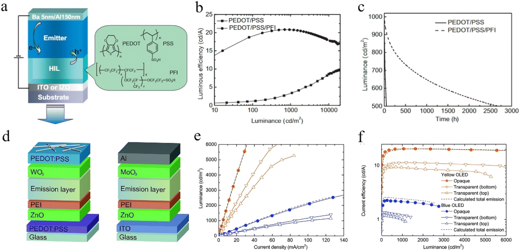 | ||
| Fig. 1 (a) PLED device structure and the chemical structures of the components of conducting polymer compositions used for HILs. Device luminous efficiency and device lifetime: (b) Luminous efficiency versus luminance and (c) device lifetime with an initial luminance of 1000 cd m−2 for the devices using PEDOT/PSS and PEDOT/PSS/PFI as a HIL.68 Copyright 2007 Wiley-VCH Verlag GmbH & Co. KGaA, Weinheim. (d) Device architectures of the all-solution processed TOLEDs comprising PEDOT:PSS bottom cathodes and PEDOT:PSS/AgNW top anodes and the opaque reference OLEDs. Optoelectronic characteristics of the yellow- and blue-emitting TOLEDs in comparison with those of the respective opaque reference devices. (e) Luminance vs. current density (L–J) and (f) current efficiency vs. luminance.70 Copyright 2015 The Royal Society of Chemistry. | ||
1,4,5,8,9,11-Hexaazatriphenylene hexacarbonitrile (HAT-CN) is a small molecule HIL material that is widely used in vacuum evaporation devices, especially used as a charge generation layer for laminated OLEDs. Lin et al. found that HAT-CN has strong selective solubility which makes it only dissolve in acetone but insoluble in commonly used solvents like chlorobenzene and toluene. By using acetone as the solvent of HATCN, a HIL layer with 4 nm thickness was fabricated, and the device performance was comparable to that of PEDOT:PSS OLEDs.59 For small molecule HIL materials, Dan et al. blended two HTL materials, mCP and TCTA, and accomplished the preparation of green solution-processed phosphorescent OLEDs (PHOLEDs).73 By mixing these two HTL materials, the drive voltage at 1000 cd m−2 was effectively reduced from 6.5 to 5.5 V. This hybrid strategy has successfully realized a novel type of hybrid material with better cavity, transport capacity and solubility resistance. Compared with the device with the single HIL of TCTA, the device with the combined HIL has a higher current efficiency (CE) and a lower turn-on voltage. As a result, the optimized device of the combined OLED showed a maximum CE and a power efficiency (PE) of 39.5 cd A−1 and 24.5 lm W−1, respectively.
Inorganic HIL materials. Inorganic HIL materials such as metal oxide, metal sulfide and some other inorganic materials are also noted for the preparation of solution-processed OLEDs. Metal oxide always refers to the transition metal oxide (TMO), which includes the commonly used MoO3,74,75 NiOx,76,77 WO3,78 and V2O579,80 and so on. As shown in Fig. 2a, these TMO HIL materials have a high value of ϕWF close to 7.0 eV, resulting in a deep conduction band (CB). In another word, its hole injection mechanism will be different from other HIL materials. To put it simply, the hole injection mechanism of TMO is that the HOMO electrons of the HTL will be extracted to the CB of TMO to realize an equivalent hole injection.81 There are two kinds of solution-processed TMOs, one is precursor solution and the other is nanoparticle dispersion. For the TMO precursor solution, researchers will choose different solvents for different solution-processed technologies. In general, a polar solvent such as isopropyl alcohol is chosen in order to achieve orthogonality with the solvent of the emitting layer (EML). MoO3 is a commonly used HIL material in vacuum evaporation OLEDs with a ϕWF value, CB and valence band (VB) of 6.7 eV, 6.9 eV and 9.7 eV, respectively. It has the advantages of low cost, strong hole injection ability and no corrosion to the ITO anode. Many studies have applied MoO3 in the solution OLED through different solution synthesis methods. Liu et al. proposed a solution method. They first dissolved powder MoO3 in ammonia water and then diluted it with deionized water. Finally, this kind of s-MoO3 thin film showed better hole injection performance and reduced exciton quenching, thus improving the performance of the device.74 Murase et al. preheated the MoO3 precursor solution in deionized water before spin-coating, after which a very uniform and unbroken film was obtained.82 By utilizing the sol–gel method, Girotto et al. dissolved MoO3 into H2O2 to form the MoO2(OH)(OOH) precursor solution.83 TMO is susceptible for the preparation environment and the value of ϕWF may be dramatically cut from about 7.0 eV to about 5.0 eV by the polluted air, which has been verified by the research studies of Irfan et al. and Hancox et al. of MoO384 and V2O5,76 respectively. Therefore, the value of ϕWF of solution-based TMO is always in the range of 5.3 to 5.7 eV. To repair the loss of ϕWF, Hammond et al. managed to increase the ϕWF value of MoO3 from 5.0 to 6.1 eV by combining high temperature treatment under a vacuum environment and oxygen plasma treatment.85
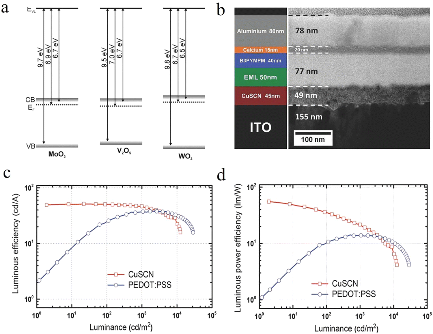 | ||
| Fig. 2 (a) CB minimum and VB maximum with respect to the vacuum levels of MoO3, V2O5 and WO3.81 Copyright 2012 Wiley-VCH Verlag GmbH & Co. KGaA, Weinheim. (b) TEM image of the focused ion beam (FIB)-milled cross-section of a complete CuSCN HIL/HTL OLED (right side), together with a schematic of its stack structure (left side). The comparison of the OLED characteristics of CuSCN and PEDOT:PSS HIL/HTL structures. (c) Luminous efficiency (cd A−1) versus luminance (cd m−2) characteristics and (d) luminous power efficiency (l m W−1) versus luminance (cd m−2) characteristics of PEDOT:PSS (circles) and CuSCN (squares) structures.47 Copyright 2014 Wiley-VCH Verlag GmbH & Co. KGaA, Weinheim. | ||
Copper thiocyanate (CuSCN) is a p-type semiconductor that is cheap and easy to be synthesized.47,86,87 TMOs and small molecule HAT-CN often require precise control for a few nanometers and an additional HTL which greatly limits their application prospect. But, for CuSCN, it has good air stability and a high hole mobility of 0.01–0.1 cm2 V−1 s−1. Moreover, CuSCN can withstand the erosion of various organic solvents, which makes it better for the fabrication of laminated OLEDs, and thus expands its application in OLEDs, OSCs and PSCs. Perumal et al. demonstrated a high-performance solution-processed green PHOLED by blending CuSCN HIL/HTL and the (PPy)2Ir(acac) EML.47 In their work, CuSCN-based devices showed a maximum luminance, CE and PE of over 10![[thin space (1/6-em)]](https://www.rsc.org/images/entities/char_2009.gif) 000 cd m−2, 50 cd A−1 and 55 lm W−1 (Fig. 2c and d).
000 cd m−2, 50 cd A−1 and 55 lm W−1 (Fig. 2c and d).
Organic EIL materials. At present, metal cathodes with relatively high ϕWF and good air stability are commonly used in OLEDs, but the high value of the LUMO is not conducive for electron injection. To obtain highly efficient electron-injection, alkali metals with low ϕWF should be used as cathodes. However, these metals are too active, resulting in poor stability and difficulty in solution processing. To solve this problem, recently, a great breakthrough has been made in water–alcohol-soluble interfacial EIL materials. Using water/alcohol as the solvent, the destruction of the organic layer can be effectively avoided. In general, organic functional layers are insoluble in water/alcohol polar solvents. These materials can be divided into conjugated and non-conjugated polymers according to their molecular framework.88
Based on the conjugated polymer, in 2004, Cao et al. first synthesized conjugated polymers poly[(9,9-bis(3′-(N,N-dimethylamino)-propyl)-2,7-fluorene)-alt-2,7-(9,9-dioctylfluorene)] (PFN) and used it as the EIL for PLEDs. They also found that even using a metal with high ϕWF as the cathode could obtain high-performance solution-processed OLEDs.89,90 Since then, more and more research groups have carried out a series of modifications on the conjugated polymer PFN. For instance, poly[9,9-bis(60-(N,N-diethylamino)hexyl)-fluorene-alt-9,9-bis(3-ethyl-(oxetane-3-ethyloxy)-hexyl)-fluorene] (PFN-OX)91–93 and poly[9,9-bis(6-(N,N-diethylamino)propyl)fluorene-alt-9,9-bis(hex-5-en-1-yl)-fluorene] (PFN-V)94 with a crosslinking characteristic can achieve highly efficient inverted OLEDs, while poly[(9,9-bis(3′-(N,N-dimethylamino)propyl)-2,7-fluorene)-alt-5,5′-bis(2,2′-thiophene)-2,6-naphthalene-1,4,5,8-tetracaboxylic-N,N′-di(2-ethylhexyl)imide] (PFN-2TNDI)95,96 with a high electron mobility can reduce the sensitivity of the thickness of the EIL. WOLEDs with an inverted structure prepared by solution methods have attracted more and more attention. However, for the ITO cathode and the metal anode, if ZnO is used as the electron transport layer (ETL), the charge injection potential barrier will be too high. To overcome this issue, Zhang et al. used modified PFN-OX, a novel cross-linked polymer, as the EIL modification layer. The CE and PE of their prepared devices were 18.8 cd A−1 and 6.7 lm W−1, respectively (Fig. 3).91 Hwang et al. used cross-linked poly(FA90-co-BFA10) as the HIL, a solution-processable red phosphorescent OLED that exhibited a low turn-on voltage of 3.5 V, a reasonably high CE of 16.6 cd A−1, and an EQE of 12.5%, all of which are superior to the corresponding reference device using PEDOT:PSS as the HIL.97 Xue et al. were successful in preparing high-efficiency polymer WOLEDs by using three small molecule luminescent materials of red, green and blue.98 In this work, they used poly[9,9-bis(2-(2-(2-diethanolamino ethoxy)ethoxy)ethyl) fluorene] (PF-OH) as the EIL to increase the CE of the original device from 9.2 cd A−1 to 20.7 cd A−1 and the turn-on voltage was reduced from 6.7 V to 4.5 V. Moreover, they further blended Li2CO3 into the conjugated polymer PF-OH to build up an n-type EIL/ETL. Consequently, their prepared Ph-WOLED has exhibited an optimal CE and PE of 36.1 cd A−1 and 23.4 lm W−1, respectively. With respect to non-conjugated polymer EIL materials, in 2012, polyethylenimine ethoxylated (PEIE) and PEI were reported by Bernard et al. Compared with the conjugated polymer like PFN, it is necessary for them to pay more attention to the thickness control of the EIL but also this class of materials can introduce a stronger interface dipole, which can effectively reduce the ϕWF of the electrode and achieve more efficient electron-injection.41
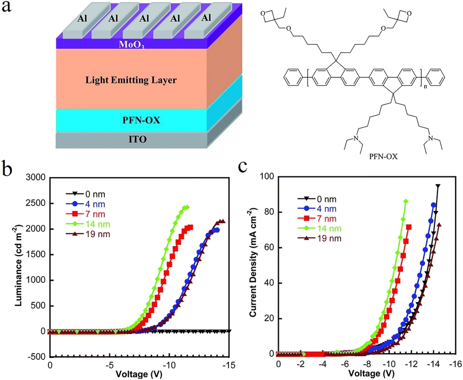 | ||
| Fig. 3 (a) The device configuration of the inverted OLED and the chemical structures of PFN-OX and light emitting layer materials used in this study. (b) L–V and (c) J–V curves of blue light devices with different thicknesses of the PFN-OX interlayer.91 Copyright 2014 The Royal Society of Chemistry. | ||
Inorganic EIL materials. Compared with organic EIL materials, inorganic EIL materials show better stability and resistance to solvent erosion. In particular, for ZnO EIL, it is widely used in all-solution-processed OSCs and QLEDs.99,100 As mentioned above, when using ZnO as the EIL material in OLEDs, it can provide effective electron-injection only when the EML material has a deep LUMO. However, the LUMO energy level of most organic materials is always located in the range of −2.0 to −3.0 eV, which greatly limits the application of inorganic EIL materials in the OLED field. Taking the aforementioned issue into consideration, Cao et al. prepared highly efficient all-solution-processed OLEDs by combining the merit of more effective electron-injection in the organic EIL with the merit of being erosion-proof in the inorganic EIL. In their work, they have designed a novel organic/inorganic hybrid PFN-OX/ZnO EIL. In contrast with the non-hybrid PFN-OX EIL, the hybrid EIL device demonstrated higher efficiency and lower switch-on voltage when using silver paste as the cathode (Fig. 4).101 They also designed a “solvent detector” so as to quantitatively study the ability of the resist dissolution of the PFN-OX/ZnO EIL. The change of the transverse conductivity of PEDOT:PSS is used to judge whether the solvent has been penetrated by the upper layer. As a result, the transverse conductivity of PEDOT:PSS did not change, indicating that the hybrid PFN-OX/ZnO EIL can completely prevent the downward infiltration of triethylene glycol monomethyl ether (TGME) solvent, and thus effectively protect the organic EML. Finally, the prepared all-solution-processed blue emission device can reach a maximum CE of 2.5 cd A−1 at 6.4 V. Besides, there are many other promising inorganic EIL materials, such as cesium stearate102 and Cs2CO3,103,104 which can also be converted for the solution-processed EIL.
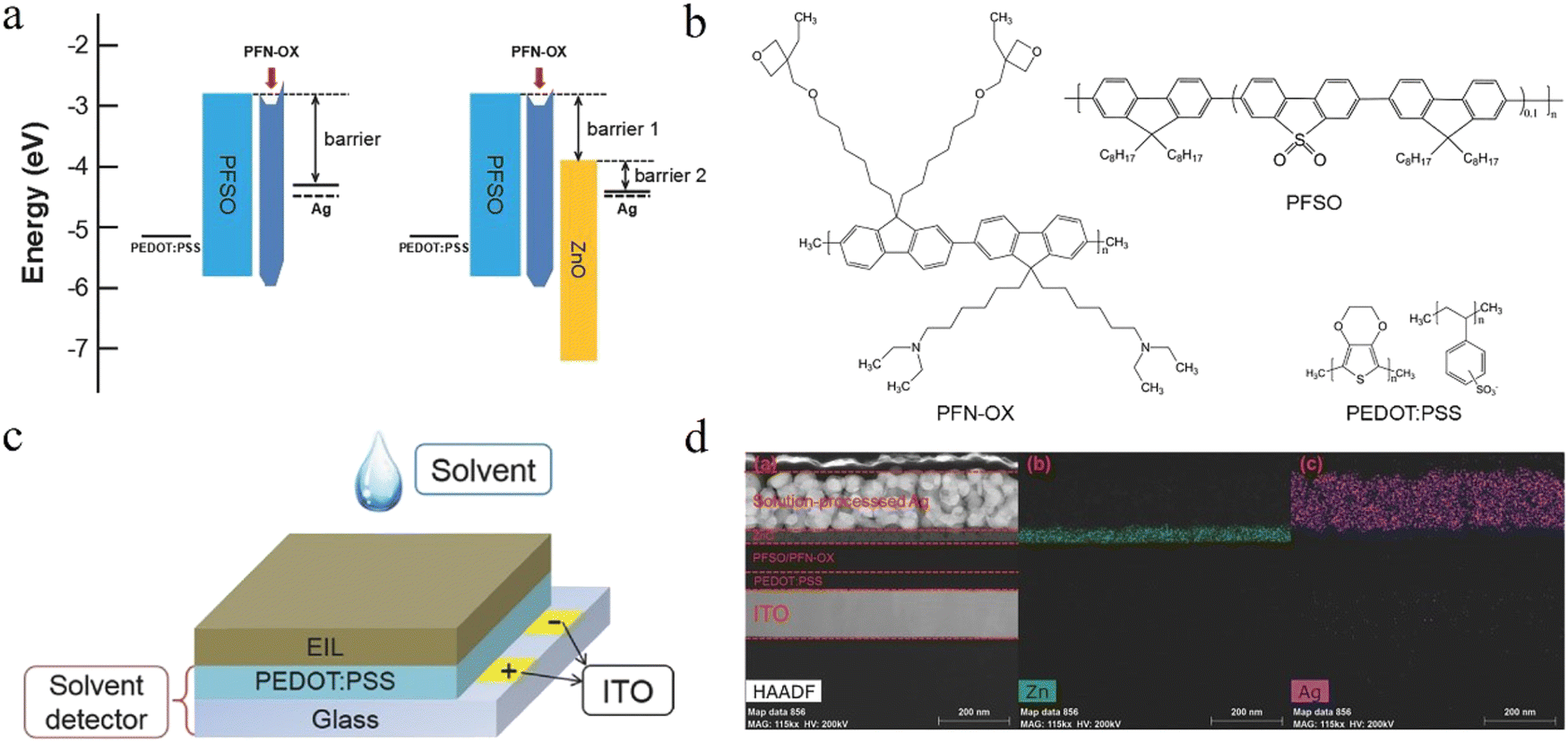 | ||
| Fig. 4 (a) Energy level diagrams of the device. (b) Chemical structures of PFSO, PFN-OX, and PEDOT:PSS. (c) Schematic illustration of the “solvent detector.” (d) EDS map of the all-solution-processed OLED.101 Copyright 2018 Wiley-VCH Verlag GmbH & Co. KGaA, Weinheim. | ||
2.3 Transport layer
Another way to obtain stable films is to use starburst hole transport materials based on the TDATA and TDAPB families. For example, m-MTDATA and 2-TNATA have been used as HTL materials in many works and played an important role.111 m-MTDATA and its analogs have extremely low solid-state ionization sites (5.0–5.1 eV) and are reversibly anodized to generate stable cationic radicals.112 In addition, spin-coated amorphous films using this material have very good film quality.
Compared with TDATA, TDAPB is resistant to crystallization due to its high Tg and steric hindrance by the four central phenyl groups. At the same time, because of its high solubility, it is more convenient for solution preparation. Wehrmann et al. added TDAPB between the HIL and EML.62 By comparing the device characteristics and working life with the device without TDAPB, it was proved that the addition of TDAPB can not only prepare high-efficiency devices, but also prolong device lifetimes.
Chae et al. used TCTA with good film formation and solubility as the HTL material for green Ph-OLEDs.105 TCTA can be prepared by both spin coating and vacuum evaporation, but the surface roughness of the TCTA films obtained by the two methods is different, which is mainly due to solvent evaporation during spin coating. TCTA can form a good amorphous film mainly due to its three-dimensional structure. TCTA has two coplanar carbazole units, one of which is perpendicular to the plane containing the two carbazole units, which is conducive to the formation of amorphous molecular packing. Ultimately, they successfully fabricated green PHOLEDs with efficiencies of 33.7 cd A−1 and 19.6 lm W−1, respectively.
Periasamy et al. designed and synthesized two HTL materials, DHABS and DPABS;113 their HOMOs are comparable to the widely used TPD, although the device performance based on these two HTL materials is not as good as the TPD-based device, but also provides us with new ideas. Kido et al. used a-NPD as the HTL material and 10 wt% TBPAH doped with DFPA2 as the hole injection buffer layer,114 finally obtained a device with low Von and high PE. Taniguchi et al. designed and synthesized a new thermally stable HTL material T-Caz,115 which has an extremely high Tg of 250 °C. Based on this HTL material, a green device with a maximum brightness of 10300 cd m−2 was finally prepared.
A new small molecule thermally cross-linked material PbV was synthesized by Ha et al. This newly synthesized HTM has almost no pinholes after the cross-linking reaction and can form very uniform films. The corresponding red phosphorescent OLED showed a CE of about 16.7 cd A−1 and an EQE of 12.4%.116 Thermal cross-linked materials E-TPD were designed and synthesized by Peng et al. The corresponding solution-processed green phosphorescent OLED obtained excellent performance with a Von of 3.3 V, a CEmax of 60.74 cd A−1, and an EQEmax of 17.33%.117
Currently, PBD is commonly used in the ETL, but PBD also has defects. For example, it is a crystalline material, and it is also very easy to crystallize at room temperature. Therefore, in order to obtain stable amorphous ETL materials, scientists have also synthesized PBD-based spiro, branched derivatives and starburst dendrimers, which are widely used in OLEDs.
Besides PBD, triazole and benzimidazole derivatives are also commonly used ETL materials, such as TPBI and TAZ, which can not only facilitate electron transport but also better block excitons. TPBi also has the characteristics of high solubility in alcohol solvents, which also makes TPBi play an important role in the preparation of OLEDs by solution methods.118 Taniguchi et al. synthesized novel amorphous ETL materials phenoxy-TPBi with benzimidazole,119 both of which have high Tg (= 108 to 110 °C) and thermal stability, and are easily soluble in common organic solvents such as acetone and tetrahydrofuran. Devices based on these two ETL materials show no emission phenomenon, but carrier transport properties can be observed (400 mA cm−2).
In addition to the above, pyridine-based derivatives are also outstanding among ETL materials for OLEDs.120 The reported electron mobility of TMPPB is as high as 7.9 × 10⁻³ cm2 V−1 s−1, which is also very shocking data.121 Petty et al. developed a series of ETL materials based on two oxadiazole derivatives and three oxadiazole novel-containing pyridine units. They mixed these materials with MEH-PPV and carefully studied the effect of ETL thickness and annealing on the device. Their results showed that oxadiazole molecules containing pyridine units were more stable than those containing benzene rings alone.
Although many amorphous ETL materials have good solubility, they are often used in solution preparation to prepare smooth, flat and stable films. However, in most of the work, in order to prevent the light-emitting layer from being dissolved, the vacuum deposition method is chosen to prepare the ETL. There is still a long way to go to study ETL materials in order to simplify the process of solution preparation, reduce the cost of device preparation and accelerate the commercialization of OLEDs.
2.4 Emitting layer
Printed OLED emitting materials mainly include organic small molecule materials (phosphorescent materials, fluorescent materials, and TADF materials) and polymer materials, which play a very important role in the performance of devices. Generally, if the small molecule emitting materials used in the traditional evaporation process are directly applied to the printing process, the performance of the device will be seriously affected due to its low solubility and poor film-forming effect. The development of new printed OLED emitting materials not only needs to pay attention to their luminescence efficiency, film-forming properties, stability, color purity and cost, but also needs to focus on the materials themselves to match the printing process.From the development history of emitting materials, the first generation of luminescent materials is fluorescent molecules represented by Alq3, which are gradually replaced (<25%) due to the limitation of an internal quantum efficiency (Fig. 5a).122–125 These devices are generally inefficient and cannot meet the application requirements.
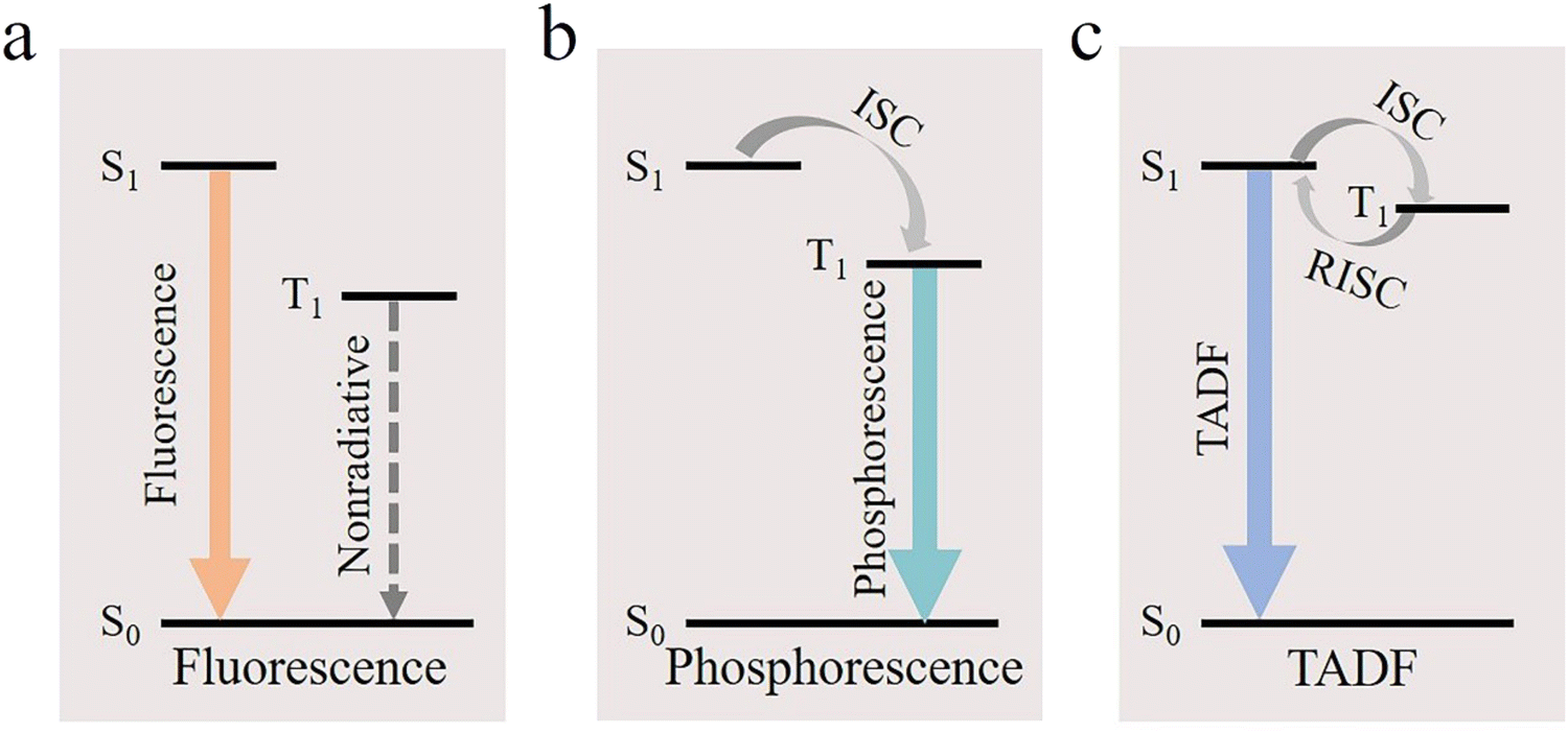 | ||
| Fig. 5 Mechanism of (a) fluorescent, (b) phosphorescent, and (c) TADF materials. | ||
To break through this limitation, PHOLEDs with an internal quantum efficiency of nearly 100% have been developed (Fig. 5b).126–129 Phosphorescent materials are mainly divided into pure organic phosphorescent materials and complex phosphorescent materials with heavy metals as the core. Pure organic phosphorescent materials have high flexibility, low cost, environmental protection and other application potential, but their performance is still poor. Therefore, the OLED technology of complex phosphorescent materials is more popular at present. In order to achieve appropriate solubility and inhibit the self-quenching effect and triplet–triplet annihilation effect, small molecule phosphorescent materials usually obtain high quantum efficiency by matching with the polymer host or doping hole transport materials. In 2019, Xing et al. investigated the inkjet-printed OLEDs of Ir(mppy)3 with a mixture of m-MTDATA and TPBi as the co-host and obtained a maximum brightness of 13240 cd m−2.130 In 2020, Mu et al. successfully prepared a binary phosphorescent small molecule material based on Ir(MDQ)2(acac). The maximum current efficiency produced by the ink-jet printed PHOLED was 17.89 cd A−1.131 Zhang et al. reported a doping method of blending a small molecule phosphorescent material with a transmission material. The maximum brightness of the prepared green phosphorescent device reached 40320 cd m−2, the maximum current efficiency reached 40.9 cd A−1, and color coordinates are (0.300, 0.630).132 Dpan-5bzac, a bipolar transport material with high triplet energy, was mixed with hole transport materials MCP and TCTA as the main body of ternary blending. Combined with the typical iridium coordinated phosphorescent material IR(PPy)2acac, the excellent miscibility and ordered structure of the light-emitting layer were realized, and the transport balance of carriers was enhanced.
In recent years, thermally activated delayed fluorescence (TADF) has also been used to improve the efficiency of OLEDs. In the TADF mechanism, the triplet state is converted to the singlet state by reverse intersystem crossing (RISC) to obtain 100% of excitons generated by electrical excitation in the device (Fig. 5c).133–137 In 2016, Verma et al. realized the TADF-OLED by ink-jet printing for the first time. The CE of the OLED reached 45 cd A−1, and the EQE was 13.9% ± 1.9%.138 In 2019, Amruth et al. investigated and optimized the TADF material tBuG2TAZ in printed OLEDs. The prepared devices realized a maximum CE of 18.0 cd A−1 and a maximum brightness of 6900 cd m−2.139 OLEDs with TADF as the main material have many advantages, such as low driving voltage, high efficiency, long lifetime and low efficiency roll-off. However, due to its poor solubility, there are still many challenges in the preparation of inkjet printing.
882 cd m−2, and the color coordinates are (0.160, 0.150).140 Zhang et al. embedded a small amount of 2,5-dimethyl-1,4-p-phenylene units in the polyfluorene skeleton to synthesize PFDPN. Structurally, PFDPN inserts flexible units into the main chain of polyfluorene, resulting in a disordered conformation during film formation, increasing its radiation attenuation rate, and finally improving the electrical and optical properties of the device.
Similar to TADF small molecular materials, the design of TADF polymer materials also requires the construction of a small enough energy gap to achieve a fast RISC process. Shao et al. reported a molecular design strategy of the non-conjugated TADF blue photopolymer for solution treatment, and synthesized the polymer P-Ac-TRZ.141 The spatial gap between polyethylene and the acceptor is high, so that the side chain of polyethylene can not only be separated from the acceptor, but also the side chain of the acceptor can be separated, so that the side chain of polyethylene can be separated from the acceptor. Finally, the EQEmax of the device made of the polymer material reached 12.10%, and the color coordinates are (0.176, 0.269). In addition, dendritic macromolecular materials, which integrate the advantages of small molecular materials and polymer materials, have also attracted extensive attention as luminescent materials for printed OLEDs. The unique dendritic branch structure not only forms a certain steric hindrance, but also makes the material soluble and amorphous and has good thermal stability through flexible modification.142
3. Device structure
At present, in most vacuum-deposited OLEDs, the multi-layer structure is more beneficial to realize high efficiency and long lifetime. This is mainly because it can more precisely control the injection and transport of carriers, the formation and distribution of excitons, and the energy transfer between the host and the object.143 At the same time, since each layer of vacuum-deposited OLEDs is sequentially deposited under vacuum, the film coverage of each layer is uniform and flat, and the function of other layers will not be affected. Compared with vacuum-deposited OLEDs, solution-processed OLEDs are difficult to prepare multi-layer structures due to the possible problems of interdiffusion and compatibility between layers. The performance of solution-processed OLEDs will be even better with using cross-linked materials and orthogonal solvent strategies.144–146 Although some scientists have been studying and synthesizing new functional materials in order to realize ideal multi-layer solution-processed OLEDs,147 more work has been focused on exploring solution-processed OLEDs with a simpler structure or employing a hybrid procedure of the solution process and vacuum deposition.148 In this hybrid structure, the EML is generally prepared by solution methods, and the electron buffer layer (EBL) and the ETL are prepared by the vacuum deposition method. This method is suitable for PHOLEDs, which can prolong the lifetime of triplet excitons. Excellent performance can be achieved by confining triplet excitons in the EML via adding the EBL.To meet the goal of commercialization, reducing the preparation cost is the top priority of solution-processed OLEDs, but at the same time, it is necessary to ensure that the efficiency and life of devices are not affected. Therefore, the solution process needs to meet the following requirements: (1) use efficient, low-cost, and stable materials for each layer as much as possible, and each layer cannot interfere with each other, which can synergistically extend the device life of solution-processed OLEDs. (2) Each layer should be prepared by solution methods as much as possible, using orthogonal solvents as far as possible and ensure that the film formation of each layer is smooth and uniform at the same time. (3) The device structure is as simple as possible, thereby reducing production costs and processes. (4) The energy level matching material is used to reduce the energy level barrier, which is beneficial to charge carrier injection and transport.
3.1 Basic device structure
Firstly, some typical device structures of solution-processed OLEDs and the corresponding fabrication methods are introduced. As shown in Fig. 6a, it is the simplest device structure of solution-processed OLEDs, consisting of only two films prepared by solution methods. PEDOT:PSS is commonly used as the HIL. For the cathode, different metal electrodes are also used in different works. Wang et al. successfully prepared a device with a brightness of 11900cdm−2 using Ca/Al as the electrode.149 Cao et al.150 and Kido et al.151 used Ba/Al and Mg:Ag to prepare different devices, respectively. The devices with the simplest structure have made a great contribution to the industrial preparation of large-scale OLEDs in terms of reducing the cost and the preparation process,152,153 and also promoted the large-scale manufacturing of solution-processed OLEDs. However, due to the small number of layers, the optimization of each layer is particularly important. Wong et al. used low-conductivity PEDOT:PSS as the anode buffer layer of the device, and further optimized the EML, finally obtained a device with an EQEmax of 28.8% and a CEmax exceeding 60 cd A−1.154 Instead of using the traditional two-layer cathode (BaF2/Al and Ba/Al), chin et al. used a novel three-layer cathode (BaF2/Ca/Al) which greatly improved the lifetime of the device.155 At the same time, the influence of the thickness of BaF2 on the device performance was studied. As shown in Fig. 7, when the thickness of BaF2 is less than 3 nm, Ca will be in direct contact with the EML, which will cause the luminescence quenching of Ca, and will also reduce the lifetime of the device. In contrast, if a BaF2 layer of 3–8 nm is used, the direct contact of Ca with the EML can be avoided. There will be a CaF2 layer or a mixed layer of BaF2 and CaF2, which is beneficial to the injection and transport of carriers. In addition, there are also some works to add some buffer layers between the EML and the cathode to prolong the lifetime of the device during operation.156–158
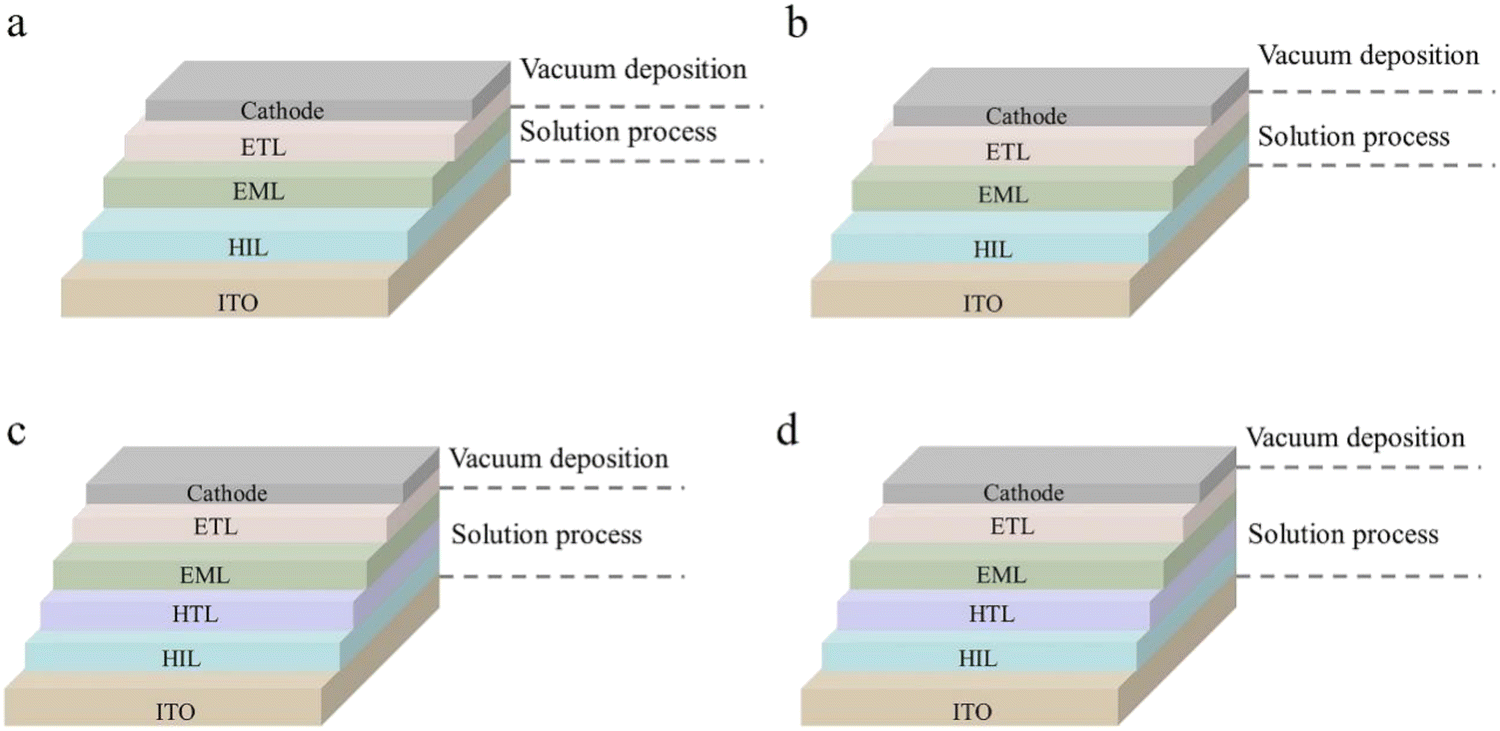 | ||
| Fig. 6 Basic device structures and processing method of solution-processed OLEDs with (a) solution-processed HIL/EML, (b) solution-processed HIL/EML/ETL, (c) HIL/HTL/EML, and (d) HIL/HTL/EML/ETL, respectively. | ||
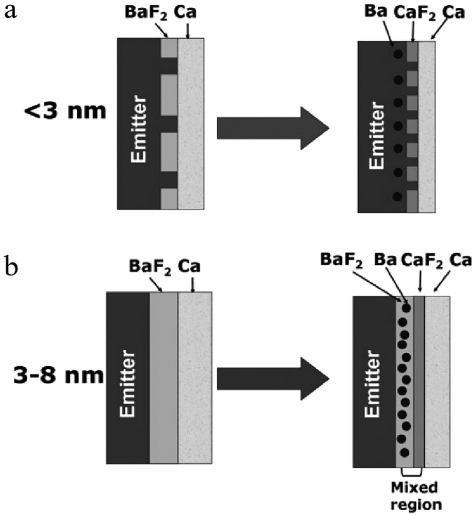 | ||
| Fig. 7 Schematic diagrams of the contact between the cathode (BaF2/Ca/Al) and the emitter for (a) a thin BaF2 layer with a thickness less than 3 nm, and (b) a BaF2 layer with a thickness of 3–8 nm.155 Copyright 2009 Wiley-VCH Verlag GmbH & Co. KGaA, Weinheim. | ||
As shown in Fig. 6b, a vacuum-deposited ETL is added between the EML and the cathode, which can promote the injection and transmission of electrons. Meanwhile, the use of an ETL with a suitable energy level can confine the excitons in the EML,159 which can increase the utilization of excitons, thereby improving the efficiency of solution-processed OLEDs. Wang et al. prepared high-efficiency solution-processed deep-blue and white OLEDs with FIr6 as the blue material and PVK as the host.159 In addition, they added an interface layer with a higher triplet energy level between the EML and the ETL, which can effectively inhibit the transfer of excitons from the EML to the ETL, thereby reducing the energy loss of excitons. It can also improve the performance and prolong the work lifetime of devices. Finally, the deep-blue OLED achieved an EQE, a CE and a PE of 16.1%, 31.5 cd A−1 and 15.1 lm W−1, respectively. Besides, white OLEDs achieved a high total EQE and a PE of 28.0% and 38.4 lm W−1, respectively. This work further demonstrated the importance of reducing triplet exciton loss at the interfaces. Similarly, Wang et al. also used a high-energy-level blue phosphorescent material FIr-p-OC8 in the EML to prepare solution-processed WOLEDs with an efficiency comparable to that of fluorescent tubes.160 FIr-p-OC8 not only achieved efficient blue emission, but also enhanced the HOMO/LUMO levels to match the dendritic host H2 well. At the same time, as shown in Fig. 8, the direct formation of excitons on the blue phosphorescent material can reduce the turn-on voltage and improve the power efficiency. The PEmax of WOLEDs based on FIr-p-OC8 reached 68.5 lm W−1, which decreases slightly to 47.0 lm W−1 at a brightness of 1000 cd m−2. By introducing light extraction technology, the efficiency can be further improved to 96.3 lm W−1 at a brightness of 1000 cd m−2. Their results can compete with commercial fluorescent tubes with a good level of reference.
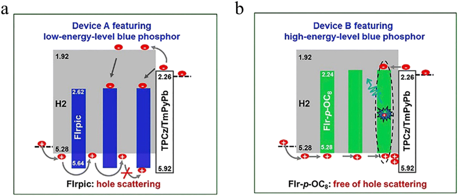 | ||
| Fig. 8 Effect analysis of hole scattering. (a) Working mechanism of the FIrpic-based blue device. (b) Working mechanism of the FIr-p-OC8-based blue device.160 Copyright 2018 Elsevier. | ||
In OLEDs, the optimization of the transport layer is extremely important because the mobilities of electrons and holes in the corresponding transport layers differ by 1–2 orders of magnitude. Although the commonly used PEDOT:PSS has been widely used,161–163 its shortcomings cannot be ignored. For example, PEDOT will corrode the ITO substrate, resulting in the diffusion of the anode metal to the EML,68 which will seriously affect the performance of the device. In addition, the energy level gap will also weaken the hole injection ability.67,164 To address these issues, the HTL can be further added to the HIL and the EML, as shown in Fig. 6c. During operation, layer-to-layer interactions should also be avoided. Chen et al. just considered that exciton quenching at the interface between PEDOT:PSS and EML would affect the efficiency and lifetime of the device,147 so they introduced a cross-linkable HTL material Oxe-DCDPA, achieved solution-processed green and bluish-green OLEDs with efficiencies of 26.1%/94.8 cd A−1 and 24.0%/74.0 cd A−1, respectively. By further adding another material (X-DCDPA) and Oxe-DCDPA to form a double HTL structure, green and bluish-green OLEDs with efficiencies of 30.8%/111.9 cd A−1 and 27.2%/83.8 cd A−1, respectively, were finally obtained.
The structure shown in Fig. 6d is the device structure prepared by the solution method except the anode and the cathode. At present, many works using this structure have also achieved good results. Wang et al. successfully fabricated a multi-layer green OLED with an EQE of 21.2% and a CE of 68.4 cd A−1 by the layer-by-layer solution method of orthogonal solvents using the self-host dendrimers as non-EML materials.146 The efficiency of the device is comparable to that of the doped device, and it also avoided the problem of layer-to-layer dissolution, which is also beneficial for the reproducibility of the experiment. Similarly, Kido et al. demonstrated that small host molecules based on covalent dimerization or trimerization instead of polymerization were sufficiently resistant to the alcohol used to process the upper layer under solvent resistance tests for small host molecules,165 thereby preparing a series of blue, green and white high-efficiency solution-processed multilayer OLEDs with record PEmax of 36, 52 and 34 lm W−1 at 100 cd m−2, respectively. Their work also showed that the composition at the interface of the solution-processed layer is a key factor in determining device performance.
In addition to the above-mentioned cases that only the functional layers were processed by the solution method, the devices can be fabricated by solution methods for all functional layers including electrodes. This kind of all-solution structure is expected to further reduce the preparation cost, and the main challenge is to realize the solution preparation of the injection layer/electrode interface. Cao et al. achieved all-solution preparation by inkjet printing nanoscale silver particles on the buffer layer to uniformly fabricate the cathode using epoxy adhesive and a novel water-/alcohol-soluble conjugated polyfluorene polyelectrolyte PFNR2 as the buffer layer.166 A 1.5 inch display device is shown in Fig. 9a. The working principle of the buffer layer is that after the epoxy adhesive is cured, a stable three-dimensional copolymer network is formed by cross-linking, preventing the intrusion of organic solvents. Water-soluble conjugated polymers provide good film-forming ability, necessary electron injection ability, and the modulation of surface energy to match the printed cathode. The resulting 1.5 inch polymer light-emitting diode display was manufactured without any dead pixels. This process solved the problem of high vacuum for the thermal evaporation of the cathode and paved the way for the manufacture of the flat panel display in industry. In the following work, they combined the advantages of organic and inorganic EILs to prepare an all-solution-processed OLED with an efficiency of 2.1 cd A−1 using a novel hybrid EIL (PFN-OX/ZnO) and spin-coated silver nanoparticles as cathodes.101 This hybrid EIL not only exhibited better electron injection, but also retained the solvent resistance of inorganic EILs. In addition to using silver nanoparticles as electrodes to prepare solution-processed OLEDs, PEDOT:PSS/silver nanowires can also be used as the anode of solution inversion devices.70 Although these all-solution OLED devices have the potential to reduce production costs, the efficiency of the devices reported so far is relatively low, and there is no further research on stability; so there is still a long way to go to meet the market requirements.
 | ||
| Fig. 9 Device structures and photographs of monochrome and full-color displays. (a) Schematic of the full color structure. (b) Microscopic image of the back of the display. (c) Red, (d) blue and (e) green monochrome displays. (f) Full-color display with a microscopic image.166 Copyright 2013, Nature Publishing Group. | ||
3.2 Inverted hybrid device structure
Organic/inorganic hybrid structure refers to the mixture of an inorganic injection/transport layer and an organic EML. It is usually inverted, and the n-type metal oxide is deposited on ITO as an EIL/ETL, and electrons are transferred from the conduction band of the n-type metal oxide to the LUMO level of the EML. Finally, a high work function and stable metals (e.g., gold and platinum) are used as anodes.167 Commonly, a layer of metal oxide with a deep conduction band energy level is also deposited between the EML and the anode to increase the hole injection capability. The advantage of the hybrid structure is the use of stable injection/transport layers and the avoidance of reactive cathodes (e.g. Li/AL, Ba/Ag, Ca/Al), thus enhancing the lifetime of the device. At the same time, the structure is also simple, and a suitable injection layer is matched to improve the injection of carriers, which can better improve the efficiency of the device.In the inverted hybrid structure, expensive vacuum-evaporated transition metal oxides are usually used as the HIL/HTL, which is not cost-effective. The reason for not using the low-cost solution method to prepare transition metal oxide films is due to the various problems of solution method transition metal oxides: the film roughness is large, the film contains defects, the work function decreases, the precursor diffuses to the active layer, which degrades its performance, and the film takes a long time to form. Therefore, only a few literature studies demonstrate the all-solution-processed method for preparing the transport layer. For example, in 2012, the use of a hydrolyzed solution method instead of vacuum evaporation to prepare the HIL/HTL (V2O5) and the ETL (ZnO), respectively.168 However, this work did not tap the potential advantages of the hybrid structure in terms of the optoelectronic performance and lifetime of the device. The inverted hybrid structure is limited by transport materials, especially HIL/HTL materials, and cannot obtain high-quality thin films, which greatly limits its performance. In addition, due to the energy level matching, the inverted hybrid structure cannot make full use of most of the materials suitable for the upright structure, which leads to the inflexible membrane structure design. By breaking through the bottleneck of transmission materials and expanding the flexibility of the membrane structure design of inverted hybrid OLEDs, the organic/inorganic hybrid structure is expected to gain greater development space.
3.3 Tandem device structures
The tandem structure is a device structure in which multiple light-emitting units are connected in series through a connection layer. At very low currents, devices based on the tandem structure can achieve high brightness. Under the same current density, since the aging characteristics of the tandem OLED and the traditional single OLED are the same, and the initial brightness of the former is larger, the lifetime of the tandem OLED is longer than that of the traditional OLED under the same initial brightness. In addition, tandem OLEDs are also characterized by operating the voltage and current efficiency proportional to the number of tandem cells, but the PE does not increase.Generally, more than 10 functional layers can be prepared by vacuum evaporation between the anode and the cathode of a series device with two luminescent units. However, due to the limitation of solvent orthogonality, the preparation of these functional layers by solution methods is a great challenge. In 2014, inverted OLEDs were reported to be prepared by a solution method; WO3/PEDOT:PSS/ZnO/PEI was used as the charge generation layer to connect two polymer light-emitting units in series as shown in Fig. 10a, and enhanced optoelectronics performance was obtained.169 Next, Kido's team demonstrated a positive series OLED, where phosphomolybdate hydrate (PMA)/TFB is used as a charge generating layer and two polymer luminescent units are connected in series, as shown in Fig. 10b.170 After this, they replaced the polymer material with a higher-efficient small-molecule material, and used PEDOT:PSS/neutral PEDOT:PSS as the conductive connection layer to prepare a solution-processed phosphorescent tandem OLED as shown in Fig. 10c.69 Finally, the green tandem OLED achieved a CE of 94 cd A−1 and a PE of 18.6 lm W−1, and the tandem WOLED achieved a CE of 69 cd A−1 and a PE of 14.1 lm W−1.
 | ||
| Fig. 10 Solution-processed OLEDs. (a) Inverted tandem OLED.169 Copyright 2014 Wiley-VCH Verlag GmbH & Co. KGaA, Weinheim. (b) Positive tandem OLED170 (Copyright 2014 Wiley-VCH Verlag GmbH & Co. KGaA, Weinheim) and (c) phosphorescent tandem OLED.69 Copyright 2015 Wiley-VCH Verlag GmbH & Co. KGaA, Weinheim. | ||
It can be seen from the above examples that the CE of the series structure is relatively high and the PE needs to be further improved. At the same time, it can also be concluded that the tandem structure of the solution method is more complicated, which increases the cost of device production.
3.4 Critical problems
Despite the above discussion about the structure of solution-processed OLEDs, solution-processed OLEDs also face morphological challenges. For solution-processed OLED systems composed of multiple components, such as polymer–small molecule mixed systems and polymer–polymer mixed systems, phase separation is difficult to avoid in the operation of devices,171,172 which will seriously affect various performance parameters of devices (such as efficiency, brightness, and lifetime). In order to solve these problems as much as possible, the use of solvents or mixtures of solvents with a special polarity solvent strategy is conducive to the construction of uniformly dispersed multi-component films.173,174Compared with the devices of the evaporation method, the quality control of the film forming process of the solution method is difficult to maintain. The molecular orientation is chaotic, the interface fluctuation is large, and the thickness of the same film is not uniform, which has a certain impact on the interface contact and carrier transmission of the liquid method film.175–183 To date, there are no general guidelines that are good at assessing and avoiding morphology-related problems in solution-processed OLEDs. In order to develop high performance solution-processed OLEDs, these problems should be carefully studied and appropriately solved.
4. Printing display technology
Solution-based printed OLED technology has recently attracted much attention from the display–screen industry. The display companies such as Samsung Display and LG Display hold several patents of the key technologies in solution-processed OLEDs. Compared with solution-processed OLEDs, currently, the most mature and reliable vacuum-deposited OLED technology with the highest technical index also has its demerits, such as high preparation cost, low material utilization rate and an inaccurate doping ratio of organic materials.9,148,184,187–189 Because of the huge potential of solution-processed OLED technology in large area and flexible device fabrication, it has the possibility to make the production and preparation of OLEDs as convenient as printing books in the future. Considering this superiority, it is critical to find a new method to replace vacuum-deposited technology. Printed OLED technology is a method to prepare thin films for OLEDs by using solution which is dissolved in organic solvents or other solvents. It always contains spin-coating, ink-jet printing and screen printing methods.190–192 In addition, the concentration and doping ratio of materials for solution-processed methods can be precisely adjusted, even with a low doping concentration. Here, we will introduce some representative solution-based methods and their applications for OLEDs in detail.4.1 Spin-coating
Spin-coating and evaporation are both main techniques for thin film deposition which are frequently used in laboratory and industrial electronic device fabrication. Fig. 11a shows a schematic diagram of the spin-coating process.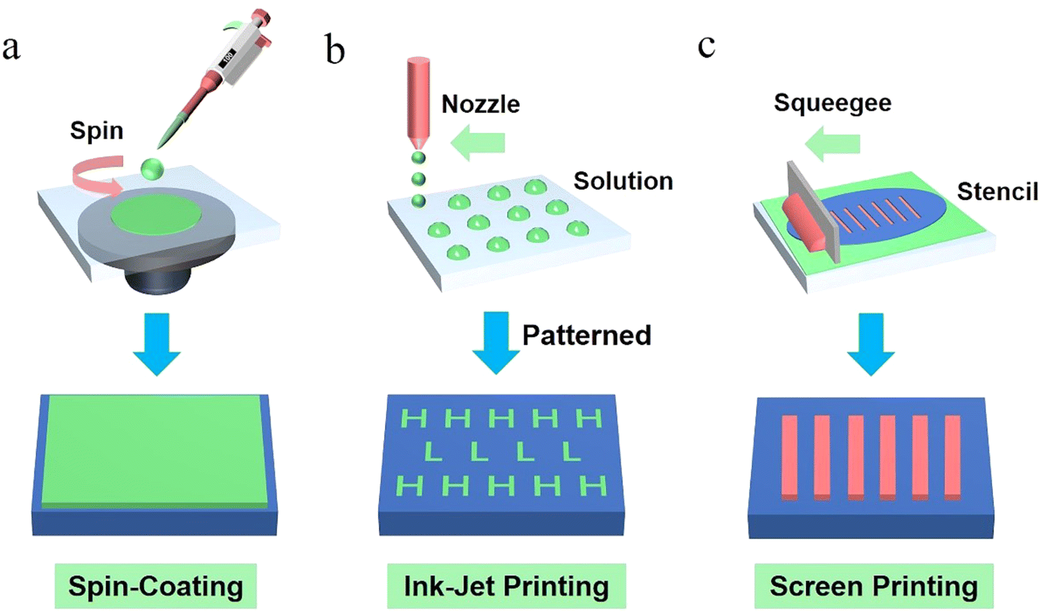 | ||
| Fig. 11 The common methods for solution-processed OLEDs: (a) spin-coating, (b) ink-jet printing and (c) screen printing. | ||
The so-called spin-coating method is using a vacuum pump to firmly absorb the substrate layer on the vacuum port, and then the prepared solution is dropped on the substrate. By utilizing centrifugation, the wet film will be formed by a given rotation speed, acceleration and time. Next, the wet film is transferred to a heating plate for annealing, with the aim of drying the solvent in the solution and further obtaining a dense smooth film. In the preparation process of spin-coating, the morphology of the film is also related to other conditions, such as solvent atmosphere in the glove box, the concentration of solution, humidity and oxygen conditions. And these factors can be adjusted to optimize device performance.193 In 1990, Burroughes et al. from Cambridge University synthesized poly(p-phenylene vinylene), a polymer with excellent air stability, and realized the preparation of OLEDs by the spin-coating method for the first time,9 thus setting off a great wave of solution-processed OLEDs.
In recent years, OLED fabrication by the spin-coating method also has made great breakthroughs. In terms of the luminescent layer, Sree et al. designed three phosphorescent iridium(III) complexes in 2018. The Ir 1 complex prepared by the spin-coating method achieved an EQE of 24.22%, and the corresponding CE reached 92.44 cd A−1. Moreover, when the brightness is 10000 cd A−1, it can still maintain 22.91% EQE, showing a low efficiency roll-off.194 In addition, TADF, as the third generation emitter of OLEDs, has also made ground-breaking achievements in the spin-coating method. As mentioned above, TADF materials prepared by the solution method can be divided into three types, containing a polymer, a small molecule and a dendritic molecule. In the context of fewer reports on polymer TADF materials, Ren et al. introduced styrene as a copolymer into the 2-(10H-phenothiazin-10-yl)dibenzothiophene-S,S-dioxide TADF material in 2016. By controlling the ratio of the TADF unit and styrene unit, an optimal EQE of 20.1% can be obtained for OLEDs by the spin-coating method at a unit ratio of 37%:63%(Copo1).195 In 2018, Colella et al. reported OLEDs based on the spin-coating method of small molecules 9-[2,8]-9-carbazole-[dibenzothiophene-S,S-dioxide]-carbazole (DCz-DBTO2) and 4,4′-cyclohexylidenebis[N,N-bis(4-methylphenyl)benzenamine] (TAPC).196 By changing the ratio of chlorobenzene and chloroform solvent, the film thickness and morphology of the small molecule excimer complex were controlled, and an optimal EQE of 8.9% was finally obtained. Besides, in 2019, Liu et al. synthesized four dendritic molecules 5CZBN-O-Cz, 5CZBN-O-2CZ, 5CZBN-CZ and 5CZBN-2CZ. Based on the spin-coating method, solution-processed OLEDs with a low turn-on voltage and high device efficiency were obtained, and the OLEDs based on the 5CZBN-2CZ TADF dendrimer even created more than 20% EQE which was comparable to vacuum evaporation devices.197 Lee et al. utilized the high triplet state energy level and good solution processability of tetraphenylsilane (with pyridine moieties) to prepare the electron transport layer by the spin-coating method, and obtained EQEs of 29% and 35.5% for green light and orange-red light solution-processed OLEDs, respectively.198
However, in terms of the thermal vacuum deposition process, the advantages of the spin-coating process are reflected in its convenient operation, precise control of doping ratio and large-area fabrication. Due to the operation properties of spin-coating, the waste of a large amount of solution is inevitable, and the utilization rate of the material tends to be low. Moreover, the single operation step also greatly limits the realization of patterned fabrication and full-color display, and makes it more suitable for the preparation of monochrome light-emitting diodes. Therefore, the following issues need to be solved urgently. Firstly, many small molecule materials hold a relatively low solubility in some common solvents, which hampers the formation of a complete film. Secondly, when multilayer devices are prepared by the spin-coating method, the solution in the upper layer may dissolve the solution in the former layer, resulting in an uneven morphology of the overall film, inhibiting the effect of each functional layer, and thus resulting in low device efficiency.199
Researchers have also put forward many measures to improve the above problems. In 2015, Cho et al. reported a method to change the molecular solubility and luminescence color by introducing F as electron withdrawing. Both the two blue synthesized TADF emitters can break the 20% EQE, which is comparable to the performance of the device prepared by the evaporation technique.200 In the preparation of full-solution OLEDs, Liu et al. replaced CB and CF, commonly used solvents of poly(9-vinlycarbazole) (PVK), with 1,4-dioxane orthogonal solvent in order to overcome the problem of the redispersion of solution. The use of orthogonal solvents not only did not destroy the luminescent layer, but also retained the integrity of each functional layer. Finally, the prepared blue QLED devices based on the PVK/TFB hole transport bilayer may achieve a 25-fold increase in luminous efficiency.201
4.2 Ink-jet printing
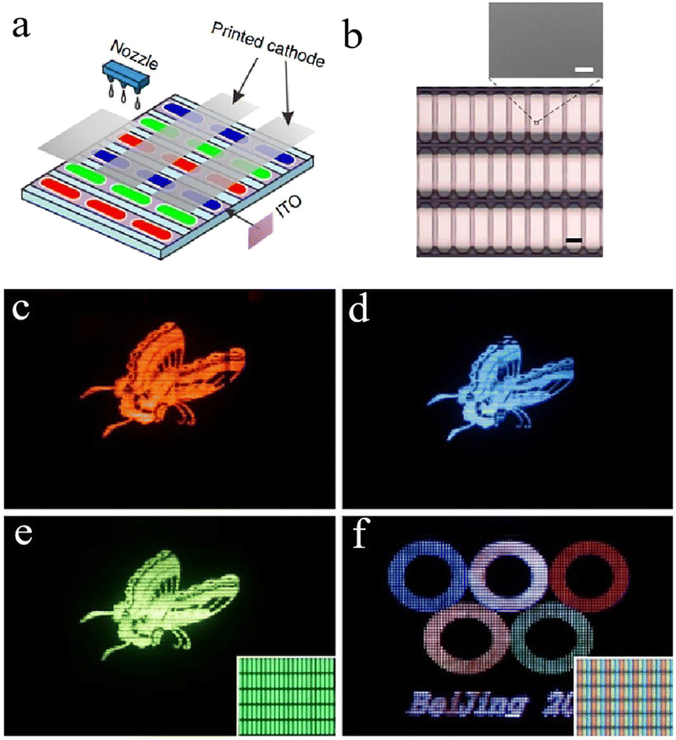
The spin-coating method has the advantages of simple operation and large-area preparation, while it is not satisfied with the high industrial demand with respect to the continuous improvement of the OLED manufacturing technique. As a result, printed electronics, which combine solution and advanced printing equipment, are becoming mainstream. Among them, ink-jet printing technology, as one of the most common printing technologies, can realize the preparation of patterned preparation, high-resolution display and full-color display. What's more, it can even overcome the material waste caused by the spin-coating method and achieve a high material utilization rate of more than 90%. Based on the above advantages, ink-jet printing is also considered to be the most suitable technology for preparing large-area OLED display panels.131Since the invention of the 19th century, inkjet printing has been widely used in biological chips and organic thin-film transistors.202,203 As a kind of printing technology, the biggest advantage of the inkjet printing is that it does not need to customize the expensive and complex templates in advance, and can write electronic patterns through computer control heads (Fig. 11b). In the ink-jet process, micrometer-diameter nozzles deposit small ink droplets onto the designed pattern at a rate of several thousand drops per second. The ink will go through four stages, namely, the ejection of ink droplets, the flight of ink droplets, the contact between ink droplets and the substrate, and the drying of films, which are affected by many factors.204,205 Generally, ink-jet printing equipment will have a number of nozzles, which are responsible for different colors of luminescent material inks and written into the corresponding groove, forming pixels.
First, the choice of solvent is critical in determining the stability of the process and printing behavior. In the ink-jet process, the ink should not block the nozzle, and it must have appropriate viscosity and surface tension to fully soak the designed pattern and improve the repeatability of the ink-jet process. Take polymer materials as an example, when choosing the solvent for the polymer ink, the frequently used volatile solvents in the spin-coating method, such as toluene and xylene, should be replaced by solvents with higher boiling points, such as trimethylbenzene and tetramethylbenzene. It is worth noting that polymer inks with high viscosity can greatly reduce device efficiency and hinder ink ejecting. In addition, when the surface tension of the ink droplet is too large, it will cause the phenomenon of droplet tail, which highly affects the quality of the pattern. Meanwhile, excessive soaking of the substrate will occur when the surface tension is too small. With reference to the aforementioned situation, it is very important to find a suitable ink.206
The key technology of ink-jet printing lies in the way of how to generate the droplets, which can be divided into continuous ink-jet (CIJ), drop-on-demand ink-jet (DOD) and electrospray technology.207 The schematic diagram of CIJ is shown in Fig. 12a. The ink is pressed out of the nozzle through the liquid column, presenting continuous and fractured ink droplets due to the “Rayleigh-plateau” instability. To precisely locate the ink at a point, the CIJ technique requires a charging device to form a charge on the droplets, followed by a recovery device to retrieve the remaining ink into a storage device. The diameter of CIJ droplets is generally about 100 μm, slightly larger than the diameter of the nozzle, the frequency of droplets is in the range of 20–60 kHz, and the droplet flight speed is up to 10–30 m s−1.
 | ||
| Fig. 12 Schematic diagrams of (a) continuous ink-jet and (b) piezoelectric drop-on-demand ink-jet. | ||
Because of the large diameter of droplets for CIJ technology, the problem of fine control needs to be overcome, and it is not conducive to the preparation of electronic devices. Moreover, CIJ technology includes a charging device, a deflector and a droplet recovery device, which is too complicated and expensive. The appearance of DOD ink-jet makes up for the deficiency of CIJ technology. First, DOD ink-jet works only when it is needed, resulting in significant cost savings. It can produce droplet sizes in the range of 20–50 μm, which makes it the most popular ink-jet technology in the field of micron electronic devices. According to different nozzles, DOD ink-jet can be divided into piezoelectric (Fig. 12b) and thermal foaming. Piezoelectric ink-jet printing is a technology that relies on changes in piezoelectric crystals to extrude the ink, while thermal foaming is a technology that relies on the rapid heating of the ink to vaporize it. Comparing these two methods, piezoelectric ink-jet has great superiority in cost, but the technical stability is not as good as the thermal foam ink-jet.
In addition, electrospray technology must be carried out under the condition of applied electric field and has high demand for the ink. The droplet size for electrospray technology is small and susceptible to electrowetting. This technology has the highest resolution compared to CIJ and DOD ink-jet, but it is rarely reported because the ink needs to be charged (Table 1).
| Types | Cost | Drop speed | Accuracy | Drop diameter | Frequency |
|---|---|---|---|---|---|
| Electrospray technology | High | — | High | Small | — |
| Continuous ink-jet | High | 10–30 m s−1 | Low | 100 μm | 20–60 KHz |
| Drop-on-demand ink-jet | Low | 5–8 m s−1 | High | 20–50 μm | 1–20 KHz |
Ink-jet printing has many advantages in the preparation of electronic devices. Generally speaking, it can be used to deposit one or multiple functional layers, and the performance of the device is not easily affected by the substrate.208 Secondly, the process is simple and convenient for mass preparation, and the utilization rate of the material is up to 98%. The film quality is relatively high. Thirdly, compared with other printing technologies, ink-jet printing is more accurate and has more advantages in realizing patterned preparation and full-color display.209–212
In 1998, Hebner et al. combined the spin-coating method and ink-jet printing for the first time. For the HTL material PVK, emitting materials coumarin 6 and coumarin 47 were dissolved in chloroform to make the inks with the ratios of 10 g L−1, 0.1 g L−1 and 0.01 g L−1, respectively. Then the ink was printed on the polyester fiber treated ITO with the help of the office printer.10 Bharathan et al. also used a commercial printer to print the PEDOT ink in specific areas in this year. In this work, they combined the spin-coating method to spread the MEH-PPV buffer layer on PEDOT, and successfully realized the graphic display.213 Besides, in 1999, they also realized dual-color and full-color PLED displays by combining spin-coating and ink-jet technology for the first time. Since then, more and more work of ink-jet printing OLEDs has been reported. In 2013, the world's first full-color OLED display based on printing technology was reported by Zheng et al.166 In 2018 and 2020, BOE successfully produced OLED displays with resolutions of 4K and 8K by using ink-jet printing technology.214
However, there are still many technical difficulties in ink-jet printing technology, among which the biggest difficulty is the coffee ring problem. The so-called coffee ring effect is a phenomenon of uneven thickness distribution of a solute at the center and edge of the substrate.215 When the ink droplets contact the substrate, the solvent volatilizes faster at the edge than at the center. Due to the capillarity, the fluid in the middle will flow to the edge, resulting in an uneven distribution of the film. Therefore, we need to further optimize the ink or combine the post-treatment method to suppress the coffee ring effect and further improve the film quality of the device. In 2020, Du et al. used cyclohexanone as the main solvent, combined with cyclohexylbenzene and benzyl alcohol cosolvents with high viscosity and high boiling point, and successfully inhibited the capillary flow of ink droplets from the center to the edge.216 Moreover, we can also introduce surfactants into the ink to fully wet the surface of the substrate, thus inhibiting the coffee ring effect.215,217
In addition to the above problems, ink-jet printing still has the following several main problems. Firstly, the present stage of ink-jet equipment and factory construction is not perfect and it still needs to be further optimized. Secondly, the resolution of ink-jet printing has been improved to nearly 300 PPI. However, compared with pure evaporation, the process still needs to be improved, which also requires us to do further research on the pixel structure. Also, ink-jet printing has interface wetting. From the interface point of view, the wetting problem in inkjet printing is mainly the interface wetting problem of the ink printing substrate. For solid substrates, various surface modifications and treatments can be applied so as to improve the wetting effect between the liquid phase and the solid phase, or to produce wettability differences in different areas of the substrate and to limit the wetting behavior of the liquid phase on specific solid phase areas to achieve special printing requirements.
4.3 Screen printing
Screen printing has a history of more than two thousand years. It is famous for its low cost and environmental protection. As a universal printing technology, it has the characteristics of patternable, large-area and flexible preparation, and is also frequently used in the field of photoelectric devices such as field-effect transistors and solar cells.218–222 The screen printing squeegees ink through the hollow part of a screen stencil (as shown in Fig. 11c), resulting in a specific pattern deposited on the substrate. Depending on the printing method, screen printing can be classified into flat–flat, flat–rotary and rotary–rotary methods. Specifically, the plane of the substrate and the screen plate of the flat–flat method is fixed and parallel to each other in the printing process, only through the movement of the squeegee to achieve patterned printing. The flat–rotary is to fix the squeegee, move the screen stencil and rotate the roller to achieve material printing. For the rotary–rotary method, the screen stencil is fixed on the roller, through the rotation of the upper and lower rollers to imprint the ink on the substrate.From the above three printing methods, we can conclude that screen printing is mainly composed of the screen stencil, printing table, squeegee, substrate and ink. For the selection of screen stencil materials, high precision and water-soluble inks generally choose the stainless steel screen stencil whose current accuracy can reach the micron level. What's more, according to the properties of ink and accuracy requirements, polyester or nylon materials can also be selected to make the screen stencils. However, compared with ink-jet printing, screen printing requires a very high viscosity of ink, even up to 100000 cP, but the increase in viscosity will correspondingly increase the difficulty of printing and even have a great impact on the continuity and edge uniformity of the printed pattern. In addition, screen printing can produce the thickest film of all printing processes but with low production efficiency.209 Similar to the spin-coating method, the film thickness can be adjusted by changing the ink concentration. In the case of low viscosity ink, low squeegee speed, low ink concentration and high screen number will make the thickness of the printed film thinner, and even lead to the imperfection in the deposited layer. Therefore, continuous patterns and uniform film thickness can only be obtained with an appropriate control of the above factors.
Screen printing has shown its potential in printed electronics since World War II and has been used to produce thin film resistors. In 1980, Nakayama et al. successfully prepared CdS/CdTe solar cells by using screen printing technology,223 and since then, there have been more and more reports about screen printing electronics. In 1997, Bao et al. deposited ITO on a flexible substrate of polyethylene terephthalate (PET). Combining with the screen printing technique, they deposited the polyimide dielectric layer on ITO and then printed poly(3-hexylthiophene) (P3HT) which is dissolved in chloroform onto the dielectric layer. Finally, the electrode ink was also printed by screen printing and the first full-printing field effect transistor was made.224
Among all kinds of printing technologies, screen printing is the earliest printing technology used in OLED production. In 2000, Jabbour et al. successfully applied screen printing to polymer light-emitting diodes prior to the successful preparation of screen-printed solar cells. They used screen printing to print the mixed ink of polycarbonate and TPD (mass ratio = 1:1) onto ITO substrates as a hole transport layer.225 In the following year, Birnstock et al. used screen printing technology to deposit PEDOT transport layer and polymer luminescent layer on ITO glass, and combined with vacuum evaporation technology to prepare the Ca–Ag electrode. Finally, they successfully prepared the 43 × 26 mm PLED display, which even exceeded the performance of the spin-coating OLED at that time.226 Lee et al. also succeeded in preparing high-performance phosphorescence PLEDs in 2008 and 2009, respectively.227,228 In 2017, Preinfalk et al. combined the strategy of introducing an internal extraction layer to print a kind of polymer ink that mixed with high refractive index TiO2 particles onto the substrate by using screen printing (Fig. 13a–d). The EQE of their prepared OLED has been improved by nearly 56%.229 The PEDOT:PSS electrode prepared by the spin-coating process can greatly improve the performance of OLEDs. Based on this strategy, in 2018, Zhou et al. prepared the reticular PEDOT:PSS transparent conductive film by screen printing on the flexible PET substrate, and combined with doping and pretreatment strategies to reduce the square resistance of the electrode to further improve the performance of the device (Fig. 13e and f). Finally, the luminous efficiency and current efficiency of the screen printed device reached 1.83 lm W−1 and 3.40 cd A−1, respectively, and could still work under bending conditions.230
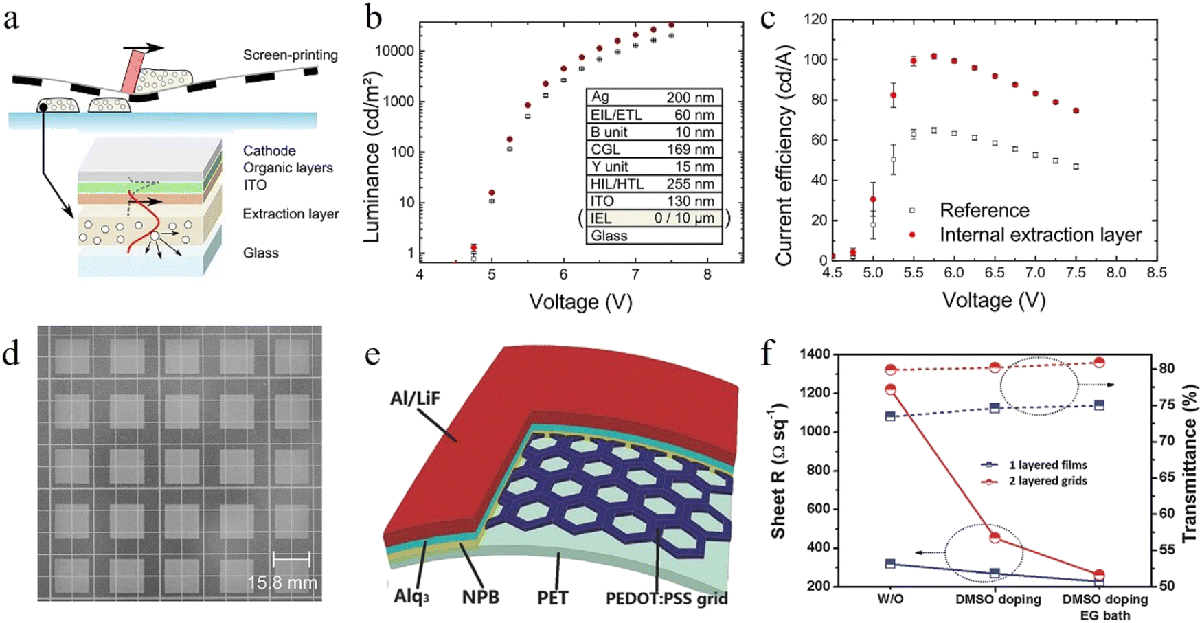 | ||
| Fig. 13 (a) Schematic diagram of the screen-printed internal extraction layer. Improved optoelectronic properties of the WOLEDs following the introduction of the IEL. (b) Luminance and (c) current efficiency of the devices with (red dots) and without (white squares) the IEL. (d) Photographic image of the complete screen-printed IEL layout.229 Copyright 2017, American Chemical Society. (e) Layer structures of experimental OLEDs with screen-printed PEDOT:PSS grid anodes. (f) Sheet resistance and light transmittance of screen-printed PEDOT:PSS anodes treated by DMSO doping and EG bath.230 Copyright 2018 Wiley-VCH Verlag GmbH & Co. KGaA, Weinheim. | ||
Compared with other similar printing methods, screen printing is not easily limited by equipment. It has the possibility of ultra-large area preparation and can be widely used in the preparation of flexible devices. However, as a mature printing technology, there are still many problems. First of all, screen printing requires a high viscosity of ink, which greatly limits the choice of materials. Therefore, it is often used in polymer printing, and there are few reports about small organic molecules with low viscosity. Secondly, although the mesh diameter can reach the micron level, the printing effect is not as good as ink-jet printing. Finally, the screen array currently used is still relatively simple, while the more complex and larger size of the screen array remains to be further studied. If the above problems can be effectively overcome, then screen printing in the field of printed electronics will have a broader application prospect.
4.4 Roll-to-roll coating
The roll-to-roll technique plays a very important role in printed electronics. It is a fabrication process of nano-scale electronic products on flexible substrates or metal films. In recent years, the preparation of large-scale flexible electronic devices has attracted much attention, and the roll-to-roll coating process is also considered as the best process for the deposition of organic electronic solution on large-scale flexible substrates.231–233Roll-to-roll coating can be divided into gravure printing, blading coating and slot-die coating. In fact, the screen printing described in the last chapter can also be regarded as a roll-to-roll coating process. However, its compatibility with roll-to-roll technology is still not ideal due to its high ink viscosity requirements and relatively slow processing speed.
000 cd m−2, which is comparable to the green OLED prepared by traditional technology at that time.192
 | ||
| Fig. 14 (a) Gravure printing process. (b) Photograph of light emission from a fully printed flexible PLED of fully gravure printed and fully spin-coated PLEDs. The size of the light emission area is 0.42 cm2 (width: 1.4 cm, height: 0.3 cm). (c) Structure of gravure printed PLEDs.192 Copyright 2010 Elsevier B.V. | ||
In terms of thickness control, the above methods can both adjust the film thickness by changing the running speed and the distance between the scraper and the substrate, but blading coating is more suitable for printing with a wide area and no fine patterns. As mentioned earlier, this kind of printing technology is highly compatible with the inks of different viscosities or different solvents, and accordingly, the requirements for the wettability of the substrate are not high. But for the water-based ink with excessive surface tension, plasma pretreatment can also be used to improve the wettability. Different from slot-die coating, double-slot-die coating can simultaneously realize the deposition of multilayer film. It can also achieve high efficiency and high yield printing with a running speed of 1 m min−1. Even though its performance is unremarkable in practical applications, it can provide a new idea for the future printed electronics.
Roll-to-roll has limitless foreground as a new kind of printing technology. First of all, from the long-term point of view, environmental protection has always been considered as the most significant point in production. Therefore, the future trend of printed electronics production needs to focus on diversification, aiming to develop different types of inks such as emulsions, solutions and nanoion dispersion solution. Besides, we can also replace the toxic solvents such as chloroform with more environmental solvents. Secondly, for roll-to-roll multilayer printing, its requirements for equipment and operation procedures are very high, which needs to be further optimized by experts in the future.
4.5 Other methods
In addition to the above printing technologies, there are also some atypical solution methods, such as the flash evaporation and dip coating.237,238 In 2017, Wang et al. reported a flash evaporation method. They first coated organic solution on a silicon substrate and then the organic solvent rapidly volatilized from the silicon wafer by changing the current of the vacuum evaporation heater.237 The organic film prepared by this method is too fast to affect the morphology of the former layer, but the development of industrial preparation will be limited by equipment. Compared with flash evaporation, the dip coating method is easier to operate and not limited by equipment. We just completely immerse the substrate in the solution for a period of time and then take it out and dry it into a film. This method is also frequently used in the experimental preparation process, which can control the thickness of the film by adjusting the soak time. Moreover, it has the advantage of high material utilization and is friendly to large-area film preparation. In 2018, Xie et al. successfully prepared the hole transport layer and small molecule luminescent layer based on the dip coating method and applied them to OLEDs. The performance of devices based on this method is even higher than that of other conventional processes.2385. Summary and perspectives
Herein, we systematically reviewed the development history, unique advantages, progress and challenges of solution-processed OLEDs for printing displays. First, we introduced the electrodes, injection layers, transport layers and emitting layers from the perspective of materials. As we all know, the widely used commercial transparent conductive films are mostly indium tin oxide (ITO). Although it can show excellent performance of more than 90% light transmittance, its high price, brittleness, poor bending resistance and other problems cannot be ignored. Therefore, it is of great significance to find a kind of transparent conductive film material which is cheap, easy to prepare, widely used and easy to integrate into flexible devices. We have studied and summarized several common conductive electrodes (metal electrodes, carbon nanomaterials, conductive polymers and composite electrodes). Then, we introduced the hole injection layers, electron injection layers, hole transport layers and electron transport layers in detail. Then, we introduced OLED printing materials from the perspective of small molecules and polymers.Second, the development, progress and difficulties of solution-processed OLEDs are introduced from the perspective of monochromicity, lamination, inversion and other structures. Compared with evaporated OLEDs, multilayer structures for solution-processed OLEDs are difficult to prepare because of the possible problems of interlayer diffusion and compatibility. In view of the above problems, this review focuses on several typical solution-processed OLED device structures and their preparation methods.
Third, we introduced various possible preparation methods of printed OLEDs, and carried out some comparative studies of the film-forming characteristics, as well as the device performance, explaining their advantages and disadvantages and development trend. Printed OLED technology includes spin-coating, inkjet-printing and screen-printing methods. In addition, the doping concentration of printed OLEDs can be accurately adjusted even though its value is very low. Here, we summarized some representative printed OLED methods and their applications in detail.
Printed OLEDs still have the following challenges: the lack of systematic basic research on the synthesis process, property regulation and engineering scaling of new materials on the electronic, atomic and molecular scales, which makes it difficult to provide theoretical guidance for the engineering scaling of material preparation; the need to consider the compatibility of the design and development with the matching ink formulation, the inkjet printing process, thin film packaging technology, etc. Printing material preparation, purification and separation are not green processes, and still face the problems of long separation and purification processes and high emission. Nevertheless, the rapid development of printed OLEDs in recent years has endowed them with great potential for their application in the future lighting and display technology. We believe that printed OLEDs prepared by inkjet printing will be the mainstream direction of the development of display technology in the future. With the improvement of printing OLED technology, the future display screens will be lighter, cheaper and clearer.
Conflicts of interest
The authors declare no conflicts of interest.Acknowledgements
The authors acknowledge the financial support from the National Key R&D Program of China (No. 2022YFE0206100), the Science and Technology Development Fund (FDCT), Macau SAR (No. 0008/2022/AMJ), the National Natural Science Foundation of China (No. 62274117 and 62075061), the Science and Technology Innovation Plan Of Shanghai Science and Technology Commission (No. 22520760600), the Jiangsu Provincial department of Science and Technology (No. BZ2022054), the Bureau of Science and Technology of Suzhou Municipality (No. SYC2022144), and the Collaborative Innovation Center of Suzhou Nano Science & Technology.References
- C. W. Tang and S. A. Vanslyke, Organic Electroluminescent Diodes, Appl. Phys. Lett., 1987, 51, 913 CrossRef CAS.
- C. Adachi, Third-generation Organic Electroluminescence Materials, Jpn. J. Appl. Phys., 2014, 53, 060101 CrossRef.
- T. Matsushima, F. Bencheikh, T. Komino, M. R. Leyden, A. S. Sandanayaka, C. Qin and C. Adachi, High performance from extraordinarily thick organic light-emitting diodes, Nature, 2019, 572, 502–506 CrossRef CAS PubMed.
- M. A. Baldo, D. F. O’Brien, Y. You, A. Shoustikov, S. Sibley, M. E. Thompson and S. R. Forrest, Highly efficient phosphorescent emission from organic electroluminescent devices, Nature, 1998, 395, 151–154 CrossRef CAS.
- Y. Sun, N. C. Giebink, H. Kanno, B. Ma, M. E. Thompson and S. R. Forrest, Management of singlet and triplet excitons for efficient white organic light-emitting devices, Nature, 2006, 440, 908–912 CrossRef CAS PubMed.
- S. Y. Byeon, D. R. Lee, K. S. Yook and J. Y. Lee, Recent progress of singlet-exciton-harvesting fluorescent organic light-emitting diodes by energy transfer processes, Adv. Mater., 2019, 31, 1803714 CrossRef PubMed.
- Y. Kondo, K. Yoshiura, S. Kitera, H. Nishi, S. Oda, H. Gotoh, Y. Sasada, M. Yanai and T. Hatakeyama, Narrowband deep-blue organic light-emitting diode featuring an organoboron-based emitter, Nat. Photonics, 2019, 13, 678–682 CrossRef CAS.
- J.-H. Lee, C.-H. Chen, P.-H. Lee, H.-Y. Lin, M.-K. Leung, T.-L. Chiu and C.-F. Lin, Blue organic light-emitting diodes: current status, challenges, and future outlook, J. Mater. Chem. C, 2019, 7, 5874–5888 RSC.
- J. H. Burroughes, D. D. Bradley, A. Brown, R. Marks, K. Mackay, R. H. Friend, P. L. Burns and A. B. Holmes, Light-emitting diodes based on conjugated polymers, Nature, 1990, 347, 539–541 CrossRef CAS.
- T. Hebner, C. Wu, D. Marcy, M. Lu and J. Sturm, Ink-jet printing of doped polymers for organic light emitting devices, Appl. Phys. Lett., 1998, 72, 519–521 CrossRef CAS.
- C. Guillen and J. Herrero, TCO/metal/TCO structures for energy and flexible electronics, Thin Solid Films, 2011, 520, 1–17 CrossRef CAS.
- D. S. Hecht, L. Hu and G. Irvin, Emerging transparent electrodes based on thin films of carbon nanotubes, graphene, and metallic nanostructures, Adv. Mater., 2011, 23, 1482–1513 CrossRef CAS PubMed.
- C. F. Guo and Z. Ren, Flexible transparent conductors based on metal nanowire networks, Mater. Today, 2015, 18, 143–154 CrossRef CAS.
- L. Hu, H. S. Kim, J.-Y. Lee, P. Peumans and Y. Cui, Scalable coating and properties of transparent, flexible, silver nanowire electrodes, ACS Nano, 2010, 4, 2955–2963 CrossRef CAS PubMed.
- J. H. Park, G. T. Hwang, S. Kim, J. Seo, H. J. Park, K. Yu, T. S. Kim and K. J. Lee, Flash-induced self-limited plasmonic welding of silver nanowire network for transparent flexible energy harvester, Adv. Mater., 2017, 29, 1603473 CrossRef PubMed.
- S. Ye, A. R. Rathmell, I. E. Stewart, Y.-C. Ha, A. R. Wilson, Z. Chen and B. J. Wiley, A rapid synthesis of high aspect ratio copper nanowires for high-performance transparent conducting films, Chem. Commun., 2014, 50, 2562–2564 RSC.
- P. E. Lyons, S. De, J. Elias, M. Schamel, L. Philippe, A. T. Bellew, J. J. Boland and J. N. Coleman, High-performance transparent conductors from networks of gold nanowires, J. Phys. Chem. Lett., 2011, 2, 3058–3062 CrossRef CAS.
- Z. Yu, L. Li, Q. Zhang, W. Hu and Q. Pei, Silver nanowire-polymer composite electrodes for efficient polymer solar cells, Adv. Mater., 2011, 23, 4453–4457 CrossRef CAS PubMed.
- D. Y. Choi, H. W. Kang, H. J. Sung and S. S. Kim, Annealing-free, flexible silver nanowire–polymer composite electrodes via a continuous two-step spray-coating method, Nanoscale, 2013, 5, 977–983 RSC.
- L. Hu, H. Wu and Y. Cui, Metal nanogrids, nanowires, and nanofibers for transparent electrodes, MRS Bull., 2011, 36, 760–765 CrossRef CAS.
- S. Hong, J. Yeo, G. Kim, D. Kim, H. Lee, J. Kwon, H. Lee, P. Lee and S. H. Ko, Nonvacuum, maskless fabrication of a flexible metal grid transparent conductor by low-temperature selective laser sintering of nanoparticle ink, ACS Nano, 2013, 7, 5024–5031 CrossRef CAS PubMed.
- J. Schneider, P. Rohner, D. Thureja, M. Schmid, P. Galliker and D. Poulikakos, Electrohydrodynamic nanodrip printing of high aspect ratio metal grid transparent electrodes, Adv. Funct. Mater., 2016, 26, 833–840 CrossRef CAS.
- J. W. Lim, Y. T. Lee, R. Pandey, T.-H. Yoo, B.-I. Sang, B.-K. Ju, D. K. Hwang and W. K. Choi, Effect of geometric lattice design on optical/electrical properties of transparent silver grid for organic solar cells, Opt. Express, 2014, 22, 26891–26899 CrossRef CAS PubMed.
- J. H. Maurer, L. González-García, B. Reiser, I. Kanelidis and T. Kraus, Templated self-assembly of ultrathin gold nanowires by nanoimprinting for transparent flexible electronics, Nano Lett., 2016, 16, 2921–2925 CrossRef CAS PubMed.
- H. Wu, D. Kong, Z. Ruan, P.-C. Hsu, S. Wang, Z. Yu, T. J. Carney, L. Hu, S. Fan and Y. Cui, A transparent electrode based on a metal nanotrough network, Nat. Nanotechnol., 2013, 8, 421–425 CrossRef CAS PubMed.
- M. G. Kang and L. J. Guo, Nanoimprinted semitransparent metal electrodes and their application in organic light-emitting diodes, Adv. Mater., 2007, 19, 1391–1396 CrossRef CAS.
- X. Chen, W. Guo, L. Xie, C. Wei, J. Zhuang, W. Su and Z. Cui, Embedded Ag/Ni metal-mesh with low surface roughness as transparent conductive electrode for optoelectronic applications, ACS Appl. Mater. Interfaces, 2017, 9, 37048–37054 CrossRef CAS PubMed.
- C. Zhang, D. Zhao, D. Gu, H. Kim, T. Ling, Y. K. R. Wu and L. J. Guo, An ultrathin, smooth, and low-loss Al-doped Ag film and its application as a transparent electrode in organic photovoltaics, Adv. Mater., 2014, 26, 5696–5701 CrossRef CAS PubMed.
- S. Schubert, J. Meiss, L. Müller-Meskamp and K. Leo, Improvement of transparent metal top electrodes for organic solar cells by introducing a high surface energy seed layer, Adv. Energy Mater., 2013, 3, 438–443 CrossRef CAS.
- S. Schubert, M. Hermenau, J. Meiss, L. Müller-Meskamp and K. Leo, Oxide sandwiched metal thin-film electrodes for long-term stable organic solar cells, Adv. Funct. Mater., 2012, 22, 4993–4999 CrossRef CAS.
- H. M. Stec, R. J. Williams, T. S. Jones and R. A. Hatton, Ultrathin Transparent Au Electrodes for Organic Photovoltaics Fabricated Using a Mixed Mono-Molecular Nucleation Layer, Adv. Funct. Mater., 2011, 21, 1709–1716 CrossRef CAS.
- J. Zou, C. Z. Li, C. Y. Chang, H. L. Yip and A. K. Y. Jen, Interfacial engineering of ultrathin metal film transparent electrode for flexible organic photovoltaic cells, Adv. Mater., 2014, 26, 3618–3623 CrossRef CAS PubMed.
- H. Kang, S. Jung, S. Jeong, G. Kim and K. Lee, Polymer-metal hybrid transparent electrodes for flexible electronics, Nat. Commun., 2015, 6, 1–7 Search PubMed.
- R. R. Nair, P. Blake, A. N. Grigorenko, K. S. Novoselov, T. J. Booth, T. Stauber, N. M. Peres and A. K. Geim, Fine structure constant defines visual transparency of graphene, Science, 2008, 320, 1308 CrossRef CAS PubMed.
- Z. Zhang, J. Du, D. Zhang, H. Sun, L. Yin, L. Ma, J. Chen, D. Ma, H.-M. Cheng and W. Ren, Rosin-enabled ultraclean and damage-free transfer of graphene for large-area flexible organic light-emitting diodes, Nat. Commun., 2017, 8, 1–9 CrossRef PubMed.
- J. S. Bunch, S. S. Verbridge, J. S. Alden, A. M. Van Der Zande, J. M. Parpia, H. G. Craighead and P. L. McEuen, Impermeable atomic membranes from graphene sheets, Nano Lett., 2008, 8, 2458–2462 CrossRef CAS PubMed.
- H.-K. Seo, M.-H. Park, Y.-H. Kim, S.-J. Kwon, S.-H. Jeong and T.-W. Lee, Laminated graphene films for flexible transparent thin film encapsulation, ACS Appl. Mater. Interfaces, 2016, 8, 14725–14731 CrossRef PubMed.
- K. S. Novoselov, L. Colombo, P. Gellert, M. Schwab and K. Kim, A roadmap for graphene, Nature, 2012, 490, 192–200 CrossRef CAS PubMed.
- H. Kim, S.-H. Bae, T.-H. Han, K.-G. Lim, J.-H. Ahn and T.-W. Lee, Organic solar cells using CVD-grown graphene electrodes, Nanotechnology, 2013, 25, 014012 CrossRef PubMed.
- H. Park, Y. M. Shi and J. Kong, Application of solvent modified PEDOT:PSS to graphene electrodes in organic solar cells, Nanoscale, 2013, 5, 8934–8939 RSC.
- Y. Zhou, C. Fuentes-Hernandez, J. Shim, J. Meyer, A. J. Giordano, H. Li, P. Winget, T. Papadopoulos, H. Cheun and J. Kim, A universal method to produce low–work function electrodes for organic electronics, Science, 2012, 336, 327–332 CrossRef CAS PubMed.
- J.-K. Chang, W.-H. Lin, J.-I. Taur, T.-H. Chen, G.-K. Liao, T.-W. Pi, M.-H. Chen and C.-I. Wu, Graphene anodes and cathodes: tuning the work function of graphene by nearly 2 eV with an aqueous intercalation process, ACS Appl. Mater. Interfaces, 2015, 7, 17155–17161 CrossRef CAS PubMed.
- S. Iijima and T. Ichihashi, Single-shell carbon nanotubes of 1-nm diameter, Nature, 1993, 363, 603–605 CrossRef CAS.
- Z. Wu, Z. Chen, X. Du, J. M. Logan, J. Sippel, M. Nikolou, K. Kamaras, J. R. Reynolds, D. B. Tanner and A. F. Hebard, Transparent, conductive carbon nanotube films, Science, 2004, 305, 1273–1276 CrossRef CAS PubMed.
- E. Snow, J. Novak, P. Campbell and D. Park, Random networks of carbon nanotubes as an electronic material, Appl. Phys. Lett., 2003, 82, 2145–2147 CrossRef CAS.
- J. Du, S. Pei, L. Ma and H. M. Cheng, 25th anniversary article: carbon nanotube-and graphene-based transparent conductive films for optoelectronic devices, Adv. Mater., 2014, 26, 1958–1991 CrossRef CAS PubMed.
- A. Perumal, H. Faber, N. Yaacobi-Gross, P. Pattanasattayavong, C. Burgess, S. Jha, M. A. McLachlan, P. N. Stavrinou, T. D. Anthopoulos and D. D. Bradley, High-efficiency, solution-processed, multilayer phosphorescent organic light-emitting diodes with a copper thiocyanate hole-injection/hole-transport layer, Adv. Mater., 2015, 27, 93–100 CrossRef CAS PubMed.
- J. Kim, J. Jung, D. Lee and J. Joo, Enhancement of electrical conductivity of poly(3,4-ethylenedioxythiophene)/poly(4-styrenesulfonate) by a change of solvents, Synth. Met., 2002, 126, 311–316 CrossRef CAS.
- C. Badre, L. Marquant, A. M. Alsayed and L. A. Hough, Highly Conductive Poly(3,4-ethylenedioxythiophene):Poly(styrenesulfonate) Films Using 1-Ethyl-3-methylimidazolium Tetracyanoborate Ionic Liquid, Adv. Funct. Mater., 2002, 2723–2727 Search PubMed.
- W. Zhang, B. Zhao, Z. He, X. Zhao, H. Wang, S. Yang, H. Wu and Y. Cao, High-efficiency ITO-free polymer solar cells using highly conductive PEDOT:PSS/surfactant bilayer transparent anodes, Energy Environ. Sci., 2013, 1956–1964 RSC.
- D. A. Mengistie, M. A. Ibrahem, P. C. Wang and C. W. Chu, Highly conductive PEDOT:PSS treated with formic acid for ITO-free polymer solar cells, ACS Appl. Mater. Interfaces, 2014, 6, 2292–2299 CrossRef CAS PubMed.
- M. Wei, G. Ru, Z. Li, J. Tong and Y. Zhou, Conductivity Enhancement of PEDOT:PSS Films via Phosphoric Acid Treatment for Flexible All-Plastic Solar Cells, ACS Appl. Mater. Interfaces, 2015, 7, 14089–140094 CrossRef PubMed.
- N. Kim, S. Kee, S. H. Lee, B. H. Lee, Y. H. Kahng, Y. R. Jo, B. J. Kim and K. Lee, Highly conductive PEDOT: PSS nanofibrils induced by solution-processed crystallization, Adv. Mater., 2014, 26, 2268–2272 CrossRef CAS PubMed.
- I. N. Kholmanov, S. H. Domingues, H. Chou, X. Wang, C. Tan, J.-Y. Kim, H. Li, R. Piner, A. J. Zarbin and R. S. Ruoff, Reduced graphene oxide/copper nanowire hybrid films as high-performance transparent electrodes, ACS Nano, 2013, 7, 1811–1816 CrossRef CAS PubMed.
- I. N. Kholmanov, C. W. Magnuson, A. E. Aliev, H. Li, B. Zhang, J. W. Suk, L. L. Zhang, E. Peng, S. H. Mousavi and A. B. Khanikaev, Improved electrical conductivity of graphene films integrated with metal nanowires, Nano Lett., 2012, 12, 5679–5683 CrossRef CAS PubMed.
- H. Chang, G. Wang, A. Yang, X. Tao, X. Liu, Y. Shen and Z. Zheng, A transparent, flexible, low-temperature, and solution-processible graphene composite electrode, Adv. Funct. Mater., 2010, 20, 2893–2902 CrossRef CAS.
- M. Helander, Z. Wang, J. Qiu, M. Greiner, D. Puzzo, Z. Liu and Z. Lu, Chlorinated indium tin oxide electrodes with high work function for organic device compatibility, Science, 2011, 332, 944–947 CrossRef CAS PubMed.
- H. Ishii, K. Sugiyama, E. Ito and K. Seki, Energy level alignment and interfacial electronic structures at organic/metal and organic/organic interfaces, Adv. Mater., 1999, 11, 605–625 CrossRef CAS.
- H.-W. Lin, W.-C. Lin, J.-H. Chang and C.-I. Wu, Solution-processed hexaazatriphenylene hexacarbonitrile as a universal hole-injection layer for organic light-emitting diodes, Org. Electron., 2013, 14, 1204–1210 CrossRef CAS.
- S. Ho, C. Xiang, R. Liu, N. Chopra, M. Mathai and F. So, Stable solution processed hole injection material for organic light-emitting diodes, Org. Electron., 2014, 15, 2513–2517 CrossRef CAS.
- Y. Chen, Y. Xia, G. M. Smith, H. Sun, D. Yang, D. Ma, Y. Li, W. Huang and D. L. Carroll, Solution-processable hole-generation layer and electron-transporting layer: towards high-performance, alternating-current-driven, field-induced polymer electroluminescent devices, Adv. Funct. Mater., 2014, 24, 2677–2688 CrossRef CAS.
- A. Elschner, F. Bruder, H.-W. Heuer, F. Jonas, A. Karbach, S. Kirchmeyer, S. Thurm and R. Wehrmann, PEDT/PSS for efficient hole-injection in hybrid organic light-emitting diodes, Synth. Met., 2000, 111, 139–143 CrossRef.
- T. M. Brown, J.-S. Kim, R. H. Friend, F. Cacialli, R. Daik and W. J. Feast, Built-in field electroabsorption spectroscopy of polymer light-emitting diodes incorporating a doped poly(3, 4-ethylene dioxythiophene) hole injection layer, Appl. Phys. Lett., 1999, 75, 1679–1681 CrossRef CAS.
- E. Voroshazi, B. Verreet, A. Buri, R. Müller, D. Di Nuzzo and P. Heremans, Influence of cathode oxidation via the hole extraction layer in polymer: fullerene solar cells, Org. Electron., 2011, 12, 736–744 CrossRef CAS.
- M. Jørgensen, K. Norrman and F. C. Krebs, Stability/degradation of polymer solar cells, Sol. Energy Mater. Sol. Cells, 2008, 92, 686–714 CrossRef.
- S. Nau, N. Schulte, S. Winkler, J. Frisch, A. Vollmer, N. Koch, S. Sax and E. J. List, Highly Efficient Color-Stable Deep-Blue Multilayer PLEDs: Preventing PEDOT: PSS-Induced Interface Degradation, Adv. Mater., 2013, 25, 4420–4424 CrossRef CAS PubMed.
- J.-S. Kim, R. H. Friend, I. Grizzi and J. H. Burroughes, Spin-cast thin semiconducting polymer interlayer for improving device efficiency of polymer light-emitting diodes, Appl. Phys. Lett., 2005, 87, 023506 CrossRef.
- T. W. Lee, Y. Chung, O. Kwon and J. J. Park, Self-organized gradient hole injection to improve the performance of polymer electroluminescent devices, Adv. Funct. Mater., 2007, 17, 390–396 CrossRef CAS.
- T. Chiba, Y. J. Pu and J. Kido, Solution-processed white phosphorescent tandem organic light-emitting devices, Adv. Mater., 2015, 27, 4681–4687 CrossRef CAS PubMed.
- M. Zhang, S. Höfle, J. Czolk, A. Mertens and A. Colsmann, All-solution processed transparent organic light emitting diodes, Nanoscale, 2015, 7, 20009–20014 RSC.
- A. De Girolamo Del Mauro, G. Nenna, V. Bizzarro, I. A. Grimaldi, F. Villani and C. Minarini, Analysis of the performances of organic light-emitting devices with a doped or an undoped polyaniline–poly(4-styrenesulfonate) hole-injection layer, J. Appl. Polym. Sci., 2011, 122, 3618–3623 CrossRef CAS.
- K. R. Choudhury, J. Lee, N. Chopra, A. Gupta, X. Jiang, F. Amy and F. So, Highly efficient hole injection using polymeric anode materials for small-molecule organic light-emitting diodes, Adv. Funct. Mater., 2009, 19, 491–496 CrossRef CAS.
- D. Dong, J. Xia, S. Yang, X. Wu, B. Wei, L. Lian, D. Feng, Y. Zheng and G. He, Hole-transporting small molecules as a mixed host for efficient solution processed green phosphorescent organic light emitting diodes, Org. Electron., 2016, 38, 29–34 CrossRef CAS.
- J. Liu, X. Wu, S. Chen, X. Shi, J. Wang, S. Huang, X. Guo and G. He, Low-temperature MoO 3 film from a facile synthetic route for an efficient anode interfacial layer in organic optoelectronic devices, J. Mater. Chem. C, 2014, 2, 158–163 RSC.
- Q. Fu, J. Chen, C. Shi and D. Ma, Room-temperature sol–gel derived molybdenum oxide thin films for efficient and stable solution-processed organic light-emitting diodes, ACS Appl. Mater. Interfaces, 2013, 5, 6024–6029 CrossRef CAS PubMed.
- I. Hancox, L. Rochford, D. Clare, M. Walker, J. Mudd, P. Sullivan, S. Schumann, C. McConville and T. Jones, Optimization of a high work function solution processed vanadium oxide hole-extracting layer for small molecule and polymer organic photovoltaic cells, J. Phys. Chem. C, 2013, 117, 49–57 CrossRef CAS.
- S. Liu, R. Liu, Y. Chen, S. Ho, J. H. Kim and F. So, Nickel oxide hole injection/transport layers for efficient solution-processed organic light-emitting diodes, Chem. Mater., 2014, 26, 4528–4534 CrossRef CAS.
- S. Höfle, M. Bruns, S. Strässle, C. Feldmann, U. Lemmer and A. Colsmann, Tungsten Oxide Buffer Layers Fabricated in an Inert Sol-Gel Process at Room-Temperature for Blue Organic Light-Emitting Diodes, Adv. Mater., 2013, 25, 4113–4116 CrossRef PubMed.
- K. Zilberberg, S. Trost, H. Schmidt and T. Riedl, Solution processed vanadium pentoxide as charge extraction layer for organic solar cells, Adv. Energy Mater., 2011, 1, 377–381 CrossRef CAS.
- K. Zilberberg, S. Trost, J. Meyer, A. Kahn, A. Behrendt, D. Lützenkirchen-Hecht, R. Frahm and T. Riedl, Inverted organic solar cells with sol–gel processed high work-function vanadium oxide hole-extraction layers, Adv. Funct. Mater., 2011, 21, 4776–4783 CrossRef CAS.
- J. Meyer, S. Hamwi, M. Kröger, W. Kowalsky, T. Riedl and A. Kahn, Transition metal oxides for organic electronics: energetics, device physics and applications, Adv. Mater., 2012, 24, 5408–5427 CrossRef CAS PubMed.
- S. Murase and Y. Yang, Solution processed MoO3 interfacial layer for organic photovoltaics prepared by a facile synthesis method, Adv. Mater., 2012, 24, 2459–2462 CrossRef CAS PubMed.
- C. Girotto, E. Voroshazi, D. Cheyns, P. Heremans and B. P. Rand, Solution-processed MoO3 thin films as a hole-injection layer for organic solar cells, ACS Appl. Mater. Interfaces, 2011, 3, 3244–3247 CrossRef CAS PubMed.
- I. Irfan, A. James Turinske, Z. Bao and Y. Gao, Work function recovery of air exposed molybdenum oxide thin films, Appl. Phys. Lett., 2012, 101, 093305 CrossRef.
- S. R. Hammond, J. Meyer, N. E. Widjonarko, P. F. Ndione, A. K. Sigdel, A. Garcia, A. Miedaner, M. T. Lloyd, A. Kahn and D. S. Ginley, Low-temperature, solution-processed molybdenum oxide hole-collection layer for organic photovoltaics, J. Mater. Chem., 2012, 22, 3249–3254 RSC.
- N. Wijeyasinghe, A. Regoutz, F. Eisner, T. Du, L. Tsetseris, Y. H. Lin, H. Faber, P. Pattanasattayavong, J. Li and F. Yan, Copper (I) thiocyanate (CuSCN) hole-transport layers processed from aqueous precursor solutions and their application in thin-film transistors and highly efficient organic and organometal halide perovskite solar cells, Adv. Funct. Mater., 2017, 27, 1701818 CrossRef.
- N. Yaacobi-Gross, N. D. Treat, P. Pattanasattayavong, H. Faber, A. K. Perumal, N. Stingelin, D. D. Bradley, P. N. Stavrinou, M. Heeney and T. D. Anthopoulos, High-Efficiency Organic Photovoltaic Cells Based on the Solution-Processable Hole Transporting Interlayer Copper Thiocyanate (CuSCN) as a Replacement for PEDOT: PSS, Adv. Energy Mater., 2015, 5, 1401529 CrossRef.
- A. Heeger, Conducting polymers for carbon electronics themed issue, Chem. Soc. Rev., 2010, 39, 2351 RSC.
- F. Huang, L. Hou, H. Wu, X. Wang, H. Shen, W. Cao, W. Yang and Y. Cao, High-efficiency, environment-friendly electroluminescent polymers with stable high work function metal as a cathode: Green-and yellow-emitting conjugated polyfluorene polyelectrolytes and their neutral precursors, J. Am. Chem. Soc., 2004, 126, 9845–9853 CrossRef CAS PubMed.
- H. Wu, F. Huang, J. Peng and Y. Cao, High-efficiency electron injection cathode of Au for polymer light-emitting devices, Org. Electron., 2005, 6, 118–128 CrossRef CAS.
- K. Zhang, C. Zhong, S. Liu, A.-h Liang, S. Dong and F. Huang, High efficiency solution processed inverted white organic light emitting diodes with a cross-linkable amino-functionalized polyfluorene as a cathode interlayer, J. Mater. Chem. C, 2014, 2, 3270–3277 RSC.
- C. Zhong, S. Liu, F. Huang, H. Wu and Y. Cao, Highly efficient electron injection from indium tin oxide/cross-linkable amino-functionalized polyfluorene interface in inverted organic light emitting devices, Chem. Mater., 2011, 23, 4870–4876 CrossRef CAS.
- S. Liu, C. Zhong, J. Zhang, C. Duan, X. Wang and F. Huang, A novel crosslinkable electron injection/transporting material for solution processed polymer light-emitting diodes, Sci. China: Chem., 2011, 54, 1745–1749 CrossRef CAS.
- J. Wang, K. Lin, K. Zhang, X. F. Jiang, K. Mahmood, L. Ying, F. Huang and Y. Cao, Crosslinkable Amino-Functionalized Conjugated Polymer as Cathode Interlayer for Efficient Inverted Polymer Solar Cells, Adv. Energy Mater., 2016, 6, 1502563 CrossRef.
- D. Li, C. Sun, H. Li, H. Shi, X. Shai, Q. Sun, J. Han, Y. Shen, H.-L. Yip and F. Huang, Amino-functionalized conjugated polymer electron transport layers enhance the UV-photostability of planar heterojunction perovskite solar cells, Chem. Sci., 2017, 8, 4587–4594 RSC.
- C. Sun, Z. Wu, Z. Hu, J. Xiao, W. Zhao, H.-W. Li, Q.-Y. Li, S.-W. Tsang, Y.-X. Xu and K. Zhang, Interface design for high-efficiency non-fullerene polymer solar cells, Energy Environ. Sci., 2017, 10, 1784–1791 RSC.
- S. L. Kwak, H. J. Park, J.-H. Jang, J. Y. Park, J. M. Park, J. Lee and D.-H. Hwang, Synthesis and characterization of thermally cross-linkable poly(iminoarylene)-based hole injection layer for solution-processed organic light-emitting diodes, Chem. Eng. J., 2023, 454, 139944 CrossRef.
- F. Huang, P. I. Shih, C. F. Shu, Y. Chi and A. K. Y. Jen, Highly efficient polymer white-light-emitting diodes based on lithium salts doped electron transporting layer, Adv. Mater., 2009, 21, 361–365 CrossRef CAS.
- P. Jing, W. Ji, Q. Zeng, D. Li, S. Qu, J. Wang and D. Zhang, Vacuum-free transparent quantum dot light-emitting diodes with silver nanowire cathode, Sci. Rep., 2015, 5, 1–8 Search PubMed.
- F. Guo, H. Azimi, Y. Hou, T. Przybilla, M. Hu, C. Bronnbauer, S. Langner, E. Spiecker, K. Forberich and C. J. Brabec, High-performance semitransparent perovskite solar cells with solution-processed silver nanowires as top electrodes, Nanoscale, 2015, 7, 1642–1649 RSC.
- C. Song, Z. Hu, Y. Luo, Y. Cun, L. Wang, L. Ying, F. Huang, J. Peng, J. Wang and Y. Cao, Organic/Inorganic Hybrid EIL for All-Solution-Processed OLEDs, Adv. Electron. Mater., 2018, 4, 1700380 CrossRef.
- G. Wetzelaer, A. Najafi, R. Kist, M. Kuik and P. W. Blom, Efficient electron injection from solution-processed cesium stearate interlayers in organic light-emitting diodes, Appl. Phys. Lett., 2013, 102, 22 CrossRef.
- J. Huang, G. Li, E. Wu, Q. Xu and Y. Yang, Achieving high-efficiency polymer white-light-emitting devices, Adv. Mater., 2006, 18, 114–117 CrossRef CAS.
- J. Huang, Z. Xu and Y. Yang, Low-work-function surface formed by solution-processed and thermally deposited nanoscale layers of cesium carbonate, Adv. Funct. Mater., 2007, 17, 1966–1973 CrossRef CAS.
- J. J. Park, T. J. Park, W. S. Jeon, R. Pode, J. Jang, J. H. Kwon, E.-S. Yu and M.-Y. Chae, Small molecule interlayer for solution processed phosphorescent organic light emitting device, Org. Electron., 2009, 10, 189–193 CrossRef CAS.
- D.-H. Kim, D. H. Choi, J. J. Park, S. T. Lee and J. H. Kwon, Novel green small-molecule host materials for solution-processed organic light-emitting diodes, Chem. Lett., 2008, 37, 1150–1151 CrossRef CAS.
- S. A. Van Slyke, C. Chen and C. W. Tang, Organic electroluminescent devices with improved stability, Appl. Phys. Lett., 1996, 69, 2160–2162 CrossRef CAS.
- C. Adachi, T. Tsutsui and S. Saito, Organic electroluminescent device having a hole conductor as an emitting layer, Appl. Phys. Lett., 1989, 55, 1489–1491 CrossRef CAS.
- L. B. Schein, Comparison of charge transport models in molecularly doped polymers, Philos. Mag. B, 1992, 65, 795–810 CAS.
- J. Salbeck, N. Yu, J. Bauer, F. Weissörtel and H. Bestgen, Low molecular organic glasses for blue electroluminescence, Synth. Met., 1997, 91, 209–215 CrossRef CAS.
- Y. Shirota, Y. Kuwabara, H. Inada, T. Wakimoto, H. Nakada, Y. Yonemoto, S. Kawami and K. Imai, Multilayered organic electroluminescent device using a novel starburst molecule, 4, 4′, 4′-tris (3-methylphenylphenylamino) triphenylamine, as a hole transport material, Appl. Phys. Lett., 1994, 65, 807–809 CrossRef CAS.
- Y. Shirota, Photo-and electroactive amorphous molecular materials—molecular design, syntheses, reactions, properties, and applications, J. Mater. Chem., 2005, 15, 75–93 RSC.
- A. Mishra, P. Nayak, D. Ray, M. Patankar, K. Narasimhan and N. Periasamy, Synthesis and characterization of spin-coatable tert-amine molecules for hole-transport in organic light-emitting diodes, Tetrahedron Lett., 2006, 47, 4715–4719 CrossRef CAS.
- T. Ito, J. Asaka, K. L. T. Dao and J. Kido, Organic light-emitting devices having chemically-doped arylamine oligomer as a hole injection layer, Polym. Adv. Technol., 2005, 16, 559–562 CrossRef CAS.
- M. Nomuraa, Y. Shibasakia, M. Ueda, K. Tugitab, M. Ichikawab and Y. Taniguchib, Synthesis of thermally stable and hole-transporting amorphous molecule having four carbazole moieties, Synth. Met., 2005, 148, 155–160 CrossRef.
- H. Ha, Y. J. Shim, D. H. Lee, E. Y. Park, I.-H. Lee, S.-K. Yoon and M. C. Suh, Highly efficient solution-processed organic light-emitting diodes containing a new cross-linkable hole transport material blended with commercial hole transport materials, ACS Appl. Mater. Interfaces, 2021, 13, 21954–21963 CrossRef CAS PubMed.
- C. Peng, H. Liu, X. Han, F. Zhang, S. Wang and X. Li, Construction of a fully conjugated cross-linked hole-transport film based on ethynyl to enable high mobility for efficient solution-processed OLEDs, J. Mater. Chem. C, 2022, 10, 14471–14479 RSC.
- H. R. Tseng, H. F. Meng, K. C. Lee and S. F. Horng, Multilayer Polymer Light-Emitting Diodes by Blade Coating Method, Dig. Tech. Pap. - Soc. Inf. Disp. Int. Symp., 2008, 39, 2067–2070 CrossRef CAS.
- M. Nomura, Y. Shibasaki, M. Ueda, K. Tugita, M. Ichikawa and Y. Taniguchi, New amorphous electron-transporting materials based on Tris-benzimidazoles for all wet-process OLED devices, Synth. Met., 2005, 151, 261–268 CrossRef CAS.
- S. J. Su, Y. Takahashi, T. Chiba, T. Takeda and J. Kido, Structure–Property Relationship of Pyridine-Containing Triphenyl Benzene Electron-Transport Materials for Highly Efficient Blue Phosphorescent OLEDs, Adv. Funct. Mater., 2009, 19, 1260–1267 CrossRef CAS.
- S. J. Su, T. Chiba, T. Takeda and J. Kido, Pyridine-containing triphenylbenzene derivatives with high electron mobility for highly efficient phosphorescent OLEDs, Adv. Mater., 2008, 20, 2125–2130 CrossRef CAS.
- R. H. Friend, R. Gymer, A. Holmes, J. Burroughes, R. Marks, C. Taliani, D. Bradley, D. Dos Santos, J.-L. Bredas and M. Lögdlund, Electroluminescence in conjugated polymers, Nature, 1999, 397, 121–128 CrossRef CAS.
- L. J. Rothberg and A. J. Lovinger, Status of and prospects for organic electroluminescence, J. Mater. Res., 1996, 11, 3174–3187 CrossRef CAS.
- A. Brown, D. Bradley, J. Burroughes, R. Friend, N. Greenham, P. Burn, A. Holmes and A. Kraft, Poly(p-phenylenevinylene) light-emitting diodes: Enhanced electroluminescent efficiency through charge carrier confinement, Appl. Phys. Lett., 1992, 61, 2793–2795 CrossRef CAS.
- L. Swanson, J. Shinar, A. Brown, D. C. Bradley, R. Friend, P. Burn, A. Kraft and A. Holmes, Electroluminescence-detected magnetic-resonance study of polyparaphenylenevinylene (PPV)-based light-emitting diodes, Phys. Rev. B: Condens. Matter Mater. Phys., 1992, 46, 15072 CrossRef CAS PubMed.
- C. Adachi, M. A. Baldo, M. E. Thompson and S. R. Forrest, Nearly 100% internal phosphorescence efficiency in an organic light-emitting device, J. Appl. Phys., 2001, 90, 5048–5051 CrossRef CAS.
- M. Kim and J. Y. Lee, Engineering the substitution position of diphenylphosphine oxide at carbazole for thermal stability and high external quantum efficiency above 30% in blue phosphorescent organic light-emitting diodes, Adv. Funct. Mater., 2014, 24, 4164–4169 CrossRef CAS.
- S. J. Su, H. Sasabe, Y. J. Pu, K. i Nakayama and J. Kido, Tuning Energy Levels of Electron-Transport Materials by Nitrogen Orientation for Electrophosphorescent Devices with an ‘Ideal’Operating Voltage, Adv. Mater., 2010, 22, 3311–3316 CrossRef CAS PubMed.
- K. Udagawa, H. Sasabe, C. Cai and J. Kido, Low-driving-voltage blue phosphorescent organic light-emitting devices with external quantum efficiency of 30%, Adv. Mater., 2014, 26, 5062–5066 CrossRef CAS PubMed.
- X. Xing, T. Lin, Y.-X. Hu, Y.-L. Sun, W.-Y. Mu, Z.-Z. Du, Y.-K. Liu, D.-F. Yang, S.-L. Shi and D.-Y. Zhang, Inkjet printing high luminance phosphorescent OLED based on m-MTDATA: TPBi host, Mod. Phys. Lett. B, 2019, 33, 1950149 CrossRef CAS.
- L. Mu, M. He, C. Jiang, J. Wang, C. Mai, X. Huang, H. Zheng, J. Wang, X.-H. Zhu and J. Peng, Inkjet printing a small-molecule binary emitting layer for organic light-emitting diodes, J. Mater. Chem. C, 2020, 8, 6906–6913 RSC.
- J. Zhang, Y. Guan, J. Yang, W. Hua, S. Wang, Z. Ling, H. Lian, Y. Liao, W. Lan and B. Wei, Highly-efficient solution-processed green phosphorescent organic light-emitting diodes with reduced efficiency roll-off using ternary blend hosts, J. Mater. Chem. C, 2019, 7, 11109–11117 RSC.
- H. Uoyama, K. Goushi, K. Shizu, H. Nomura and C. Adachi, Highly efficient organic light-emitting diodes from delayed fluorescence, Nature, 2012, 492, 234–238 CrossRef CAS PubMed.
- S. Y. Lee, T. Yasuda, Y. S. Yang, Q. Zhang and C. Adachi, Luminous butterflies: efficient exciton harvesting by benzophenone derivatives for full-color delayed fluorescence OLEDs, Angew. Chem., Int. Ed., 2014, 53, 6402–6406 CrossRef CAS PubMed.
- S. K. Jeon, H. L. Lee, K. S. Yook and J. Y. Lee, Recent progress of the lifetime of organic light-emitting diodes based on thermally activated delayed fluorescent material, Adv. Mater., 2019, 31, 1803524 CrossRef PubMed.
- Y. Shu and B. G. Levine, Simulated evolution of fluorophores for light emitting diodes, J. Chem. Phys., 2015, 142, 104104 CrossRef PubMed.
- D. H. Ahn, S. W. Kim, H. Lee, I. J. Ko, D. Karthik, J. Y. Lee and J. H. Kwon, Highly efficient blue thermally activated delayed fluorescence emitters based on symmetrical and rigid oxygen-bridged boron acceptors, Nat. Photonics, 2019, 13, 540–546 CrossRef CAS.
- A. Verma, D. M. Zink, C. Fléchon, J. Leganés Carballo, H. Flügge, J. M. Navarro, T. Baumann and D. Volz, Efficient, inkjet-printed TADF-OLEDs with an ultra-soluble NHetPHOS complex, Appl. Phys. A, 2016, 122, 1–5 CrossRef CAS.
- C. Amruth, B. Luszczynska, M. Z. Szymanski, J. Ulanski, K. Albrecht and K. Yamamoto, Inkjet printing of thermally activated delayed fluorescence (TADF) dendrimer for OLEDs applications, Org. Electron., 2019, 74, 218–227 CrossRef.
- L. Hu, J. Liang, W. Zhong, T. Guo, Z. Zhong, F. Peng, B. Fan, L. Ying and Y. Cao, Improving the electroluminescence performance of blue light-emitting poly(fluorene-co-dibenzothiophene-S,S-dioxide) by tuning the intra-molecular charge transfer effects and temperature-induced orientation of the emissive layer structure, J. Mater. Chem. C, 2019, 7, 5630–5638 RSC.
- S. Shao, J. Hu, X. Wang, L. Wang, X. Jing and F. Wang, Blue thermally activated delayed fluorescence polymers with nonconjugated backbone and through-space charge transfer effect, J. Am. Chem. Soc., 2017, 139, 17739–17742 CrossRef CAS PubMed.
- J. A. McEwan, A. J. Clulow, A. Nelson, R. D. Jansen-van Vuuren, P. L. Burn and I. R. Gentle, Morphology of OLED Film Stacks Containing Solution-Processed Phosphorescent Dendrimers, ACS Appl. Mater. Interfaces, 2018, 10, 3848–3855 CrossRef CAS PubMed.
- S. Scholz, D. Kondakov, B. Lussem and K. Leo, Degradation mechanisms and reactions in organic light-emitting devices, Chem. Rev., 2015, 115, 8449–8503 CrossRef CAS PubMed.
- C. D. Müller, A. Falcou, N. Reckefuss, M. Rojahn, V. Wiederhirn, P. Rudati, H. Frohne, O. Nuyken, H. Becker and K. Meerholz, Multi-colour organic light-emitting displays by solution processing, Nature, 2003, 421, 829–833 CrossRef PubMed.
- K. Meerholz, Enlightening solutions, Nature, 2005, 437, 327–328 CrossRef CAS PubMed.
- S. Wang, B. Zhang, Y. Wang, J. Ding, Z. Xie and L. Wang, Solution-processed multilayer green electrophosphorescent devices with self-host iridium dendrimers as the nondoped emitting layer: achieving high efficiency while avoiding redissolution-induced batch-to-batch variation, Chem. Commun., 2017, 53, 5128–5131 RSC.
- K. W. Tsai, M. K. Hung, Y. H. Mao and S. A. Chen, Solution-processed thermally activated delayed fluorescent OLED with high EQE as 31% using high triplet energy crosslinkable hole transport materials, Adv. Funct. Mater., 2019, 29, 1901025 CrossRef.
- K. S. Yook and J. Y. Lee, Small molecule host materials for solution processed phosphorescent organic light-emitting diodes, Adv. Mater., 2014, 26, 4218–4233 CrossRef CAS PubMed.
- G. Tu, C. Mei, Q. Zhou, Y. Cheng, Y. Geng, L. Wang, D. Ma, X. Jing and F. Wang, Highly Efficient Pure-White-Light-Emitting Diodes from a Single Polymer: Polyfluorene with Naphthalimide Moieties, Adv. Funct. Mater., 2006, 16, 101–106 CrossRef CAS.
- H. Wu, J. Zou, F. Liu, L. Wang, A. Mikhailovsky, G. C. Bazan, W. Yang and Y. Cao, Efficient single active layer electrophosphorescent white polymer light-emitting diodes, Adv. Mater., 2008, 20, 696–702 CrossRef CAS.
- J. Kido, H. Shionoya and K. Nagai, Single-layer white light-emitting organic electroluminescent devices based on dye-dispersed poly(N-vinylcarbazole), Appl. Phys. Lett., 1995, 67, 2281–2283 CrossRef CAS.
- K. T. Kamtekar, A. P. Monkman and M. R. Bryce, Recent advances in white organic light-emitting materials and devices (WOLEDs), Adv. Mater., 2010, 22, 572–582 CrossRef CAS PubMed.
- B. Zhang, L. Liu and Z. Xie, Recent Advances in Solution-Processed White Organic Light-Emitting Materials and Devices, Isr. J. Chem., 2014, 54, 897–917 CrossRef CAS.
- J. Zou, H. Wu, C. S. Lam, C. Wang, J. Zhu, C. Zhong, S. Hu, C. L. Ho, G. J. Zhou and H. Wu, Simultaneous Optimization of Charge-Carrier Balance and Luminous Efficacy in Highly Efficient White Polymer Light-Emitting Devices, Adv. Mater., 2011, 23, 2976–2980 CrossRef CAS PubMed.
- T. W. Lee, M. G. Kim, S. H. Park, S. Y. Kim, O. Kwon, T. Noh, J. J. Park, T. L. Choi, J. H. Park and B. D. Chin, Designing a stable cathode with multiple layers to improve the operational lifetime of polymer light-emitting diodes, Adv. Funct. Mater., 2009, 19, 1863–1868 CrossRef CAS.
- L. Li, J. Liu, Z. Yu and Q. Pei, Highly efficient blue phosphorescent polymer light-emitting diodes by using interfacial modification, Appl. Phys. Lett., 2011, 98, 201110 CrossRef.
- F. Huang, H. Wu and Y. Cao, Water/alcohol soluble conjugated polymers as highly efficient electron transporting/injection layer in optoelectronic devices, Chem. Soc. Rev., 2010, 39, 2500–2521 RSC.
- C. V. Hoven, R. Yang, A. Garcia, V. Crockett, A. J. Heeger, G. C. Bazan and T.-Q. Nguyen, Electron injection into organic semiconductor devices from high work function cathodes, Proc. Natl. Acad. Sci. U.S.A., 2008, 105, 12730–12735 CrossRef CAS PubMed.
- J. S. Swensen, E. Polikarpov, A. Von Ruden, L. Wang, L. S. Sapochak and A. B. Padmaperuma, Improved efficiency in blue phosphorescent organic light-emitting devices using host materials of lower triplet energy than the phosphorescent blue emitter, Adv. Funct. Mater., 2011, 21, 3250–3258 CrossRef CAS.
- S. Wang, L. Zhao, B. Zhang, J. Ding, Z. Xie, L. Wang and W.-Y. Wong, High-energy-level blue phosphor for solution-processed white organic light-emitting diodes with efficiency comparable to fluorescent tubes, iScience, 2018, 6, 128–137 CrossRef CAS PubMed.
- W. Zhao, S. Zhang, Y. Zhang, S. Li, X. Liu, C. He, Z. Zheng and J. Hou, Environmentally friendly solvent-processed organic solar cells that are highly efficient and adaptable for the blade-coating method, Adv. Mater., 2018, 30, 1704837 CrossRef PubMed.
- S. Park, S. W. Heo, W. Lee, D. Inoue, Z. Jiang, K. Yu, H. Jinno, D. Hashizume, M. Sekino and T. Yokota, Self-powered ultra-flexible electronics via nano-grating-patterned organic photovoltaics, Nature, 2018, 561, 516–521 CrossRef CAS PubMed.
- H. Cho, S.-H. Jeong, M.-H. Park, Y.-H. Kim, C. Wolf, C.-L. Lee, J. H. Heo, A. Sadhanala, N. Myoung and S. Yoo, Overcoming the electroluminescence efficiency limitations of perovskite light-emitting diodes, Science, 2015, 350, 1222–1225 CrossRef CAS PubMed.
- H. Yan, P. Lee, N. R. Armstrong, A. Graham, G. A. Evmenenko, P. Dutta and T. J. Marks, High-performance hole-transport layers for polymer light-emitting diodes. Implementation of organosiloxane cross-linking chemistry in polymeric electroluminescent devices, J. Am. Chem. Soc., 2005, 127, 3172–3183 CrossRef CAS PubMed.
- N. Aizawa, Y.-J. Pu, M. Watanabe, T. Chiba, K. Ideta, N. Toyota, M. Igarashi, Y. Suzuri, H. Sasabe and J. Kido, Solution-processed multilayer small-molecule light-emitting devices with high-efficiency white-light emission, Nat. Commun., 2014, 5, 1–7 Search PubMed.
- H. Zheng, Y. Zheng, N. Liu, N. Ai, Q. Wang, S. Wu, J. Zhou, D. Hu, S. Yu and S. Han, All-solution processed polymer light-emitting diode displays, Nat. Commun., 2013, 4, 1–7 Search PubMed.
- M. Sessolo and H. J. Bolink, Hybrid organic–inorganic light-emitting diodes, Adv. Mater., 2011, 23, 1829–1845 CrossRef CAS PubMed.
- P. De Bruyn, D. Moet and P. Blom, All-solution processed polymer light-emitting diodes with air stable metal-oxide electrodes, Org. Electron., 2012, 13, 1023–1030 CrossRef CAS.
- S. Höfle, A. Schienle, C. Bernhard, M. Bruns, U. Lemmer and A. Colsmann, Solution processed, white emitting tandem organic light-emitting diodes with inverted device architecture, Adv. Mater., 2014, 26, 5155–5159 CrossRef PubMed.
- Y. J. Pu, T. Chiba, K. Ideta, S. Takahashi, N. Aizawa, T. Hikichi and J. Kido, Fabrication of organic light-emitting devices comprising stacked light-emitting units by solution-based processes, Adv. Mater., 2015, 27, 1327–1332 CrossRef CAS PubMed.
- T. H. Kim, H. K. Lee, O. O. Park, B. D. Chin, S. H. Lee and J. K. Kim, White-Light-Emitting Diodes Based on Iridium Complexes via Efficient Energy Transfer from a Conjugated Polymer, Adv. Funct. Mater., 2006, 16, 611–617 CrossRef CAS.
- Y.-Y. Noh, C.-L. Lee, J.-J. Kim and K. Yase, Energy transfer and device performance in phosphorescent dye doped polymer light emitting diodes, J. Chem. Phys., 2003, 118, 2853–2864 CrossRef CAS.
- L. Liu, X. Liu, B. Zhang, J. Ding, Z. Xie and L. Wang, A binary solvent mixture-induced aggregation of a carbazole dendrimer host toward enhancing the performance of solution-processed blue electrophosphorescent devices, J. Mater. Chem. C, 2015, 3, 5050–5055 RSC.
- L. Liu, X. Liu, K. Wu, J. Ding, B. Zhang, Z. Xie and L. Wang, Efficient solution-processed blue phosphorescent organic light-emitting diodes with halogen-free solvent to optimize the emissive layer morphology, Org. Electron., 2014, 15, 1401–1406 CrossRef CAS.
- D. Yokoyama, Y. Setoguchi, A. Sakaguchi, M. Suzuki and C. Adachi, Orientation control of linear-shaped molecules in vacuum-deposited organic amorphous films and its effect on carrier mobilities, Adv. Funct. Mater., 2010, 20, 386–391 CrossRef CAS.
- W. Brütting, J. Frischeisen, T. D. Schmidt, B. J. Scholz and C. Mayr, Device efficiency of organic light-emitting diodes: Progress by improved light outcoupling, Phys. Status Solidi, 2013, 210, 44–65 CrossRef.
- Y. Esaki, T. Komino, T. Matsushima and C. Adachi, Enhanced electrical properties and air stability of amorphous organic thin films by engineering film density, J. Phys. Chem. Lett., 2017, 8, 5891–5897 CrossRef CAS PubMed.
- J. Ràfols-Ribé, P.-A. Will, C. Hänisch, M. Gonzalez-Silveira, S. Lenk, J. Rodríguez-Viejo and S. Reineke, High-performance organic light-emitting diodes comprising ultrastable glass layers, Sci. Adv., 2018, 4, eaar8332 CrossRef PubMed.
- C. Bishop, A. Gujral, M. F. Toney, L. Yu and M. D. Ediger, Vapor-deposited glass structure determined by deposition rate–substrate temperature superposition principle, J. Phys. Chem. Lett., 2019, 10, 3536–3542 CrossRef CAS PubMed.
- K. Bagchi, A. Gujral, M. Toney and M. Ediger, Generic packing motifs in vapor-deposited glasses of organic semiconductors, Soft Matter, 2019, 15, 7590–7595 RSC.
- Y. Qiu, M. E. Bieser and M. D. Ediger, Dense Glass Packing Can Slow Reactions with an Atmospheric Gas, J. Phys. Chem. B, 2019, 123, 10124–10130 CrossRef CAS PubMed.
- D. Yokoyama, Molecular orientation in small-molecule organic light-emitting diodes, J. Mater. Chem., 2011, 21, 19187–19202 RSC.
- S. F. Swallen, K. L. Kearns, M. K. Mapes, Y. S. Kim, R. J. McMahon, M. D. Ediger, T. Wu, L. Yu and S. Satija, Organic glasses with exceptional thermodynamic and kinetic stability, Science, 2007, 315, 353–356 CrossRef CAS PubMed.
- T. Huang, W. Jiang and L. Duan, Recent progress in solution processable TADF materials for organic light-emitting diodes, J. Mater. Chem. C, 2018, 6, 5577–5596 RSC.
- L. Duan, L. Hou, T.-W. Lee, J. Qiao, D. Zhang, G. Dong, L. Wang and Y. Qiu, Solution processable small molecules for organic light-emitting diodes, J. Mater. Chem., 2010, 20, 6392–6407 RSC.
- Y. Shirota, Photo-and electroactive amorphous molecular materials—molecular design, syntheses, reactions, properties, and applications, J. Mater. Chem., 2005, 15, 75–93 RSC.
- M. C. Gather, A. Köhnen and K. Meerholz, White organic light-emitting diodes, Adv. Mater., 2011, 23, 233–248 CrossRef CAS PubMed.
- L. Ying, C. L. Ho, H. Wu, Y. Cao and W. Y. Wong, White polymer light-emitting devices for solid-state lighting: materials, devices, and recent progress, Adv. Mater., 2014, 26, 2459–2473 CrossRef CAS PubMed.
- D. Di, A. S. Romanov, L. Yang, J. M. Richter, J. P. Rivett, S. Jones, T. H. Thomas, M. Abdi Jalebi, R. H. Friend and M. Linnolahti, High-performance light-emitting diodes based on carbene-metal-amides, Science, 2017, 356, 159–163 CrossRef CAS PubMed.
- D.-Y. Chung, D.-S. Leem, D. D. Bradley and A. J. Campbell, Flexible multilayer inverted polymer light-emitting diodes with a gravure contact printed Cs2CO3 electron injection layer, Appl. Phys. Lett., 2011, 98, 56 Search PubMed.
- S. Tekoglu, G. Hernandez-Sosa, E. Kluge, U. Lemmer and N. Mechau, Gravure printed flexible small-molecule organic light emitting diodes, Org. Electron., 2013, 14, 3493–3499 CrossRef CAS.
- D.-Y. Chung, J. Huang, D. D. Bradley and A. J. Campbell, High performance, flexible polymer light-emitting diodes (PLEDs) with gravure contact printed hole injection and light emitting layers, Org. Electron., 2010, 11, 1088–1095 CrossRef CAS.
- M. Shibata, Y. Sakai and D. Yokoyama, Advantages and disadvantages of vacuum-deposited and spin-coated amorphous organic semiconductor films for organic light-emitting diodes, J. Mater. Chem. C, 2015, 3, 11178–11191 RSC.
- V. G. Sree, A. Maheshwaran, H. Kim, H. Y. Park, Y. Kim, J. C. Lee, M. Song and S. H. Jin, Synthesis and Characterization of Highly Efficient Solution-Processable Green Ir(III) Complexes with High Current Efficiency and Very Low Efficiency Roll-Off, Adv. Funct. Mater., 2018, 28, 1804714 CrossRef.
- Z. Ren, R. S. Nobuyasu, F. B. Dias, A. P. Monkman, S. Yan and M. R. Bryce, Pendant homopolymer and copolymers as solution-processable thermally activated delayed fluorescence materials for organic light-emitting diodes, Macromolecules, 2016, 49, 5452–5460 CrossRef CAS.
- M. Colella, P. Pander and A. P. Monkman, Solution processable small molecule based TADF exciplex OLEDs, Org. Electron., 2018, 62, 168–173 CrossRef CAS.
- D. Liu, W. Tian, Y. Feng, X. Zhang, X. Ban, W. Jiang and Y. Sun, Achieving 20% external quantum efficiency for fully solution-processed organic light-emitting diodes based on thermally activated delayed fluorescence dendrimers with flexible chains, ACS Appl. Mater. Interfaces, 2019, 11, 16737–16748 CrossRef CAS PubMed.
- T.-H. Han, M.-R. Choi, C.-W. Jeon, Y.-H. Kim, S.-K. Kwon and T.-W. Lee, Ultrahigh-efficiency solution-processed simplified small-molecule organic light-emitting diodes using universal host materials, Sci. Adv., 2016, 2, e1601428 CrossRef PubMed.
- B. Park, S. Y. Na and I.-G. Bae, Uniform and bright light emission from a 3D organic light-emitting device fabricated on a bi-convex lens by a vortex-flow-assisted solution-coating method, Sci. Rep., 2019, 9, 1–10 CrossRef PubMed.
- Y. J. Cho, B. D. Chin, S. K. Jeon and J. Y. Lee, 20% External Quantum Efficiency in Solution-Processed Blue Thermally Activated Delayed Fluorescent Devices, Adv. Funct. Mater., 2015, 25, 6786–6792 CrossRef CAS.
- Y. Liu, C. Jiang, C. Song, J. Wang, L. Mu, Z. He, Z. Zhong, Y. Cun, C. Mai and J. Wang, Highly efficient all-solution processed inverted quantum dots based light emitting diodes, ACS Nano, 2018, 12, 1564–1570 CrossRef CAS PubMed.
- M. Qin, Y. Huang, F. Li and Y. Song, Photochromic sensors: a versatile approach for recognition and discrimination, J. Mater. Chem. C, 2015, 3, 9265–9275 RSC.
- M. Su, F. Li, S. Chen, Z. Huang, M. Qin, W. Li, X. Zhang and Y. Song, Nanoparticle based curve arrays for multirecognition flexible electronics, Adv. Mater., 2016, 28, 1369–1374 CrossRef CAS PubMed.
- C. N. Hoth, S. A. Choulis, P. Schilinsky and C. J. Brabec, High photovoltaic performance of inkjet printed polymer: fullerene blends, Adv. Mater., 2007, 19, 3973–3978 CrossRef CAS.
- Y. Lee, J.-r Choi, K. J. Lee, N. E. Stott and D. Kim, Large-scale synthesis of copper nanoparticles by chemically controlled reduction for applications of inkjet-printed electronics, Nanotechnology, 2008, 19, 415604 CrossRef PubMed.
- J. Dijksman, Hydrodynamics of small tubular pumps, J. Fluid Mech., 1984, 139, 173–191 CrossRef.
- R. Tao, H. Ning, J. Chen, J. Zou, Z. Fang, C. Yang, Y. Zhou, J. Zhang, R. Yao and J. Peng, Inkjet printed electrodes in thin film transistors, IEEE J. Electron Devices Soc., 2018, 6, 774–790 CAS.
- B. J. De Gans, P. C. Duineveld and U. S. Schubert, Inkjet printing of polymers: state of the art and future developments, Adv. Mater., 2004, 16, 203–213 CrossRef CAS.
- N. Sun, C. Jiang, Q. Li, D. Tan, S. Bi and J. Song, Performance of OLED under mechanical strain: a review, J. Mater. Sci.: Mater. Electron., 2020, 31, 20688–20729 CrossRef CAS.
- E.-P. Li, X.-C. Wei, A. C. Cangellaris, E.-X. Liu, Y.-J. Zhang, M. D’amore, J. Kim and T. Sudo, Progress review of electromagnetic compatibility analysis technologies for packages, printed circuit boards, and novel interconnects, IEEE Trans. Electromagn. Compat., 2010, 52, 248–265 Search PubMed.
- Z. Taleat, A. Khoshroo and M. Mazloum-Ardakani, Screen-printed electrodes for biosensing: a review (2008–2013), Microchim. Acta, 2014, 181, 865–891 CrossRef CAS.
- D. Soltman and V. Subramanian, Inkjet-printed line morphologies and temperature control of the coffee ring effect, Langmuir, 2008, 24, 2224–2231 CrossRef CAS PubMed.
- J. Bharathan and Y. Yang, Polymer electroluminescent devices processed by inkjet printing: I. Polymer light-emitting logo, Appl. Phys. Lett., 1998, 72, 2660–2662 CrossRef CAS.
- Z. Wu, L. Yan, Y. Li, X. Feng, H. Shih, T. Kim, Y. Peng, J. Yu and X. Dong, Development of 55-in. 8K AMOLED TV based on coplanar oxide thin-film transistors and inkjet printing process, J. Soc. Inf. Disp., 2020, 28, 418–427 CrossRef CAS.
- K. N. Al-Milaji, R. R. Secondo, T. N. Ng, N. Kinsey and H. Zhao, Interfacial Self-Assembly of Colloidal Nanoparticles in Dual-Droplet Inkjet Printing, Adv. Mater. Interfaces, 2018, 5, 1701561 CrossRef.
- Z. Du, H. Zhou, X. Yu and Y. Han, Controlling the polarity and viscosity of small molecule ink to suppress the contact line receding and coffee ring effect during inkjet printing, Colloids Surf., A, 2020, 602, 125111 CrossRef CAS.
- J. Wang, T. Dong, Z. Zhong, H. Zheng, W. Xu, L. Ying, J. Wang, J. Peng and Y. Cao, Uniform inkjet-printed films with single solvent, Thin Solid Films, 2018, 667, 21–27 CrossRef CAS.
- F. C. Krebs, Polymer solar cell modules prepared using roll-to-roll methods: Knife-over-edge coating, slot-die coating and screen printing, Sol. Energy Mater. Sol. Cells, 2009, 93, 465–475 CrossRef CAS.
- G. E. Jabbour, R. Radspinner and N. Peyghambarian, Screen printing for the fabrication of organic light-emitting devices, IEEE J. Sel. Top. Quantum Electron., 2001, 7, 769–773 CrossRef CAS.
- S. C. Lim, S. H. Kim, Y. S. Yang, M. Y. Lee, S. Y. Nam and J. B. Ko, Organic thin-film transistor using high-resolution screen-printed electrodes, Jpn. J. Appl. Phys., 2009, 48, 081503 CrossRef.
- K. Ahmad, B. Scholz, R. Capelo, I. Schweighöfer, A. S. Kahnt, R. Marschalek and D. Steinhilber, AF4 and AF4-MLL mediate transcriptional elongation of 5-lipoxygenase mRNA by 1, 25-dihydroxyvitamin D3, Oncotarget, 2015, 6, 25784 CrossRef PubMed.
- A. J. Bandodkar, R. Nuñez-Flores, W. Jia and J. Wang, All-Printed Stretchable Electrochemical Devices, Adv. Mater., 2015, 27, 3060–3065 CrossRef CAS PubMed.
- N. Nakayama, H. Matsumoto, A. Nakano, S. Ikegami, H. Uda and T. Yamashita, Screen printed thin film CdS/CdTe solar cell, Jpn. J. Appl. Phys., 1980, 19, 703 CrossRef CAS.
- Z. Bao, Y. Feng, A. Dodabalapur, V. Raju and A. J. Lovinger, High-performance plastic transistors fabricated by printing techniques, Chem. Mater., 1997, 9, 1299–1301 CrossRef CAS.
- D. A. Pardo, G. E. Jabbour and N. Peyghambarian, Application of screen printing in the fabrication of organic light-emitting devices, Adv. Mater., 2000, 12, 1249–1252 CrossRef CAS.
- J. Birnstock, J. Blässing, A. Hunze, M. Scheffel, M. Stößel, K. Heuser, G. Wittmann, J. Wörle and A. Winnacker, Screen-printed passive matrix displays based on light-emitting polymers, Appl. Phys. Lett., 2001, 78, 3905–3907 CrossRef CAS.
- D.-H. Lee, J. Choi, H. Chae, C.-H. Chung and S. Cho, Screen-printed white OLED based on polystyrene as a host polymer, Curr. Appl. Phys., 2009, 9, 161–164 CrossRef.
- D.-H. Lee, J. Choi, H. Chae, C.-H. Chung and S. M. Cho, Highly efficient phosphorescent polymer OLEDs fabricated by screen printing, Displays, 2008, 29, 436–439 CrossRef CAS.
- J. B. Preinfalk, T. Eiselt, T. Wehlus, V. Rohnacher, T. Hanemann, G. Gomard and U. Lemmer, Large-area screen-printed internal extraction layers for organic light-emitting diodes, ACS Photonics, 2017, 4, 928–933 CrossRef CAS.
- L. Zhou, M. Yu, X. Chen, S. Nie, W. Y. Lai, W. Su, Z. Cui and W. Huang, Screen-Printed Poly(3, 4-Ethylenedioxythiophene): Poly(Styrenesulfonate) Grids as ITO-Free Anodes for Flexible Organic Light-Emitting Diodes, Adv. Funct. Mater., 2018, 28, 1705955 CrossRef.
- T. Homola, L. Y. Wu and M. Černák, Atmospheric plasma surface activation of poly(ethylene terephthalate) film for roll-to-roll application of transparent conductive coating, J. Adhes., 2014, 90, 296–309 CrossRef CAS.
- J. Park, J. Lee, S. Park, K.-H. Shin and D. Lee, Development of hybrid process for double-side flexible printed circuit boards using roll-to-roll gravure printing, via-hole printing, and electroless plating, Int. J. Adv. Manuf. Technol., 2016, 82, 1921–1931 CrossRef.
- K.-S. Kim, K.-H. Jung and S.-B. Jung, Design and fabrication of screen-printed silver circuits for stretchable electronics, Microelectron. Eng., 2014, 120, 216–220 CrossRef CAS.
- E. B. Secor, S. Lim, H. Zhang, C. D. Frisbie, L. F. Francis and M. C. Hersam, Gravure printing of graphene for large-area flexible electronics, Adv. Mater., 2014, 26, 4533–4538 CrossRef CAS PubMed.
- H. Nakajima, S. Morito, H. Nakajima, T. Takeda, M. Kadowaki, K. Kuba, S. Handa and D. Aoki, Flexible OLEDs Poster with Gravure Printing Method, SID Symposium Digest of Technical Papers, 2005, 36, 1196–1199 CrossRef.
- D.-J. Kim, H.-I. Shin, E.-H. Ko, K.-H. Kim, T.-W. Kim and H.-K. Kim, Roll-to-roll slot-die coating of 400 mm wide, flexible, transparent Ag nanowire films for flexible touch screen panels, Sci. Rep., 2016, 6, 1–12 CrossRef PubMed.
- B. Wang, Z.-K. Wang, J. Liang, M. Li, Y. Hu and L.-S. Liao, Flash-evaporated small molecule films toward low-cost and flexible organic light-emitting diodes, J. Mater. Chem. C, 2017, 5, 10721–10727 RSC.
- Y.-M. Xie, Q. Sun, T. Zhu, L.-S. Cui, F. Liang, S.-W. Tsang, M.-K. Fung and L.-S. Liao, Solution processable small molecule based organic light-emitting devices prepared by dip-coating method, Org. Electron., 2018, 55, 1–5 CrossRef CAS.
Footnote |
| † These authors contributed equally to this work. |
| This journal is © the Partner Organisations 2023 |