From semiconductor nanocrystals to artificial solids with dimensionality below two
Abstract
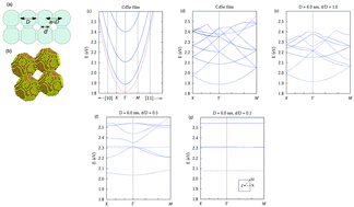
Two-dimensional films of semiconductors can be patterned into super-lattices with nanoscale periodicity, using top-down (lithography) or bottom-up approaches. In particular, square and honeycomb lattices of semiconductor nanocrystals have been recently synthesized using oriented attachment. We have performed atomistic tight-binding calculations of the conduction bands of super-lattices of CdSe. We consider spherical nanocrystals connected by horizontal cylinders and we investigate the band structure between two extreme limits, the uniform two-dimensional film, and the assembly of disconnected nanocrystals. Using this model system, we explain how rich band structures emerge from the periodic nano-geometry, including Dirac cones and non-trivial flat bands in honeycomb lattices. The possibility to build non-conventional band structures using multi-orbital artificial atoms (nanocrystals) opens up new prospects.

- This article is part of the themed collection: Fundamental Processes in Semiconductor Nanocrystals

 Please wait while we load your content...