Altering heating area assisted space confined method for growth of large scale and high quality MAPbBr3 single crystal thin films†
Abstract
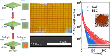
Metal halide perovskite materials exhibit remarkable optoelectronic properties due to their unique crystal and electronic structures. In perovskite polycrystalline films, the carrier transport is easily affected by grain boundaries where the defect density and stress are concentrated. Lacking grain boundaries, single crystals exhibit lower defect density, higher carrier mobility and longer carrier lifetime, thus benefiting longer carrier diffusion length. However, the large thickness of single crystals is not conducive to direct extraction of carriers out of photoelectric devices because the carrier diffusion length is within dozens of micrometers. Therefore, ultrathin single crystal films (SCFs) are demanded for photoelectric devices. In this paper, we put forward an improved space confined method, in which the nucleation and growth processes are controlled through altering the heating area. A series of MAPbBr3 SCFs with maximum size over 30 mm and controllable thickness (15–45 μm) are obtained. The growth kinetics of MAPbBr3 SCFs are analyzed in detail. Owing to the controllable growth kinetics, MAPbBr3 SCFs possess higher crystallinity, higher photo-induced carrier densities and longer carrier lifetimes than the corresponding bulk single crystals (BSCs). Therefore, MAPbBr3 SCFs exhibit better optoelectronic performance and device stability as planar photo-detectors, such as lower dark currents and higher photo-currents, higher R and EQE values and higher on/off ratios.


 Please wait while we load your content...