Sub-4 nm mapping of donor–acceptor organic semiconductor nanoparticle composition†
Abstract
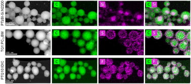
We report, for the first time, sub-4 nm mapping of donor : acceptor nanoparticle composition in eco-friendly colloidal dispersions for organic electronics. Low energy scanning transmission electron microscopy (STEM) energy dispersive X-ray spectroscopy (EDX) mapping has revealed the internal morphology of organic semiconductor donor : acceptor blend nanoparticles at the sub-4 nm level. A unique element was available for utilisation as a fingerprint element to differentiate donor from acceptor material in each blend system. Si was used to map the location of donor polymer PTzBI-Si in PTzBI-Si:N2200 nanoparticles, and S (in addition to N) was used to map donor polymer TQ1 in TQ1:PC71BM nanoparticles. For select material blends, synchrotron-based scanning transmission X-ray microscopy (STXM), was demonstrated to remain as the superior chemical contrast technique for mapping organic donor : acceptor morphology, including for material combinations lacking a unique fingerprint element (e.g. PTQ10:Y6), or systems where the unique element is in a terminal functional group (unsaturated, dangling bonds) and can hence be easily damaged under the electron beam, e.g. F on PTQ10 donor polymer in the PTQ10:IDIC donor : acceptor blend. We provide both qualitative and quantitative compositional mapping of organic semiconductor nanoparticles with STEM EDX, with sub-domains resolved in nanoparticles as small as 30 nm in diameter. The sub-4 nm mapping technology reported here shows great promise for the optimisation of organic semiconductor blends for applications in organic electronics (solar cells and bioelectronics) and photocatalysis, and has further applications in organic core–shell nanomedicines.


 Please wait while we load your content...