
Design considerations for the bottom cell in perovskite/silicon tandems: a terawatt scalability perspective†
 ‡*a
Bruno
Vicari Stefani,
‡b
Henry J.
Snaith,
d
Gregory J.
Wilson
b
and
Ruy Sebastian
Bonilla
a
‡*a
Bruno
Vicari Stefani,
‡b
Henry J.
Snaith,
d
Gregory J.
Wilson
b
and
Ruy Sebastian
Bonilla
a
Abstract
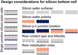
Perovskite/silicon tandems have smashed through the 30% efficiency barrier, which represents a promising step towards high efficiency solar modules. However, the processing used to fabricate high efficiency devices is not compatible with mass production. For this technology to be impactful in the urgent fight against climate change and be scalable to the multi-terawatt (TW) level, a shift in mindset is required when designing the silicon bottom cell. In this work, we outline the design requirements for the silicon cell, with a particular focus on the constraints imposed by industrial processing. In doing so, we discuss the type of silicon wafers used, the surface treatment, the most appropriate silicon cell architecture and the formation of metal contacts. Additionally, we frame this discussion in the context of multi-TW markets, which impose additional constraints on the processing relating to the sustainability of the materials used. The discussion herein will help to shape the design of future silicon solar cells for use in tandems, so that the LCOE of solar electricity can be driven to new lows.
 Please wait while we load your content...

