Single-crystalline lead halide perovskite wafers for high performance photodetectors†

Abstract
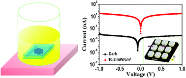
Lead halide perovskites are promising optoelectronic materials due to their unique properties such as strong light absorption, high carrier mobility, easily tunable bandgap, and compatibility with solution processable techniques. Most of the perovskite photodetectors are made of polycrystalline films, which are inferior due to large defective grain boundaries with respect to their single-crystalline (SC) counterparts. We have successfully grown SC lead halide perovskite wafers as large as 10 mm by combining the space-confined growth and seed-induced crystallization methods. In contrast, the single space-confined growth method only produces multiple SCs with sizes smaller than 3 mm. Due to the absence of grain-boundaries, the trap density of the prepared large SC perovskite wafer is only 2.36 × 1010 cm−3, much lower than that of polycrystalline thin films. The photodetectors based on the SC perovskite wafer with excellent crystalline quality show a light on/off current ratio of 4.3 × 10³, a response time of 770 μs, and a linear dynamic range of 119 dB. At the lowest detectable illumination power density of 80 nW cm−2, the prepared photodetector shows the highest external quantum efficiency, responsivity and detectivity of 904%, 3.87 A W−1, and 1.77 × 10¹³ Jones, respectively. Moreover, a natural SC perovskite device without any modification possesses good stability with its photocurrent maintained above 80% of its original value after 30 days of storage in air. The results indicate that high-performance photodetectors based on SC perovskite wafers may become competitive in future semiconductor information applications.
 Please wait while we load your content...

