Large-area high-quality graphene on Ge(001)/Si(001) substrates
Abstract
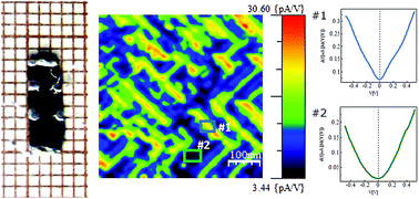
Various experimental data revealing large-area high-quality graphene films grown by the CVD method on Ge(001)/Si(001) substrates are presented. SEM images have shown that the structure of nano-facets is formed on the entire surface of Ge(001), which is covered by a graphene layer over the whole macroscopic sample surface of 1 cm2. The hill-and-valley structures are positioned 90° to each other and run along the <100> direction. The hill height in relation to the valley measured by STM is about 10 nm. Raman measurements have shown that a uniform graphene monolayer covers the nano-facet structures on the Ge(001) surface. Raman spectroscopy has also proved that the grown graphene monolayer is characterized by small strain variations and minimal charge fluctuations. Atomically resolved STM images on the hills of the nanostructures on the Ge(001) surface have confirmed the presence of a graphene monolayer. In addition, the STS/CITS maps show that high-quality graphene has been obtained on such terraces. The subsequent coalescence of graphene domains has led to a relatively well-oriented large-area layer. This is confirmed by LEED measurements, which have indicated that two orientations are preferable in the grown large-area graphene monolayer. The presence of large-area coverage by graphene has been also confirmed by low temperature Hall measurements of a macroscopic sample, showing an n-type concentration of 9.3 × 1012 cm−2 and a mobility of 2500 cm2 V−1 s−1. These important characteristic features of graphene indicate a high homogeneity of the layer grown on the large area Ge(001)/Si(001) substrates.


 Please wait while we load your content...