Large-area synthesis of monolayer WSe2 on a SiO2/Si substrate and its device applications
Abstract
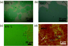
Recently two-dimensional layered semiconductors with promising electronic and optical properties have opened up a new way for applications in atomically thin electronics and optoelectronics. Here we report a large-area growth of monolayer WSe2 directly on SiO2/Si substrates by a chemical vapor deposition (CVD) method under atmospheric pressure. A sub-cooling step was demonstrated to have a key role in achieving this large-area growth. The monolayer configuration of the as-grown WSe2 was proven by spherical-aberration-corrected high resolution scanning transmission electron microscopy (HRSTEM), atomic force microscopy (AFM), Raman spectroscopy and photoluminescence (PL) spectroscopy. P-type behavior of as-grown monolayer WSe2 with a mobility of ∼0.2 cm2 V−1 s−1 and a carrier concentration of 1.11 × 1018 cm−3 was confirmed using back-gated field effect transistor (FET) devices. This large-area growth directly on a SiO2/Si substrate provides a new way to meet the industrial manufacturing requirements.


 Please wait while we load your content...