Probing photo-carrier collection efficiencies of individual silicon nanowire diodes on a wafer substrate†
Abstract
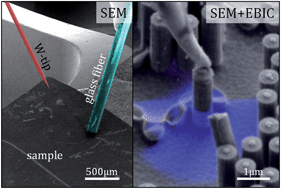
Vertically aligned silicon nanowire (SiNW) diodes are promising candidates for the integration into various opto-electronic device concepts for e.g. sensing or solar energy conversion. Individual SiNW p–n diodes have intensively been studied, but to date an assessment of their device performance once integrated on a silicon substrate has not been made. We show that using a scanning electron microscope (SEM) equipped with a nano-manipulator and an optical fiber feed-through for tunable (wavelength, power using a tunable laser source) sample illumination, the dark and illuminated current–voltage (I–V) curve of individual SiNW diodes on the substrate wafer can be measured. Surprisingly, the I–V-curve of the serially coupled system composed of SiNW/wafers is accurately described by an equivalent circuit model of a single diode and diode parameters like series and shunting resistivity, diode ideality factor and photocurrent can be retrieved from a fit. We show that the photo-carrier collection efficiency (PCE) of the integrated diode illuminated with variable wavelength and intensity light directly gives insight into the quality of the device design at the nanoscale. We find that the PCE decreases for high light intensities and photocurrent densities, due to the fact that considerable amounts of photo-excited carriers generated within the substrate lead to a decrease in shunting resistivity of the SiNW diode and deteriorate its rectification. The PCE decreases systematically for smaller wavelengths of visible light, showing the possibility of monitoring the effectiveness of the SiNW device surface passivation using the shown measurement technique. The integrated device was pre-characterized using secondary ion mass spectrometry (SIMS), TCAD simulations and electron beam induced current (EBIC) measurements to validate the properties of the characterized material at the single SiNW diode level.


 Please wait while we load your content...