Interface engineering of a highly sensitive solution processed organic photodiode†
Abstract
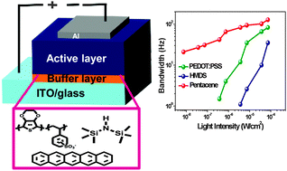
We report on tuning of the interfacial properties of a highly sensitive organic photodiode by introducing a buffer layer between the anode and the semiconductor layer. The effects of different buffer layers consisting of a self-assembled monolayer (SAM), PEDOT:PSS, and pentacene on the morphology and crystallinity of the upper-deposited bulk heterojunction semiconductor layer are carefully analyzed combined with electrical analysis. The active layer is controlled to be nearly homogeneous and to have low crystallinity by using a SAM or PEDOT:PSS buffer layers, whereas a highly crystalline morphology is realized by using the pentacene buffer layer. When exposed to light pulses, the external quantum efficiency and thus the photocurrent are slightly higher for the PEDOT:PSS-based photodiode; however the dark current is the lowest for the pentacene-based photodiode. We discuss the origin of the high sensitivity (a detectivity of 1.3 × 10¹² Jones and a linear dynamic range of 95 dB) of the pentacene-based photodiode, particularly in terms of the morphology-driven low dark current.
 Please wait while we load your content...

