DOI:
10.1039/D5YA00353A
(Paper)
Energy Adv., 2026,
5, 741-753
Enhancing stability and efficiency in perovskite solar cells: insights into inorganic HTL deposition and interface defect passivation
Received
2nd December 2025
, Accepted 4th March 2026
First published on 16th March 2026
Abstract
The perovskite solar cell (PSC) as an emerging and promising type of solar cell has been extensively studied, but instability is still a major challenge. Replacing the hygroscopic organic hole transport layer (HTL) in PSCs can result in an improvement in the device stability. However, it is still difficult to deposit inorganic HTLs onto the underlying perovskite layer without eroding or distorting it in the regular n–i–p architecture, thereby inducing defects at the interface and reducing the performance of the device. In this study, the performance of PSCs with an inorganic HTL is modelled using SCAPS-1D. The perovskite-HTL interface defect density was varied from 1.0 × 10¹² to 1.0 × 1020 cm−3. We realized that, for PSCs based on some hole transport materials (HTMs), the effect of interface defect density was not significant. We observed that the HTL/perovskite valence band offset (VBO) plays a significant role in the phenomenon observed. In particular, a zero or slightly positive VBO results in an increase in both the defect tolerance and device efficiency. This information provides insights into the fabrication of PSCs with improved interface defect passivation and also enables the fabrication of perovskite solar cells based on physically deposited inorganic charge transport materials.
1. Introduction
The rapid rise in the perovskite solar cell efficiency and the remarkable properties of perovskite solar cells, such as high absorption coefficient, long carrier diffusion length, tunable bandgap and simple production methods, have massively attracted researchers into this field, thereby leading to the achievement of a high efficiency close to the Shockley–Queisser limit.1,2 However, the stability of perovskite solar cell devices is still a major issue. The stability issues arise from internal and external factors, including moisture ingress due to the hygroscopic nature of the organic charge transport layers and the perovskite absorber, as well as thermal and photodegradation.3–5
These challenges have necessitated the search for alternative materials that will ensure the stability of solar cells, as stability is crucial to commercialization. To date, organic HTMs utilized in PSCs have demonstrated the highest efficiency.6 Nevertheless, the intrinsic low charge mobility and poor conductivity associated with pristine organic HTMs adversely impact the photovoltaic performance of PSCs. This is primarily due to increased series resistance and reduced recombination resistance. Dopants such as lithium bis(trifluoromethylsulphonyl)imide (Li-TFSI) and 4-tert-butylpyridine (TBP) are added to suppress charge recombination and improve the contact between the absorber and the HTM.7
Besides the hygroscopic nature of these organic dopants, the cost of doped hole transport materials (HTMs) is relatively high compared to their inorganic counterparts.8 Many strategies have been adopted to improve perovskite solar cell stability, including external encapsulation by lamination and internal passivation using organic or conductive polymers.9 Early perovskite devices without encapsulation showed stable operation up to hundreds of hours when stored in the dark and measured infrequently. However, these devices rapidly degraded after sustained exposure to sunlight.10 In addition to light exposure, elevated temperature and humidity may accelerate degradation due to moisture-induced decomposition of the perovskite crystals.11 These stability issues are being addressed through, for example, the use of protective coatings.12
The stability of perovskite PV devices under high humidity and temperature conditions has been improved by employing moisture-resistant layers (e.g., carbon nanotubes or graphite) to prevent water ingress.13–16 Improvements in device stability have also been achieved through encapsulation using glass or plastic lamination, with a stability of over 3000 hours at 60 °C being recorded.17 Furthermore, researchers have incorporated multiple cations, anions, and halides.18,19 This has led PSCs towards higher stability and efficiency compared to pure archetypical perovskites, which are typically composed of MAPbX3, FAPbX3, and CsPbX3 (X = Br or I). Rather than pure MAPbI3, mixed cation/halide perovskites, specifically those based on FAPbI3, contribute to a slight reduction in the optical bandgap. For example, the bandgap (Eg) of FAPbI3 is approximately 1.502 eV, whereas that of MAPbI3 is around 1.563 eV. This tailored bandgap, combined with the enhanced environmental stability of FAPbI3, results in improved performance of perovskite solar cells.17
While the addition of buffer layers or encapsulants increases device stability, it also adds to the cost and complexity. Another approach to improve PSC stability is replacing the hygroscopic organic hole transport layer with an inorganic HTL, which has been reported to be more stable than organic counterparts.20 A major challenge in depositing inorganic HTMs via solution methods onto the active layer in a regular PSC structure is the erosion of the underlying active layer by the inorganic HTM precursor solvent. Researchers have tried to deposit inorganic HTMs onto the perovskite layer and have achieved improved efficiency and stability, but the moisture from the deposition can create degradation pathways that deteriorate device performance over time.21 Depositing inorganic HTLs via the solution method remains challenging because the solvents that ensure good solubility for the inorganic HTL materials typically dissolve the underlying perovskite layer.22
Physical deposition methods could provide a better improvement in the device performance and better control of the process parameters to ensure repeatability. Researchers have tried physical deposition methods, but interface defects between the HTL and perovskite layers, resulting from these deposition processes, normally cause poor efficiency of the device.23 High-energy ions from this process normally distort the interface between the HTL and the perovskite, causing an increase in interface defects, thereby increasing the barrier to transport of holes from the absorber to the anode.24
To improve the solar cell performance by engineering the interface, emphasis has been placed on optimizing the HTM deposition process in order to minimize the interface defects for improved efficiency; however, a detailed understanding of the relationship between interface defects and other material properties and how these relationships consequently affect the performance of the solar cell is not well established. Thus, in this work, we focus on the material properties of different inorganic HTMs in order to understand the interplay of these properties and interfacial defects in relation to device performance. We investigated the effect of interface defects (Nit) on the efficiency of perovskite solar cell devices based on some inorganic HTLs by simulation using SCAPS 1D software.
The performance of perovskite solar cells is critically dependent on minimizing interface defects, which act as recombination centers. Emphasis is placed on the intrinsic band alignment between the perovskite absorber and the HTL, which plays a central role in modulating charge carrier recombination without relying on external chemical passivation strategies. In particular, a moderate positive VBO has been theoretically and experimentally linked to enhanced defect tolerance.25,26
2. Methodology
2.1. Solar cell structure for the study
The solar cell configuration for this study is FTO glass/compact TiO2/mesoporous TiO2/triple-cation (TC) perovskite absorber layer/inorganic HTMs/Au. In this n–i–p device structure, the perovskite layer light harvesting material is sandwiched between an n-type ETL (TiO2) and p-type HTL (Inorganic HTL) as shown in Fig. 1a, where the light passes through the ETL to reach the perovskite layer. The existence of the ETL and HTL in the PSC structure is essential because these layers play an important role in device performance by modifying the interface, adjusting the interfacial energy level, and enhancing the transport of photo-generated charge carriers to the electrodes, which in turn reduces the charge recombination.27,28 The energy band diagram consisting of the various materials considered for this study is shown in Fig. 1b.
 |
| | Fig. 1 (a) Perovskite solar cell architecture. (b) Energy band diagram. | |
2.2. Numerical simulation
Numerical analysis describes the basic phenomena present in photovoltaic devices, allowing intuitive examination of each parameter in solar cells and thus identifying the optimal conditions for operation.29 SCAPS-1D, a simulation software developed by the University of Ghent, Belgium, was used for this study. The simulation calculations conducted within SCAPS-1D are primarily based on two fundamental equations: the Poisson equation and the continuity equations for both electrons and holes.30| |  | (2.1) |
| |  | (2.2) |
| |  | (2.3) |
| |  | (2.5) |
| |  | (2.6) |
| |  | (2.7) |
Here, the symbols ε0 and εr represent the vacuum dielectric constant and the relative dielectric constant, respectively. The variables n and p denote the concentrations of free carriers, specifically electrons and holes. ND and NA signify the concentrations of donor and acceptor impurities, respectively. Additionally, ρn and ρp refer to the charge densities of electrons and holes, while Jn and Jp correspond to the current densities associated with electrons and holes. The parameter R represents the recombination rate for electrons and holes, respectively, whereas G denotes the generation rate of electrons or holes. ϕ symbolizes the electric field, and q refers to the electrical charge with a standard value of approximately 1.602 × 10⁻¹⁹ C. The mobilities of electrons and holes are represented by µn and µp, respectively. Dp and Dn stand for the diffusion coefficients for free holes and electrons, respectively. The variable υ represents the optical frequency, whereas A and B are arbitrary constants. Eg signifies the bandgap, h represents Planck's constant, and α(λ) is the absorption coefficient.
These simulations allow systematic tuning of one variable at a time or multiple variables simultaneously over a wide range that would otherwise be inaccessible experimentally. The simulation parameters in Tables 1–4 were obtained from previous reports. To accurately capture non-radiative losses originating at the heterojunctions, defect states were incorporated at both the ETL/perovskite and perovskite/HTL interfaces within the SCAPS-1D structure. In practical devices, interface defects can originate from lattice mismatch, surface roughness, incomplete surface coverage, and structural discontinuities formed during film crystallization. Termination of the perovskite lattice at the heterojunction often results in under-coordinated ions and dangling bonds, which introduce electronic trap states.31 Mechanical strain and mismatch between adjacent layers may further induce interfacial disorder and defect formation. Additionally, physical deposition processes, particularly sputtering of inorganic transport layers, can cause energetic particle bombardment damage, generating structural defects and increasing non-radiative recombination at the interface.32–34 These mechanisms predominantly introduce recombination-active trap centers that degrade the carrier lifetime and open-circuit voltage.
Table 1 Physical parameters of different layers used for the simulation30,46,49–51
| Parameters |
FTO |
TC perovskite |
TiO2 |
CuO |
CuSCN |
CuI |
CuAlO2 |
MoS2 |
CuSbS2 |
Cu2O |
| Band gap (eV) |
3.5 |
1.55 |
3.2 |
1.51 |
3.60 |
3.10 |
3.46 |
1.29 |
1.58 |
2.17 |
| Electron affinity (eV) |
3.3 |
3.9 |
4 |
4.07 |
1.7 |
2.1 |
2.50 |
4.2 |
4.20 |
3.2 |
| Dielectric permittivity |
9.0 |
6.6 |
9 |
18.1 |
6.5 |
7.11 |
60.00 |
8.9 |
14.6 |
10.7 |
| Conduction band effective density of states (cm−3) |
2.2 × 10¹⁸ |
1.0 × 10¹⁸ |
2.0 × 10¹⁸ |
2.2 × 10¹⁹ |
2.2 × 10¹⁹ |
2.8 × 10¹⁹ |
2.0 × 10²⁰ |
2.2 × 10¹⁸ |
2.0 × 10¹⁸ |
2.0 × 10¹⁷ |
| Valence band effective density of states (cm−3) |
1.8 × 10¹⁹ |
1.0 × 10¹⁸ |
1.8 × 10¹⁹ |
5.5 × 10²⁰ |
1.8 × 10¹⁸ |
1.0 × 10¹⁹ |
1.8 × 10²⁰ |
1.8 × 10¹⁹ |
1.0 × 10¹⁸ |
1.1 × 10¹⁹ |
| Electron mobility (cm2 V−1 s−1) |
2.0 × 10³ |
2 |
20 |
100 |
100 |
100 |
2 |
100 |
49 |
200 |
| Hole mobility (cm2 V−1 s−1) |
1.0 × 10² |
2 |
10 |
0.1 |
25.0 |
43.9 |
8.6 |
150.0 |
49 |
80 |
| Donor concentration (cm−3) |
2.0 × 10¹⁹ |
0 |
1.0 × 10¹⁸ |
|
|
|
|
|
|
|
| Acceptor concentration (cm−3) |
0 |
1.0 × 10¹⁵ |
0 |
1.0 × 10¹⁶ |
1.0 × 10¹⁸ |
1.0 × 10¹⁸ |
1.0 × 10¹⁹ |
1.0 × 10¹⁷ |
1.0 × 10¹⁹ |
1.0 × 10¹⁸ |
Table 2 Parameters for the contacts
| Contacts |
Anode properties |
Cathode properties |
| Metal work function (eV) |
5.1 |
4.4 |
| Surface recombination velocity of electrons (cm s−1) |
1.0 × 10⁷ |
1.0 × 10⁷ |
| Surface recombination velocity of holes (cm s−1) |
1.0 × 10⁷ |
1.0 × 10⁷ |
Table 3 Electrical properties of defects in the materials52,53
| Parameter |
Absorber |
ETL |
HTL |
| Defect type |
Neutral |
Single donor |
Single donor |
| Capture cross section for electrons (cm−2) |
1.0 × 10⁻¹⁵ |
1.0 × 10⁻¹³ |
1.0 × 10⁻¹⁴ |
| Capture cross section for holes (cm−2) |
1.0 × 10⁻¹⁵ |
1.0 × 10⁻¹⁴ |
1.0 × 10⁻¹³ |
| Energetic distribution |
Gauss |
Gauss |
Gauss |
| Energy level with respect to Ev |
0.6 (above Ev) |
1.2 (above Ev) |
0.65 (above Ev) |
| Defect density (cm−3) |
1 × 10¹⁵ |
1 × 10¹⁵ |
1 × 10¹⁵ |
Table 4 Electrical properties of defects at the interfaces52,53
| Parameter |
ETL/absorber |
Absorber/HTL |
| Defect type |
Neutral |
Neutral |
| Capture cross section for electrons (cm−2) |
1.0 × 10⁻¹⁹ |
1.0 × 10⁻¹⁹ |
| Capture cross section for holes (cm s−1) |
1.0 × 10⁻¹⁹ |
1.0 × 10⁻¹⁹ |
| Energetic distribution |
Single |
Single |
| Energy level with respect to Ev |
0.6 |
0.6 |
| Characteristic energy (eV) |
0.1 |
0.1 |
| Interface defect density (cm−2) |
1.0 × 10¹⁴ |
1.0 × 10¹² – 1.0 × 10²⁰ |
Although charged defect states may arise from ionized vacancies, anti-site defects, or interfacial chemical reactions, and can introduce fixed interfacial charge and band bending,31 the present study intentionally assumes neutral defect states. This modelling choice isolates recombination-dominated losses from electrostatic effects such as band alignment shifts or ion migration phenomena.35,36 By focusing on neutral recombination-active traps associated primarily with structural disorder rather than chemical degradation, the simulation framework enables direct evaluation of interface recombination sensitivity. This approach complements experimental passivation strategies aimed at chemically neutralizing charged defects and reducing trap densities. Consequently, the combined strategy of optimized band alignment and interface passivation provides a coherent pathway toward further enhancement of device performance.
We represent interface defects by a discrete deep trap level positioned 0.6 eV above the valence band maximum of the perovskite absorber. Deep-level traps located near the mid-gap are known to efficiently capture both electrons and holes, thereby accelerating SRH recombination.37 The electron and hole capture cross-sections were assigned values of 1 × 10⁻¹⁹ cm2, consistent with commonly reported simulation parameters for perovskite interfaces.37 These values represent moderate recombination velocity and allow systematic evaluation of recombination kinetics as a function of defect density. The interface defect density (Nti) was varied over a wide range of 1012–1020 cm−3 to represent different interface qualities, spanning well-passivated to severely damaged interfaces.
We varied Nti for different HTMs and the device I–V characteristics were recorded. The effect of other factors, including band offset, operating temperature, and acceptor concentration, was also investigated. This approach allows us to assess the importance of each material parameter to the final solar cell performance and to elucidate the limits beyond which power conversion efficiency decreases. The resulting insights are then used to guide new materials selection criteria and design processes.38
3. Results and discussion
3.1. Effect of interface defect density on the performance of the PSC for different inorganic HTMs
As shown in Fig. 2, variation in the interface defect density significantly affects the I–V characteristics of the devices based on Cu2O, CuSCN, or CuI. However, for devices based on CuO or MoS2, CuAlO2, and CuSbS2, it was observed that variation in the interface defects does not have a significant effect on the device characteristics, which indicates that the Nti is not the main influencing factor for the solar cells’ performance. As shown in Fig. 3 and Table 5, for the device based on CuSCN, the efficiency, Voc, Jsc and FF were reduced from 19.82%, 1.3 V, 23.3 mA cm−2, and 65.3%, respectively, to 14.93%, 1.14 V, 23.05 mA cm−2, and 56.96%, as the interface defect density was increased from 1 × 1012 cm−3 to 1 × 1020 cm−3. A similar trend is observed for the device based on CuI, where the efficiency, Voc, Jsc and FF decreased from 19.53%, 1.3 V, 23.3 mA cm−2, and 64.67%, respectively, to 12.62%, 1.09 V, 22.96 mA cm−2, and 50.5%. A similar trend is also observed for Cu2O. However, the devices based on CuO, MoS2, CuSbS2, and CuAlO2 exhibit insignificant changes in the I–V characteristics as the interface defect density increases from 1 × 1012 cm−3 to 1 × 1020 cm−3. In order to gain thorough insights into this tolerance behavior, we simulated the perovskite solar cell devices based on these HTMs by varying the material properties of the HTMs as shown in the following sections.
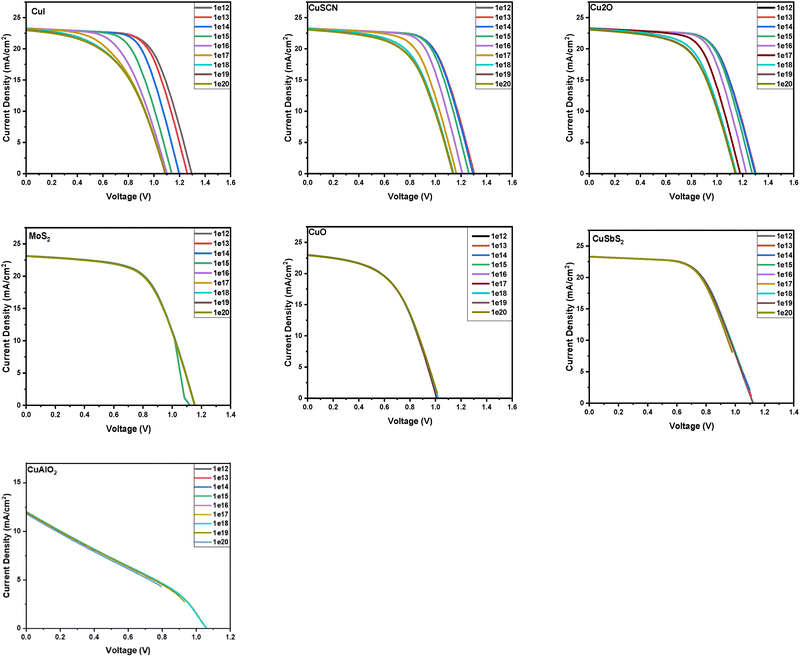 |
| | Fig. 2 Effect of interface defect density on the IV characteristics for different HTMs. | |
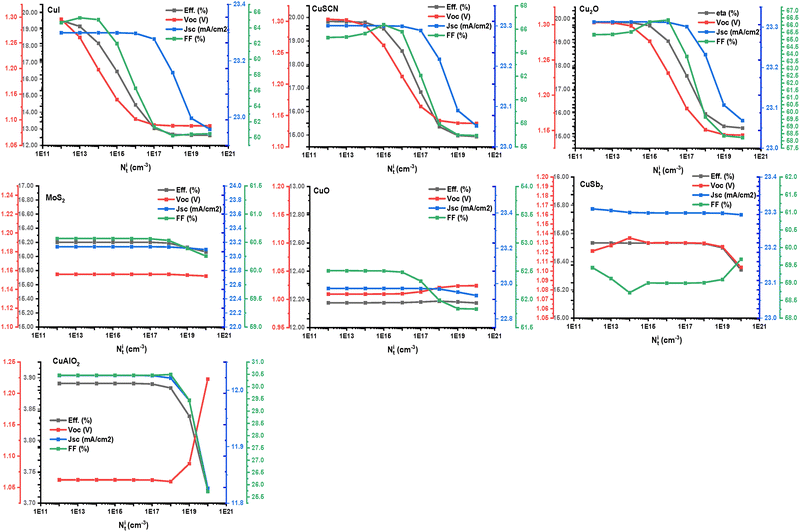 |
| | Fig. 3 Effect of interface defect density on the IV characteristics for different HTMs. | |
Table 5
I–V characteristics of the device based on various HTMs at 1012 cm−3 and 1020 cm−3
| HTMs |
N
t
i (cm−3) |
Eff. (%) |
V
oc (V) |
J
sc (mA cm−2) |
FF (%) |
| CuI |
1012 |
19.52986 |
1.29615 |
23.2996 |
64.66876 |
| 1020 |
12.61576 |
1.0882 |
22.95758 |
50.49864 |
| CuSCN |
1012 |
19.82882 |
1.30329 |
23.30042 |
65.29659 |
| 1020 |
14.93335 |
1.13738 |
23.05214 |
56.95612 |
| Cu2O |
1012 |
19.85439 |
1.3033 |
23.31324 |
65.34441 |
| 1020 |
15.3568 |
1.14322 |
23.06835 |
58.23095 |
| CuO |
1012 cm−3 |
12.17611 |
1.00944 |
22.97219 |
52.50784 |
| 1020 cm−3 |
12.17463 |
1.02433 |
22.93198 |
51.8292 |
| MoS2 |
1012 cm−3 |
16.20221 |
1.15612 |
23.1383 |
60.56765 |
| 1020 cm−3 |
16.06413 |
1.15421 |
23.09789 |
60.25573 |
| CuSbS2 |
1012 cm−3 |
15.53302 |
1.12128 |
23.30958 |
59.43031 |
| 1020 cm−3 |
15.34221 |
1.10391 |
23.29305 |
59.66596 |
| CuAlO2 |
1012 cm−3 |
3.89095 |
1.06214 |
12.02633 |
30.46078 |
| 1020 cm−3 |
3.72049 |
1.22288 |
11.8264 |
25.72541 |
3.2. Effect of valence band offset
As the movement of photo-generated charge carriers is typically affected by energy band alignment, the valence band offset can be calculated using the following equation.:39| | | VBO = (χHTL + Eg(HTL)) − (χabs + Eg(Abs.)) | (3.1) |
where χAbs and χHTL are the electron affinities of the absorber and HTL layers, respectively. Eg(Abs) and Eg(HTL) are the energy band gap values of the absorber and HTL layers, respectively.
The careful selection of the conduction band offset (CBO) and valence band offset (VBO) is essential for the effective transportation of photo-excited electrons and holes to the front electrode and back metal contact, respectively. This selection is critical for minimizing charge recombination within the absorber layer. The band offset can be modified by varying the electron affinity of the hole transport material (HTM) and electron transport material (ETM). In this study, our primary focus is on the effects of the VBO, as we are evaluating different HTMs. The band offsets are very important to define the barrier for transport of photo generated carriers from the absorber to the charge transport layers. Discontinuities at the interface generally play a crucial role in the charge transport phenomenon. Minority carriers are confronted with this barrier at the interface, favoring their accumulation and possibly causing recombination.40 The electron affinities of the electron transport layer (ETL) and the hole transport layer (HTL) are essential in establishing the energy level alignment between the absorber layer and the charge transport layers (CTLs). This alignment significantly influences the efficiency of perovskite solar cells by enabling the formation of interfaces that are conducive to effective charge transport. Nevertheless, the fundamental physical mechanisms and loss characteristics related to this energy-level alignment remain unclear. Specifically, the dynamic influence of the energy-level alignment with varying interface defect density has not been thoroughly investigated. In this context, we examined the influence of VBO on the interface defect tolerance of solar cells utilizing each of the HTMs chosen for this analysis. The values of Jsc, Voc and FF and the device efficiencies were recorded and are plotted in Fig. 4. The presence of cliffs and spikes at the edge of the absorber/HTL influences the performance of the specified solar cell. As illustrated in Fig. 5, a positive VBO indicates the formation of a spike near the interface between the absorber and the hole transport layer (HTL), which creates obstacles for the movement of hole charge carriers. In contrast, a negative VBO creates an energy cliff at the absorber/HTL interface, facilitating the movement of hole charge carriers.41Table 6 presents the computed valence band offsets (VBOs) for each hole transport layer in relation to the perovskite absorber layer, utilizing eqn (3.1). From Table 6, it is evident that Cu2O, CuI, and CuSCN exhibit a negative valence band offset (VBO), while CuO, MoS2, CuSbS2, and CuAlO2 show a positive VBO. The effect of the VBO is reflected in Fig. 6; devices with a negative VBO show a decrease in efficiency while those having a positive VBO exhibit a constant efficiency as Nti is increased from 1012 cm−3 to 1020 cm−3.
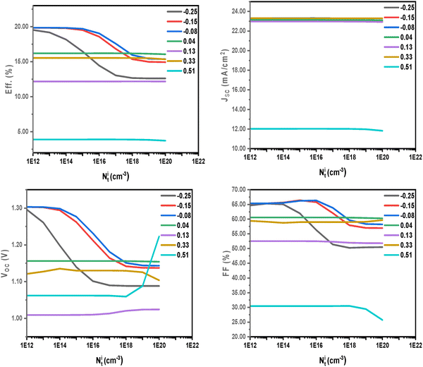 |
| | Fig. 4 Effect of interface defect density on the IV characteristics at different VBOs. | |
 |
| | Fig. 5 Schematics of cliffs and spikes in the valence band. | |
Table 6 Valence band offset at the Perovskite/HTL interface for devices based on various HTMs
| Material |
CuI |
CuSCN |
Cu2O |
MoS2 |
CuO |
CuSbS2 |
CuAlO2 |
| VBO |
−0.25 |
−0.15 |
−0.08 |
0.04 |
0.13 |
0.33 |
0.51 |
 |
| | Fig. 6 Energy band for the various inorganic HTM-based devices. | |
From Fig. 4, it was observed that the formation of a spike with a band offset of 0.04 eV provided beneficial effects, as reflected in the enhanced J–V characteristics and improved defect tolerance. We also noted that beyond certain thresholds above zero VBO, the efficiency of the devices begins to decrease.
Devices with moderate positive VBOs demonstrated superior open-circuit voltage (Voc), short-circuit current density (Jsc), and fill factor (FF) retention with increasing Nti. CuSbS2 and CuAlO2 retained their efficiency even at high Nti (∼1 × 1019 cm−3), validating the robustness of their band alignments. CuI and CuSCN showed steep efficiency drop-offs beyond Nti ∼ 1 × 1015 cm−3 due to higher recombination facilitated by less favorable Fermi level positioning. The small positive valence band offsets observed in the CuO, MoS2, CuSbS2, and CuAlO2 devices create a favorable energy barrier. This barrier slows hole transfer just enough to spatially separate charge carriers; this prevents backflow of holes into the perovskite, stabilizing charge separation, and thereby reducing recombination at the perovskite/HTM interface.23,42
The energy level diagram, which encompasses the electron transport layer (ETL), the perovskite absorber layer, and the HTL, is presented in Fig. 6. The quasi-Fermi levels for electrons (EF,n) and holes (EF,p) indicate the population distribution of photo-generated carriers under illumination. For HTLs with a positive VBO, the electron quasi-Fermi level EF,n stayed significantly separated from the valence band edge at the perovskite/HTL interfaces, as shown in Fig. 6. The significant separation of the EF,n from the conduction band edge of the perovskite, HTL and their interface is distinct from the negative VBO-based devices. An increase in the electron quasi-Fermi level typically indicates an increase in the concentration of photogenerated electrons. Therefore, the separation may imply a decrease in electron concentration at the perovskite/HTL interface region available for non-radiative recombination.30
As also observed in Fig. 6, the band bending induced by the positive VBO contributes to an electric field that repels electrons from the interface and attracts holes. This aids in spatial separation of carriers, reducing recombination and enabling defect states to remain electrically inactive.43,44
While negative VBOs (e.g., CuI, CuSCN, and Cu2O) promote seamless hole extraction, they may allow deeper penetration of holes into recombination-active regions. In contrast, HTMs with a positive valence band offset impede such penetration, thus reducing defect-assisted recombination. This illustrates the fundamental trade-off between transport facilitation and defect suppression that must be balanced in HTM selection.10,45 From the results obtained, it can be observed that MoS2 offers an optimal balance between effective hole extraction and recombination suppression.
3.3. The effect of acceptor concentration on I–V characteristics
As demonstrated, the materials with positive VBO exhibit high interface defect tolerance. However, their efficiencies are low compared to the devices based on negative valence band offset due to the interface barrier introduced by the spike formation at the interface, which obstructs carrier transport and increases recombination.
In order to optimize the efficiency of these devices, the effect of shallow acceptor density was analyzed by varying the acceptor densities of the HTMs in relation to the I-V characteristics of the devices. Fig. 7(a) and (b) show the results of the optimization, where the efficiency of the device based on CuO is increased from 12.18% to 18.68%. We selected CuO for the optimization because it has the lowest acceptor concentration used in the simulation. However, from the analysis, it can be seen that MoS2 exhibits the best performance, having shown high interface defect tolerance and higher efficiency when compared with other HTMs and at the same acceptor concentration. This is due to the fact that MoS2 possesses the least positive VBO, which enhances its charge transport.
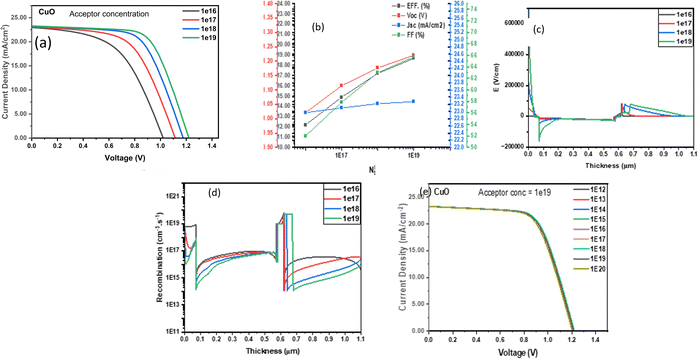 |
| | Fig. 7 (a) Effect of NA of the HTL on the I–V characteristics of the solar cell. (b) Effect of interface defects at higher acceptor concentration. (c) Electric field across the device layers. (d) Recombination rate across the device layers. (e) Effect of defect density on the device characteristics at 1 × 1019 cm−3 shallow acceptor concentration. | |
To investigate the cause of the increased efficiency with respect to shallow acceptor concentration, we studied the effect of an electric field on the device characteristics. From Fig. 7c, it can be observed that as the shallow acceptor concentration (NA) increases, the electric field at the CuO/perovskite interface increases. This increase in electric field facilitates the transport of charge carriers across the interface, hence the corresponding increase in efficiency at higher NA.46 This also corresponds to the decrease in recombination rate at increasing NA as shown in Fig. 7d. Furthermore, it can be seen that the increase in NA has an insignificant effect on the defect tolerance behavior of the device, as shown in Fig. 7e.
3.4. Effect of change in temperature
The bandgap changes at higher temperature, and thus the combined effect of temperature and defect density on the device characteristics was investigated. The results in Fig. 8 explain the interplay between bandgap changes at higher temperature during operation and the interface defects. The results show that irrespective of the temperature, the efficiency of the device follows a similar trend in relation to the interface defect density. For Cu2O (Fig. 8(a)), the efficiency plateaus up to Nti of 1 × 1015 cm−3 for all temperatures. This is followed by a sharp decrease in efficiency on further increase in the interface defect density. At higher temperature, the efficiency of the devices increases, but their responses to a change in interface defect density are similar. For MoS2 (Fig. 8(a)), the positive valence band offset induces interface defect tolerance that is unaffected by temperature change.
 |
| | Fig. 8 Effect of change in temperature on the I–V characteristics of the solar cell based on (a) Cu2O and (b) MoS2. | |
3.5. Effect of band gap and electron affinity on the device performance
As explained previously, the energy level alignment plays a crucial role in the stealth-like behavior of the interface defects. As the bandgap or electron affinity changes, one would expect the defect tolerance behavior to change. Therefore, we investigated this for the CuI and MoS2-based devices as shown in Fig. 9. It was observed that as the bandgap increases towards the formation of a positive VBO, there is the emergence and extension of a plateau region from 1 × 1012 cm−3 to 1 × 1016 cm−3. This plateau region is caused by the band alignment at higher bandgap, which is related to the defect tolerance effect. To further confirm this, we varied the electron affinity for two selected HTMs, MoS and CuI, while keeping the bandgap constant, and then studied their effects on defect passivation. The results confirm that the primary factor responsible for the defect tolerance in the devices based on these different HTMs is the valence band offset.
 |
| | Fig. 9
J–V characteristics of the CuI-based device with respect to interface defect density for (a) a change in electron affinity and (b) changes in bandgap. | |
3.6. Benchmarking against reported lead-based triple cation perovskite
To evaluate the realism of the simulated device performance, the optimized efficiency was compared with reported triple-cation (FA/Cs/MA) Pb-based mixed-halide perovskite solar cells, as shown in Table 7. Saliba et al. first demonstrated 21.1% efficiency using a Cs-containing triple-cation perovskite in a mesoporous architecture.47 Subsequent developments in compositional engineering and halide management have enabled efficiencies exceeding 22% in triple-cation Pb systems.48 In this context, the present simulated maximum efficiency of 19.85% for a triple-cation Pb perovskite employing a mesoporous TiO2 scaffold lies within the experimentally established performance envelope. The slightly lower efficiency compared to state-of-the-art certified devices may be attributed to conservative defect density assumptions and the absence of advanced interface passivation layers in the present model. This agreement supports the physical plausibility of the adopted recombination and material parameters.
Table 7 Benchmarking for a lead-based triple cation perovskite solar cell
| Composition |
Architecture |
Halide system |
PCE (%) |
Study type |
Ref. |
| FA/Cs/MA Pb(I/Br)3 |
n–i–p mesoporous |
I/Br |
21.1 |
Experimental |
Saliba et al.47 |
| FA/Cs/MA Pb(I/Br)3 |
Mesoporous |
I/Br |
19.5–20.1 |
Experimental |
Tan et al.54 |
| FA/Cs/MA Pb(I/Br)3 |
Optimized triple cation |
I/Br |
18–18.9 |
Experimental |
Conings et al.55 |
| FA/Cs/MA Pb(I/Br)3 |
Passivated triple cation |
I/Br |
19.21–21.71 |
Experimental |
Yang et al.56 |
| This work (FA/Cs/MA Pb mixed halide) |
Mesoporous TiO2 |
I/Br |
19.85 (Max) |
Simulation |
This work |
4. Conclusion
In this work, a comprehensive SCAPS-1D numerical investigation of a lead based mixed-cation perovskite solar cell was performed. Systematic optimization of absorber thickness, defect density, band alignment, transport layer selection, temperature, and parasitic resistances was conducted to evaluate performance sensitivity and defect tolerance. At moderate positive valence band offset, a stealth-like behavior of the interface defects is observed evidenced by the near constant efficiency with respect to an increase in interface defect density. The results indicate that the band alignment plays a crucial role in the device interface defect tolerance. This exposes the critical role of material selection in the reduction of the effect of interface defects on device performance. We also noted that the efficiency of the device based on the well aligned HTMs can be further optimized by tuning the material parameters of the HTMs.
The interface modelling framework adopted in this work isolates recombination-dominated losses arising from structurally induced interfacial defects (e.g., surface roughness or deposition damage), independent of electrostatic effects associated with charged defects. This approach enables quantitative assessment of recombination sensitivity and complements experimental passivation strategies. The results highlight that appropriate band alignment can intrinsically improve tolerance to interfacial defects, suggesting that materials selection and interface engineering are critical design parameters for high-efficiency lead-free perovskite solar cells. While record efficiencies for triple-cation Pb perovskites exceed 22% experimentally, the present simulation focuses on defect-limited behavior, providing insight into recombination-driven performance constraints rather than record-efficiency optimization.
The results provide insights that will guide material selection for the physical deposition of hole transport materials directly onto perovskite absorbers. Therefore, we conclude from our numerical results that appropriate band alignment in the inorganic HTL based n–i–p perovskite solar cell structure provides a certain level of tolerance to interface defects.
Author contributions
Conceptualization: Daniel I. Amune, E. Nstoenzok, and V. Anye. Methodology: Daniel I. Amune, E. Nstoenzok, V. Anye, R. Koech, Dahiru Sanni, W. Fidel, and J. Botsoa. Software: Daniel I. Amune. Validation: Daniel I. Amune, W. Fidel, R. Koech, and Dahiru Sanni. Funding acquisition: Daniel I. Amune and E. Nstoenzok. Data curation: Daniel I. Amune, E. Nstoenzok, and V. Anye. Formal analysis: Daniel I. Amune, E. Nstoenzok, W. Fidel, V. Anye, J. Botsoa, R. Koech, and Dahiru Sanni. Writing – original draft: Daniel I. Amune. Investigation: Daniel I. Amune. Supervision: E. Nstoenzok and V. Anye. Writing – reviewing and editing: Daniel I. Amune, E. Nstoenzok, V. Anye, J. Botsoa, R. Koech, and Dahiru Sanni.
Conflicts of interest
There are no conflicts to declare.
Data availability
Data for this article, including the effect of interface defect density on IV characteristics for different HTMs, the energy bands for the various inorganic HTM based devices, (a) the effect of NA of the HTL on the I–V characteristics of the solar cell, (b) the effect of interface defects at higher acceptor concentration, (c) the electric field across the device layers, (d) the recombination rate across the device layers, (e) the effect of defect density on the device characteristics at 1 × 1019 cm−3 shallow acceptor concentration, the effect of change in temperature on the I–V characteristics of the solar cell based on (a) Cu2O and (b) MoS2, and the J–V characteristics of the CuI-based device with respect to interface defect density for (a) a change in electron affinity and (b) changes in bandgap, are available at Harvard Dataverse Repository at https://doi.org/10.7910/DVN/VETUOV.
Acknowledgements
The authors acknowledge the funding from PASET – Regional Scholarship and Innovation Fund and JIRA project (RSIF/JIRA/003).
References
- T. Miyasaka, A. Kojima, T. Teshima and Y. Shirai, Organometal halide perovskites as visible-light sensitizers for photovoltaic cells, J. Am. Chem. Soc., 2009, 131(17), 6050–6051 CrossRef PubMed.
-
S. Ahmad, S. Kazim and M. Grätzel, Perovskite Solar Cells: Materials, Processes, and Devices, John Wiley & Sons, 2021 Search PubMed.
- U. Krishnan, M. Kaur, M. Kumar and A. Kumar, Factors affecting the stability of perovskite solar cells: a comprehensive review, J. Photonics Energy, 2019, 9(2), 21001 CAS.
- Y. Cheng and L. Ding, Pushing commercialization of perovskite solar cells by improving their intrinsic stability, Energy Environ. Sci., 2021, 14(6), 3233–3255 RSC.
- R. Wang, M. Mujahid, Y. Duan, Z. K. Wang, J. Xue and Y. Yang, A review of perovskites solar cell stability, Adv. Funct. Mater., 2019, 29(47), 1808843 CrossRef CAS.
- M. Saliba, T. Matsui, J. Y. Seo, K. Domanski, J. P. Correa-Baena and M. K. Nazeeruddin,
et al., Cesium-containing triple cation perovskite solar cells: Improved stability, reproducibility and high efficiency, Energy Environ. Sci., 2016, 9(6), 1989–1997 RSC.
- Z. H. Bakr, Q. Wali, A. Fakharuddin, L. Schmidt-Mende, T. M. Brown and R. Jose, Advances in hole transport materials engineering for stable and efficient perovskite solar cells, Nano Energy, 2017, 34, 271–305 CrossRef CAS.
- H. Zhou, Q. Chen, G. Li, S. Luo, T. Song and H. S. Duan,
et al., Interface engineering of highly efficient perovskite solar cells, Science, 2014, 345(6196), 542–546 CrossRef CAS.
- Q. Chen, H. Zhou, Y. Fang, A. Z. Stieg, T. B. Song and H. H. Wang,
et al., The optoelectronic role of chlorine in CH3NH3PbI3 (Cl)-based perovskite solar cells, Nat. Commun., 2015, 6(1), 7269 CrossRef CAS PubMed.
- G. Niu, X. Guo and L. Wang, Review of recent progress in chemical stability of perovskite solar cells, J. Mater. Chem. A, 2015, 3(17), 8970–8980 RSC.
- D. Yang, W. Ming, H. Shi, L. Zhang and M. H. Du, Fast diffusion of native defects and impurities in perovskite solar cell material CH3NH3PbI3, Chem. Mater., 2016, 28(12), 4349–4357 CrossRef CAS.
- J. J. Yoo, S. Wieghold, M. C. Sponseller, M. R. Chua, S. N. Bertram and N. T. P. Hartono,
et al., An interface stabilized perovskite solar cell with high stabilized efficiency and low voltage loss, Energy Environ. Sci., 2019, 12(7), 2192–2199 RSC.
-
Q. Luo, R. Wu, L. Ma, C. Wang, H. Liu, H. Lin, et al., Recent Advances in Carbon Nanotube Utilizations in Perovskite Solar Cells, Advanced Functional Materials, Wiley-VCH Verlag, 2021, vol. 31 Search PubMed.
- V. Ferguson, S. R. P. Silva and W. Zhang, Carbon Materials in Perovskite Solar Cells: Prospects and Future Challenges, Energy Environ. Mater., 2019, 2(2), 107–118 CrossRef CAS.
- J. Zhang, J. Fan, B. Cheng, J. Yu and W. Ho, Graphene-based materials in planar perovskite solar cells, Solar RRL, 2020, 4(11), 2000502 CrossRef CAS.
- S. Pandey, M. Karakoti, D. Bhardwaj, G. Tatrari, R. Sharma and L. Pandey,
et al., Recent advances in carbon-based materials for high-performance perovskite solar cells: gaps, challenges and fulfillment, Nanoscale Adv., 2023, 5(6), 1492–1526 RSC.
- K. Kranthiraja, M. Parashar, R. K. Mehta, S. Aryal, M. Temsal and A. B. Kaul, Stability and degradation in triple cation and methyl ammonium lead iodide perovskite solar cells mediated via Au and Ag
electrodes, Sci. Rep., 2022, 12(1), 18574 CrossRef CAS PubMed.
- N. J. Jeon, J. H. Noh, Y. C. Kim, W. S. Yang, S. Ryu and S. I. Seok, Solvent engineering for high-performance inorganic–organic hybrid perovskite solar cells, Nat. Mater., 2014, 13(9), 897–903 CrossRef CAS PubMed.
- K. A. Bush, K. Frohna, R. Prasanna, R. E. Beal, T. Leijtens and S. A. Swifter,
et al., Compositional engineering for efficient wide band gap perovskites with improved stability to photoinduced phase segregation, ACS Energy Lett., 2018, 3(2), 428–435 CrossRef CAS.
- H. S. Kim, I. Mora-Sero, V. Gonzalez-Pedro, F. Fabregat-Santiago, E. J. Juarez-Perez and N. G. Park,
et al., Mechanism of carrier accumulation in perovskite thin-absorber solar cells, Nat. Commun., 2013, 4(1), 2242 CrossRef PubMed.
- P. Kung, M. Li, P. Lin, Y. Chiang, C. Chan and T. Guo,
et al., A Review of Inorganic Hole Transport Materials for Perovskite Solar Cells, Adv. Mater. Interfaces, 2018, 5(22), 1800882 CrossRef.
- H. Tan, A. Jain, O. Voznyy, X. Lan, F. P. de Arquer and J. Z. Fan,
et al., Efficient and stable solution-processed planar perovskite solar cells via contact passivation, Science, 2017, 355(6326), 722–726 CrossRef CAS PubMed.
- E. Aydin, C. Altinkaya, Y. Smirnov, M. A. Yaqin, K. P. S. Zanoni and A. Paliwal,
et al., Sputtered transparent electrodes for optoelectronic devices: Induced damage and mitigation strategies, Matter, 2021, 4(11), 3549–3584 Search PubMed.
- Z. Song, S. C. Watthage, A. B. Phillips and M. J. Heben, Pathways toward high-performance perovskite solar cells: review of recent advances in organo-metal halide perovskites for photovoltaic applications, J. Photonics Energy, 2016, 6(2), 22001 Search PubMed.
- K. A. Bush, S. Manzoor, K. Frohna, Z. J. Yu, J. A. Raiford and A. F. Palmstrom,
et al., Minimizing current and voltage losses to reach 25% efficient monolithic two-terminal perovskite–silicon tandem solar cells, ACS Energy Lett., 2018, 3(9), 2173–2180 CrossRef CAS.
- T. Leijtens, G. E. Eperon, N. K. Noel, S. N. Habisreutinger, A. Petrozza and H. J. Snaith, Stability of metal halide perovskite solar cells, Adv. Energy Mater., 2015, 5(20), 1500963 CrossRef.
- D. N. Q. Agha and Q. T. Algwari, The influence of the conduction band engineering on the perovskite solar cell performance, Results Opt., 2022, 9, 100291 CrossRef.
- F. Wang, Y. Gao, Z. Pang, L. Yang and J. Yang, Insights into the role of the interface defects density and the bandgap of the back surface field for efficient p-type silicon heterojunction solar cells, RSC Adv., 2017, 7(43), 26776–26782 RSC.
- F. Wang, Y. Gao, Z. Pang, L. Yang and J. Yang, Insights into the role of the interface defects density and the bandgap of the back surface field for efficient p-type silicon heterojunction solar cells, RSC Adv., 2017, 7(43), 26776–26782 Search PubMed.
- A. Islam, S. Z. Haider, M. Wang, A. G. Ismail and H. Anwar, Interface engineering for improved performance of perovskite solar cells using CdTe buffer layer, Results Eng., 2024, 23 Search PubMed.
- Z. Wang, H. Gao, D. Wu, J. Meng, J. Deng and M. Cui, Defects and Defect Passivation in Perovskite Solar Cells, Molecules, 2024, 29, 2104 CrossRef CAS PubMed.
- X. Yan, J. Zheng, L. L. Zheng, G. Lin, H. Lin and G. Chen,
et al., Optimization of sputtering NiO x films for perovskite solar cell applications, Mater. Res. Bull., 2018, 103, 150–157, DOI:10.1016/j.materresbull.2018.03.027.
- M. Chen, D. Liu, C. You, X. Yang and Z. Cui, Interfacial characteristic of graded hydroxyapatite and titanium thin film by magnetron sputtering, Surf. Coat. Technol., 2007, 201, 5688–5691 CrossRef CAS.
-
L. C. Chen, J. C. Lin, K. L. Lee and Z. L. Tseng Sputtering and annealing graphene oxide hole-transporting layer for perovskite solar cells. In: 2018 7th International Symposium on Next Generation Electronics (ISNE) [Internet]. IEEE; 2018 [cited 2019 Aug 16]. p. 1–3. Available from: https://ieeexplore.ieee.org/document/8394628/.
- T. S. Sherkar, C. Momblona, L. Gil-Escrig, J. Ávila, M. Sessolo and H. J. Bolink,
et al., Recombination in Perovskite Solar Cells: Significance of Grain Boundaries, Interface Traps, and Defect Ions, ACS Energy Lett., 2017, 2(5), 1214–1222 Search PubMed.
- C. H. Peng and Y. C. Lin, SCAPS-1D Simulation of Various Hole Transport Layers’ Impact on CsPbI2Br Perovskite Solar Cells Under Indoor Low-Light Conditions, Solids, 2025, 6(3), 31 CrossRef CAS.
- M. S. Chowdhury, S. A. Shahahmadi, P. Chelvanathan, S. K. Tiong, N. Amin and K. Techato,
et al., Effect of deep-level defect density of the absorber layer and n/i interface in perovskite solar cells by SCAPS-1D, Results Phys., 2020, 16, 102839 CrossRef.
- R. Woods-Robinson, A. N. Fioretti, J. Haschke, M. Boccard, K. A. Persson and C. Ballif, Evaluating Materials Design Parameters of Hole-Selective Contacts for Silicon Heterojunction Solar Cells, IEEE J. Photovolt., 2021, 11(2), 247–258 Search PubMed.
- R. Ranjan, N. Anand, M. N. Tripathi, N. Srivastava, A. K. Sharma and M. Yoshimura,
et al., SCAPS study on the effect of various hole transport layer on highly efficient 31.86\% eco-friendly CZTS based solar cell, Sci. Rep., 2023, 13(1), 18411 Search PubMed.
- I. Sankara, S. Ouédraogo, D. Oubda, B. Traoré, M. B. Kébré and A. Zongo,
et al., Influence of Defect Density, Band Gap Discontinuity and Electron Mobility on the Performance of Perovskite Solar Cells, Adv. Mater. Phys. Chem., 2023, 13(8), 151–160 CrossRef CAS.
- Q. Chen, Y. Ni, X. Dou and Y. Yoshinori, The Effect of Energy Level of Transport Layer on the Performance of Ambient Air Prepared Perovskite Solar Cell: A SCAPS-1D Simulation Study, Crystals, 2022, 12(1), 68 Search PubMed.
- B. Chen, M. Yang, X. Zheng, C. Wu, W. Li and Y. Yan,
et al., Impact of capacitive effect and ion migration on the hysteretic behavior of perovskite solar cells, J. Phys. Chem. Lett., 2015, 6(23), 4693–4700 CrossRef CAS PubMed.
-
N. Park, M. Grätzel, T. Miyasaka, K. Zhu and K. Emery Towards Stable and Commercially Available Perovskite Solar Cells, 1–22.
- Q. Wang and A. Abate, Strategies toward stable perovskite solar cells, Adv. Mater. Interfaces, 2018, 5(22), 1800264 CrossRef.
- W. Ke, C. C. Stoumpos, I. Spanopoulos, L. Mao, M. Chen and M. R. Wasielewski,
et al., Efficient lead-free solar cells based on hollow MASnI3 perovskites, J. Am. Chem. Soc., 2017, 139(41), 14800–14806 CrossRef CAS PubMed.
- K. Afridi, M. Noman and S. T. Jan, Evaluating the influence of novel charge transport materials on the photovoltaic properties of MASnI3solar cells through SCAPS-1D modelling, R Soc Open Sci., 2024, 11(1), 231202 CrossRef CAS PubMed.
- M. Saliba, T. Matsui, J. Y. Seo, K. Domanski, J. P. Correa-Baena and M. K. Nazeeruddin,
et al., Cesium-containing triple cation perovskite solar cells: Improved stability, reproducibility and high efficiency, Energy Environ. Sci., 2016, 9(6), 1989–1997 RSC.
-
J. P. Correa-Baena, M. Saliba, T. Buonassisi, M. Grätzel, A. Abate, W. Tress, et al. Promises and challenges of perovskite solar cells [Internet]. Available from: https://science.sciencemag.org/.
- S. Banik, A. Das, B. K. Das and N. Islam, Numerical simulation and performance optimization of a lead-free inorganic perovskite solar cell using SCAPS-1D, Heliyon, 2024, 10(1), e23985 CrossRef CAS PubMed.
- M. K. Hossain, A. A. Arnab, R. C. Das, K. M. Hossain, M. H. K. Rubel and M. F. Rahman,
et al., Combined DFT, SCAPS-1D, and wxAMPS frameworks for design optimization of efficient Cs2BiAgI6-based perovskite solar cells with different charge transport layers, RSC Adv., 2022, 12(54), 34850–34873 RSC.
- F. Izadi, A. Ghobadi, A. Gharaati, M. Minbashi and A. Hajjiah, Effect of interface defects on high efficient perovskite solar cells, Optik, 2021, 227 Search PubMed.
- F. Izadi, A. Ghobadi, A. Gharaati, M. Minbashi and A. Hajjiah, Effect of interface defects on high efficient perovskite solar cells, Optik, 2021, 227, 166061 CrossRef CAS.
- H. K. Ibrahim, A. M. A. Sabaawi and Q. T. Algwari, Study of defects in CH 3 NH 3 PbI 3 -based perovskite solar cells, IOP Conf. Ser. Mater. Sci. Eng., 2021, 1152(1), 012032 CrossRef.
- H. Tan, A. Jain, O. Voznyy, X. Lan, F. P. G. De Arquer and J. Z. Fan,
et al., Efficient and stable solution-processed planar perovskite solar cells via contact passivation, Science, 2017, 355(6326), 722–726 CrossRef CAS PubMed.
- B. Conings, A. Babayigit, M. T. Klug, S. Bai, N. Gauquelin and N. Sakai,
et al., A Universal Deposition Protocol for Planar Heterojunction Solar Cells with High Efficiency Based on Hybrid Lead Halide Perovskite Families, Adv. Mater., 2016, 28(48), 10701–10709 CrossRef CAS PubMed.
- G. Yang, H. Zhang, S. Li, Z. Ren, G. Fang and D. Lei,
et al., Enhanced efficiency and stability of triple-cation perovskite solar cells with CsPbIxBr3 − x QDs “surface patches.”, SmartMat, 2022, 3(3), 513–521 CrossRef CAS.
|
| This journal is © The Royal Society of Chemistry 2026 |
Click here to see how this site uses Cookies. View our privacy policy here. 
 Open Access Article
 This Open Access Article is licensed under a Creative Commons Attribution-Non Commercial 3.0 Unported Licence
 c,
Dahiru
Sanni
*d,
J.
Botsoa
b,
V.
Anye
ae and
E.
Nstoenzok
b
c,
Dahiru
Sanni
*d,
J.
Botsoa
b,
V.
Anye
ae and
E.
Nstoenzok
b


