
 Open Access Article
 This Open Access Article is licensed under a Creative Commons Attribution-Non Commercial 3.0 Unported Licence
Modeling the photovoltaic characteristics of Zr-doped TiO2 dye-sensitized solar cells by incorporating CNT@TiO2
Mohammad Reza
Mohammadi
 *a,
Masoumeh
Khamehchi
b and
Aida
Mohammadi
c
*a,
Masoumeh
Khamehchi
b and
Aida
Mohammadi
c
aDepartment of Chemistry, Universidad Técnica Federico Santa María, Avenida España, 1680, Valparaíso, Chile. E-mail: mohammad.mohammadi@usm.cl
bDepartment of Basic Sciences, Hamedan University of Technology, Hamedan, Iran
cDepartment of Chemical Engineering, Queen's University, Kingston, ON K7L3N6, Canada
First published on 27th November 2025
Abstract
Using a diffusion differential model, this paper presents models that have been developed to predict the photovoltaic characteristics of Zr-doped TiO2 dye-sensitized solar cells (DSSCs) by incorporating a CNT–TiO2 core–shell (CNT@TiO2) with mono- and double-layer photoanode configurations. The monolayer cells are composed of Zr-doped TiO2 nanoparticles with different molar concentrations of Zr, while the double-layer devices are composed of Zr-doped TiO2 nanoparticles with optimum Zr content (i.e., 0.025 mol%) as the under-layer and CNT@TiO2, with varying CNT weight content, as the over-layer. The model evaluates the impact of critical parameters, including Zr concentration, CNT@TiO2 content, operating temperature, and photoanode thickness, on the photovoltaic characteristics of the devices. The model predictions are validated, demonstrating their capability to accurately represent the photocurrent density–voltage behavior of the devices. Results indicate that the photocurrent density of monolayer DSSCs increases with increasing Zr content up to 0.025 mol% and then decreases with further increases in Zr molar percentage. Moreover, both photocurrent density and open-circuit voltage of the double-layer devices first increase with the introduction of CNT@TiO2 and then decrease, reaching the highest value at 0.025 wt%. It is found that high operating temperatures lead to a decrease in the open-circuit voltage for all photoanode thicknesses, while the photocurrent density first increases with an increase in operating temperature and then decreases with a further temperature increase, reaching a maximum at 30 °C. For monolayer DSSCs, photocurrent density increases with electrode thickness up to 15 µm, after which it declines. These findings present essential knowledge for optimizing the design and efficiency of DSSCs.
1. Introduction
Solar energy is a key solution for sustainable and eco-friendly development, playing a vital role in curbing the excessive use of fossil fuels. Traditional solar cells exhibit high efficiency; however, their production process is labor-intensive and costly, limiting their widespread adoption. To overcome these challenges, numerous studies have focused on developing cost-effective and efficient alternatives, such as dye-sensitized solar cells (DSSCs). The first DSSCs were developed by O’Regan and Grätzel1, achieving a record energy conversion efficiency of 14.7%.2 Improving energy conversion efficiency is critical for the successful commercialization of DSSCs. One effective strategy involves enhancing electrical properties of TiO2 by selective doping, which can significantly boost the photovoltaic performance of DSSCs. Several studies have investigated the doping of TiO2 with transition metals such as Ta, Nb, Li, Ni, Zr, and W.3–5 These modifications aim to enhance the electrochemical characteristics and charge transport. Liu et al.6 investigated the application of doped TiO2 electrodes in quantum dot solar cells. TiO2 sols were doped with antimony and zirconium. It was observed that the doping of TiO2 with Sb and Zr enhanced the charge transport of the electrodes, potentially enhancing the efficiency of the cells. The impact of W doping in TiO2 for DSSCs, with doping levels ranging from 0.1% to 5% was examined by Zhang et al.3 Doping improved the material's electronic properties, reducing charge recombination and enhancing electron lifetime, which significantly increases the short-circuit current density (JSC). The greatest efficiency (9.1%) was also achieved with 0.2% W doping, resulting in a 17% increase in JSC and a 20% improvement in efficiency compared to undoped DSSCs.Light scattering is another method utilized in DSSCs to enhance optical absorption. Because they trap incident light inside the electrode, double-layer structures, which incorporate a second light-harvesting layer, are frequently used to improve photocurrent density and boost cell performance. 1D nanostructures, including nanorods, nanotubes, and nanofibers, are widely employed as light-scattering materials to accomplish this. Furthermore, they show effective electron transport and lessen photo-injected electron recombination. At the same time, multi-walled carbon nanotubes (MWCNTs) have garnered a lot of interest due to their huge surface area and quick electron transfer kinetics, which may be useful in solar cell applications. It has been highlighted that by bridging nanoparticles, one-dimensional nanostructures such as CNTs can function as light-scattering components, improving electron transport inside the photoelectrode sheet.7,8 Jung et al.8 studied the impact of incorporating single-wall carbon nanotubes (SWCNTs) into TiO2 film electrodes. The modified cells exhibited an increase in JSC and a slight decrease in open-circuit voltage (VOC). This improvement in JSC is linked to improved light scattering and electrical conductivity, as well as to a high concentration of electrons in the conduction band. It has been reported that photoconversion can be doubled by incorporating SWCNTs into photoelectrochemical cells composed of TiO2.9 In comparison to pristine TiO2, the observations showed a shift in the Fermi level upon the introduction of SWCNTs. Jang et al.10 studied the effects of anchoring dye molecules on the photocurrent–voltage characteristics of devices by integrating acid-treated SWCNs–TiO2 films. The modified cells exhibited a 25% increase in JSC compared to unmodified cells. Kim et al.11 reported that the photocurrent–voltage properties of DSSCs were greatly enhanced by the addition of rutile-TiO2-modified MWNTs. In comparison to cells with pure TiO2 films, the JSC increased by 35%, while VOC remained constant.
Park et al.12 investigated sol–gel derived Zr/N-doped TiO2 photoelectrodes for DSSCs. A red shift in the absorption into the visible spectrum was a characteristic of all the doped nanoparticles. Due to increased dye loading, reduced charge recombination, and increased charge transport, it was shown that the DSSCs composed of 0.01 molar Zr/N-doped TiO2 had an efficiency of 12.62%. Many dopants, including Zr, alter the absorption and band edge of TiO2, resulting in DSSCs with enhanced efficiency. Despite having a similar valence shell structure to Ti, Zr-doped TiO2 has garnered considerable interest in DSSCs due to its ability to improve light absorption and charge transport efficiency. In another study, Moradzaman et al.13 reported that Zr-doping improves dye adsorption by increasing porosity, shifts light absorption to longer wavelengths by reducing the band gap, and enhances electron injection, resulting in a PCE of 6.81% for Zr-doped TiO2 compared to 6.17% for pure TiO2. Incorporating the CNT–TiO2 core–shell into the top layer of a double-layer electrode further improves light scattering and electron transport, achieving a maximum PCE of 8.19%, thereby demonstrating significant efficiency gains through optimized material design.
Although numerous experimental studies have investigated the photocurrent density behavior of DSSCs, there remains a need for a comprehensive prediction model specifically tailored to DSSCs incorporating both CNTs and Zr-doped TiO2 nanoparticles, a gap this work aims to fill. The previously reported models predominantly focus on DSSCs based on pristine TiO2 photoanodes.14–18 For instance, Aboulouard et al.18 proposed a diffusion model based on the diffusion of electrons within a porous TiO2 thin film. This model was used to evaluate the impact of operating temperature on the performance of DSSCs. The findings revealed that temperature significantly influences the solar cells’ open-circuit voltage (VOC) and overall efficiency. An equivalent circuit model for DSSCs has been developed by Warepam et al.19, providing an accurate representation and a good fit for the experimental J–V curves and Nyquist plots. Tayeb et al. presented a simulation model with the MATLAB/SIMULINK interface for photovoltaic systems.20 The model simulates the I–V and P–V characteristics of solar cells under various environmental conditions by incorporating the basic circuit equations of PV cells, taking into consideration temperature fluctuations and solar radiation. These characteristics were obtained for TiO2-, ZnO-, and SnO2-based DSSCs using N3 dye molecules as the sensitizer. According to the simulation data, several elements, such as semiconductor type and environmental conditions, have an impact on the maximum working performance of the PV modules.
In this work, a diffusion differential model presented previously14,16,17 is developed to predict the photovoltaic performance of mono- and double-layer Zr-doped TiO2 nanoparticle DSSCs using CNT@TiO2. Moreover, the results of the developed model are compared with those obtained experimentally.13 Finally, the impact of CNT@TiO2 content, Zr molar percentage, operating temperature, and photoanode thickness on the photovoltaic characteristics of devices is investigated. While this work does not present new materials or record-breaking efficiencies, it introduces a validated, lightweight modeling framework that accurately predicts the photovoltaic performance of Zr-doped TiO2/CNT@TiO2 DSSC architectures across a range of design parameters. This tool may accelerate experimental optimization and support rational photoanode design in applied DSSC research.
2. Theory
2.1. Diffusion differential model for monolayer DSSCs based on pristine TiO2
In order to provide a precise expression for the photocurrent density, this mathematical model was presented under steady-state conditions with an emphasis on electron diffusion within a porous TiO2 thin film.17 This model is instrumental in understanding the operational mechanisms of DSSCs. Several authors have utilized this model14,16 to investigate VOC as a function of thickness and light intensity. In addition, it was applied to study the impact of photoanode thickness on the maximum power point. The following diffusion differential equation describes the model: | (1) |
The trapping and de-trapping of electrons were not accounted for in eqn (1), as this effect is only significant under non-steady-state conditions.24 Under short-circuit conditions, electrons are efficiently collected as photocurrent, with no direct transfer to the Pt counter electrode. The boundary conditions are established as follows:
| n(0) = n0 | (2) |
 | (3) |
 | (4) |
 | (5) |
The electron density at the TiO2/substrate interface rises to n, when the DSSC functions with a potential difference V between the Fermi level of TiO2 and the redox potential of the electrolyte, establishing a boundary condition:
| n(0) = n | (6) |
Eqn (1) shows that another boundary condition at x = d stays constant. Eqn (1) can be solved to determine J in terms of V.
 | (7) |
Fig. 1 illustrates a schematic of the device with the boundary conditions of the workflow.
 | ||
| Fig. 1 DSSC schematic with the boundary conditions. | ||
2.2. Developing the diffusion differential model for monolayer Zr-doped TiO2 DSSCs
Since the photovoltaic performance of Zr doped-TiO2 DSSCs depends on Zr content,13 a model to predict the current density–voltage (J–V) properties of these devices is presented. The diffusion differential model considers different external and internal factors and can also predict J–V of a DSSC based on pristine TiO2. Herein, this model is developed for the photocurrent density of the DSSCs based on Zr-doped TiO2 nanoparticles. To achieve this, eqn (4) is modified as follows: | (8) |
| φ = aebνtanh(ν) | (9) |
2.3. Developing the diffusion differential model for double-layer Zr-doped TiO2 DSSCs containing a CNT–TiO2 core–shell
We introduce a model to predict the photocurrent density of double-layer DSSCs made of CNT@TiO2 as the over-layer and 0.025 mol% Zr-doped TiO2 nanoparticles as the under-layer. In the following, the developed diffusion differential model in the previous section is redeveloped for the photocurrent density of these devices. To do this, substituting eqn (9) in eqn (8) for ν = 0.025 mol%, eqn (8) is modified as follows: | (10) |
| φ′ = a′eb′ν′tanh(ν′) | (11) |
Eqn (9) and (11) appear to be suitable choices for two reasons. First, when ν(ν′) = 0, the developed model simplifies to the original model. Second, this developed model is well-defined for various values of ν(ν′).
Although the double-layer photoanode architecture consists of two distinct functional regions, a Zr-doped TiO2 under-layer and a CNT@TiO2 over-layer, the present modeling framework adopts an effective single-layer approximation to maintain tractability in the absence of layer-resolved experimental parameters. In the reference study by Moradzaman et al.,13 the total photoanode thickness is reported as approximately 14 µm, but the individual thicknesses of the under- and over-layers are not specified. Consequently, a fully resolved two-domain diffusion model with explicit internal boundary conditions would introduce significant uncertainty due to underdetermined transport parameters (e.g., layer-specific diffusion coefficients, electron lifetimes, and absorption profiles). To circumvent this limitation while preserving predictive accuracy, we retain the same diffusion differential equation (eqn (1)) and global boundary conditions (eqn (2)–(3)) applied at the FTO/TiO2 interface (x = 0) and the electrolyte/porous film interface (x = d) but incorporate the structural and functional effects of the bilayer design through the empirical correction functions φ and φ′ (eqn (9) and (11)). These functions are calibrated against experimental J–V data, and effectively encapsulate the combined influence of enhanced light scattering, improve electron percolation via CNT networks, and modify recombination dynamics introduced by the CNT@TiO2 over-layer. While a more rigorous treatment would involve solving separate diffusion equations in each sublayer with continuity of electron concentration and flux at the internal interface (x = d1), such an approach requires detailed knowledge of interfacial energetics and layer-specific transport properties that are not available in the current experimental dataset. Nevertheless, our effective-medium strategy is physically justified under the assumption that the Zr-doped TiO2 and CNT@TiO2 layers are sintered into a continuous, electronically connected network without insulating barriers, allowing the internal interface to behave as a smooth compositional transition rather than a sharp discontinuity. The model's high fidelity, demonstrated by a prediction error of only 3.7% against independent experimental data, validates this simplification as a pragmatic and effective means of capturing the essential physics of the double-layer architecture. Future work will aim to refine this approach by implementing a true two-region diffusion model once layer-resolved characterization data become accessible.
Although the model does not explicitly incorporate optical scattering physics, the empirical correction functions φ(ν) and φ′(ν′) implicitly account for the net enhancement in photocurrent due to light scattering, increased dye loading, and improved charge collection in the double-layer architecture, as these effects are inherently embedded in the experimental J–V data used for calibration.
3. Results and discussion
3.1. Photovoltaic characteristics of monolayer Zr-doped TiO2 DSSCs
We employ the developed diffusion differential model to predict the photocurrent density of DSSCs based on Zr-doped TiO2 nanoparticles. To achieve this, the experimental database reported by Moradzaman et al.13 is divided into two data sets: the training data set presented in Table 1 and the test data set shown in Table 2. The training data set is used to estimate the unknown parameter in eqn (8), and the test set is used to verify the developed model. All simulations were performed using Wolfram Mathematica 13 through the least squared method.| DSSC | Voltage (V) | Photocurrent density (mA cm−2) | DSSC | Voltage (V) | Photocurrent density (mA cm−2) |
|---|---|---|---|---|---|
| ZT25 | 0.1 | 15.55 | ZT25/CNT10 | 0.6 | 9.32 |
| ZT25 | 0.3 | 15.46 | ZT25/CNT10 | 0.7 | 0 |
| ZT25 | 0.4 | 15.37 | ZT25/CNT25 | 0.1 | 19.49 |
| ZT25 | 0.6 | 9.43 | ZT25/CNT25 | 0.4 | 18.76 |
| ZT25 | 0.7 | 1.004 | ZT25/CNT25 | 0.6 | 10.53 |
| ZT50 | 0.0 | 14.06 | ZT25/CNT25 | 0.7 | 0 |
| ZT50 | 0.2 | 14.06 | ZT25/CNT50 | 00.0 | 17.7 |
| ZT50 | 0.4 | 13.71 | ZT25/CNT50 | 0.2 | 17.6 |
| ZT50 | 0.6 | 8.7 | ZT25/CNT50 | 0.4 | 16.97 |
| ZT75 | 0.1 | 13.71 | ZT25/CNT50 | 0.6 | 10.79 |
| ZT75 | 0.3 | 13.71 | ZT25/CNT75 | 0.1 | 16.97 |
| ZT75 | 0.5 | 10.22 | ZT25/CNT75 | 0.3 | 16.65 |
| ZT100 | 0.0 | 11.44 | ZT25/CNT75 | 0.5 | 13.09 |
| ZT100 | 0.2 | 11.53 | ZT25/CNT75 | 0.7 | 0 |
| ZT100 | 0.3 | 11.53 | ZT25/CNT100 | 0.0 | 16.55 |
| ZT100 | 0.5 | 9.61 | ZT25/CNT100 | 0.2 | 15.92 |
| ZT100 | 0.6 | 5.35 | ZT26/CNT100 | 0.4 | 14.45 |
| ZT25/CNT10 | 0.0 | 18.33 | ZT25/CNT100 | 0.6 | 6.8 |
| ZT25/CNT10 | 0.2 | 18.33 | ZT25/CNT100 | 0.67 | 0 |
| ZT25/CNT10 | 0.4 | 17.7 |
| DSSC | Voltage (V) | Photocurrent density (mA cm−2) | DSSC | Voltage (V) | Photocurrent density (mA cm−2) |
|---|---|---|---|---|---|
| ZT0 | 0 | 14.67 | ZT100 | 0.1 | 11.62 |
| ZT0 | 0.1 | 14.67 | ZT100 | 0.4 | 11.27 |
| ZT0 | 0.2 | 14.94 | ZT25/CNT10 | 0.1 | 18.33 |
| ZT0 | 0.3 | 14.67 | ZT25/CNT10 | 0.3 | 18.33 |
| ZT0 | 0.4 | 14.41 | ZT25/CNT10 | 0.5 | 14.8 |
| ZT0 | 0.5 | 12.23 | ZT25/CNT25 | 0 | 19.39 |
| ZT0 | 0.6 | 8.3 | ZT25/CNT25 | 0.2 | 19.39 |
| ZT25 | 0 | 15.37 | ZT25/CNT25 | 0.3 | 19.28 |
| ZT25 | 0.2 | 15.55 | ZT25/CNT25 | 0.5 | 16.47 |
| ZT25 | 0.5 | 13.8 | ZT25/CNT50 | 0.1 | 17.7 |
| ZT50 | 0.1 | 14.15 | ZT25/CNT50 | 0.3 | 17.28 |
| ZT50 | 0.3 | 13.98 | ZT25/CNT50 | 0.5 | 15.19 |
| ZT50 | 0.5 | 12.58 | ZT25/CNT75 | 0 | 17.07 |
| ZT50 | 0.7 | 0.873 | ZT25/CNT75 | 0.2 | 16.86 |
| ZT75 | 0 | 13.71 | ZT25/CNT75 | 0.4 | 15.9 |
| ZT75 | 0.2 | 13.71 | ZT25/CNT75 | 0.6 | 8.38 |
| ZT75 | 0.4 | 12.75 | ZT25/CNT100 | 0.1 | 16.34 |
| ZT75 | 0.6 | 5.35 | ZT25/CNT100 | 0.3 | 15.4 |
| ZT75 | 0.68 | 0 | ZT25/CNT100 | 0.5 | 12.78 |
Moradzaman et al.13 prepared five different monolayer photoanode films, with an average thickness of 14 µm and various Zr mol% (i.e., 0, 0.25, 0.05, 0.075 and 0.1 mol%) and studied the impact of Zr dopant concentration on the photovoltaic performance of DSSCs. The devices were designated as ZT0, ZT25, ZT50, ZT75, and ZT100. The photovoltaic characteristics of the devices were measured at room temperature.
Based on the above information and the training data set presented in Table 1, the values of φ were determined by fitting the experimental data using eqn (8). Table 3 shows the φ values corresponding to each experimental dataset.
| DSSC | ν (mol%) | φ |
|---|---|---|
| ZT0 | 0 | 0 |
| ZT25 | 0.025 | −0.696 |
| ZT50 | 0.050 | 0.040 |
| ZT75 | 0.075 | 1.136 |
| ZT100 | 0.100 | 2.325 |
Considering Table 3 and eqn (9), the expression for φ as a function of the Zr-dopant percentage is derived as:
| 1.12e30.543νtanh(ν) | (12) |
It is seen that for ν = 0, the developed model is simplified to the original model. Moreover, this function is well-defined for various ν values.
The test dataset from Table 2 was employed to verify the model developed in the present study. Fig. 2 compares the predicted photocurrent density values with the corresponding experimental data from Table 2. It is evident that the proposed developed model can perfectly predict the photocurrent density of Zr-doped TiO2 DSSC, with an error of 4% compared with the test data set presented in Table 2.
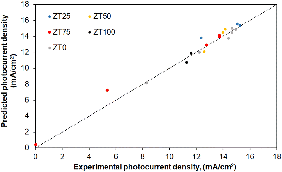 | ||
| Fig. 2 Experimental values compared to the model predictions for the photocurrent density of the monolayer Zr-doped TiO2 DSSCs with different Zr content. | ||
In the following, the impact of Zr content, operating temperature, and electrode thickness on the photocurrent density–voltage of monolayer DSSCs is evaluated based on the developed diffusion differential model.
Fig. 3 illustrates the impact of Zr molar percentage on the photocurrent density–voltage (J–V) characteristics of the DSSC based on Zr-doped TiO2 nanoparticles. We observe that JSC increases with an increase in Zr molar percentage up to 0.25 mol% and then decreases with further increase in Zr content. Therefore, the ZT25 cell demonstrates the highest JSC of 15.24 mA cm−2 among all the fabricated solar cells. This is due to the reduction in electrical resistance by modification of the electron/hole concentration and the formation of new energy levels within the TiO2 band gap upon Zr doping. However, doping Zr at more than 0.25%mol may cause defect formation due to the substitution of large Zr ions, resulting in decreasing JSC. Furthermore, the VOC of the cells composed of Zr-doped TiO2 nanoparticles is lower than that of pure TiO2. This can be explained by the difference between the redox potential of the electrolyte and the Fermi level, which decreases by doping Zr into TiO2 nanoparticles, resulting in increased recombination for Zr-doped TiO2 devices. Such a difference can be assigned to the crystal structure of the nanoparticles; the pure anatase structure for pure TiO2 and a combination of rutile and anatase phases for Zr-doped TiO2. These results are consistent with those reported by Moradzaman et al.13
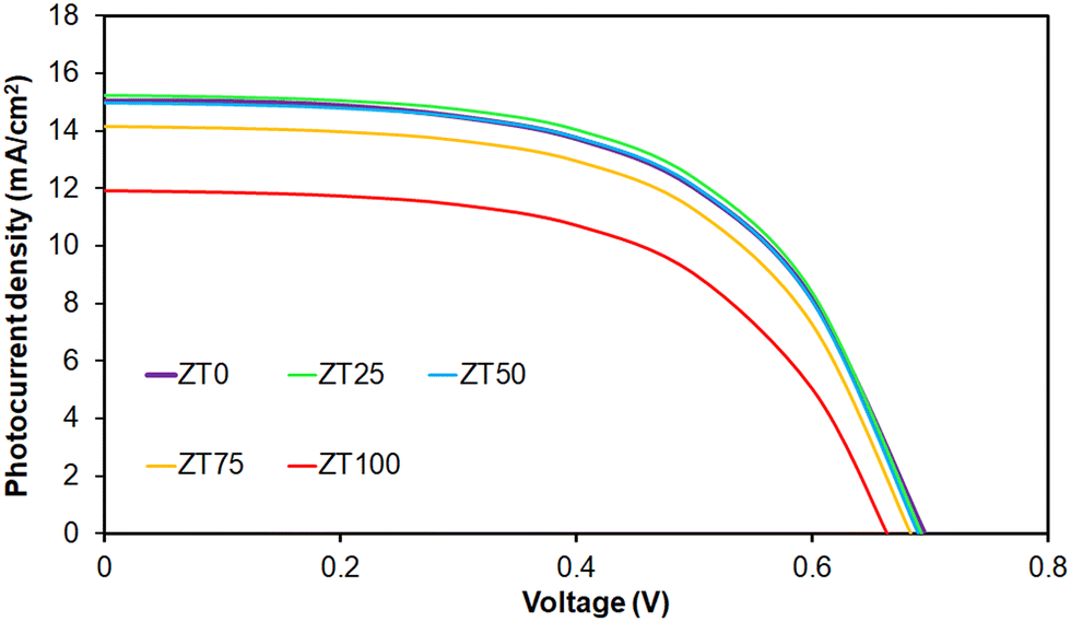 | ||
| Fig. 3 The impact of the Zr content on J–V curves of monolayer DSSCs based on the Zr-doped TiO2 nanoparticles. | ||
The photovoltaic parameters of monolayer Zr-doped TiO2 DSSCs obtained by the presented model are listed in Table 4 along with their experimental results. It is evident that the ZT25 cell exhibits the greatest power conversion efficiency (η) of 6.17%. The enhanced efficiency can be explained by the fact that the introduction of Zr creates extra energy levels within the TiO2 bandgap, resulting in enhanced photoresponse. By creating acceptor levels in the bandgap, the Zr dopant changes the electronic structure of TiO2, changing the concentrations of electrons and holes and lowering the internal electrical resistance.13
| DSSC | J SC,exp (mA cm−2) | J SC,model (mA cm−2) | V OC,exp (mV) | V OC,model (mV) | FFexp (%) | FFmodel (%) | η exp (%) | η model (%) |
|---|---|---|---|---|---|---|---|---|
| ZT0 | 14.6 | 14.98 | 732 | 696 | 57.6 | 57.5 | 6.17 | 6.01 |
| ZT25 | 15.5 | 15.24 | 712 | 692.3 | 62.6 | 58.5 | 6.81 | 6.17 |
| ZT50 | 14.2 | 14.06 | 706 | 690 | 62.4 | 58.4 | 6.21 | 6.03 |
| ZT75 | 13.7 | 14.13 | 688 | 683 | 56.2 | 58.2 | 5.27 | 5.62 |
| ZT100 | 11.5 | 11.91 | 680 | 663 | 61.7 | 57.1 | 4.80 | 4.51 |
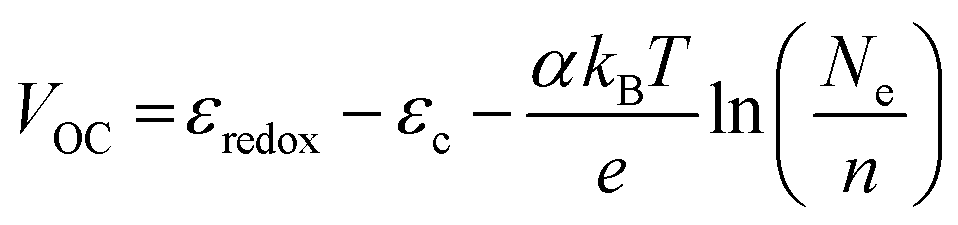
Fig. 4 presents the current density–voltage behavior of 0.025 mol% Zr-doped TiO2 DSSCs at various operating temperatures in the range of 10–40 °C and various photoanode thicknesses between 1 µm and 20 µm. We observed that, for all photoanode thicknesses, JSC slightly increased up to 30 °C and then decreased with further increase in operating temperature, while VOC decreased with increasing operating temperature. An increase in the JSC up to 30 °C can be related to the enhanced reaction kinetics of the electron injection and the improved diffusion rate of electrons and ions. The decrease in JSC at higher temperatures may be attributable to increased recombination, thermal degradation of materials, and loss of photogenerated electrons. The dependence of VOC on temperature can be attributed to the potential difference between the quasi-Fermi level, εF, at the FTO/Zr-doped TiO2 interface and the redox potential, εredox, at the counter electrode:
| VOC = εredox − εF | (13) |
 | (14) |
 | (15) |
 | ||
| Fig. 4 J–V characteristics of the 0.025 mol% Zr-doped TiO2 DSSCs (ZT25) under different operating temperatures and various photoanode thicknesses: (a) 10 µm, (b) 15 µm and (c) 20 µm. | ||
Furthermore, JSC increases with photoanode thickness up to about 15 µm, indicating that the optimal thickness is about 15 µm. Beyond this point, JSC begins to decrease. The observed variation in JSC can be attributed to electron photogeneration. For specific porosity and pore size, increasing the thickness of the electrode enhances the surface area, which, in turn, allows for greater dye sensitization. As a result, thick electrodes can absorb more photons, resulting in an increase in JSC. When the thickness exceeds the light penetration depth, the photons available for electron generation reach a saturation point, preventing further increases in JSC. Beyond this threshold, additional thickness introduces more recombination sites, which promote electron loss and consequently lead to a gradual decline in JSC.16
3.2. Photovoltaic characteristics of double-layer Zr-doped TiO2 DSSCs using a CNT–TiO2 core–shell
We redeveloped the diffusion differential model for double-layer DSSCs based on predicting their photocurrent density behavior. To do this, the training data set presented in Table 1 was used to estimate the unknown parameter in eqn (10), and the test set in Table 2 was used to evaluate the predictions of the developed model.Moradzaman et al.13 fabricated five different double-layer photoanode electrodes, composed of ZT25 (v = 0.025 mol%) in the under-layer and mixtures of CNT–TiO2 core–shell and ZT25 with various CNT contents (0.01, 0.025, 0.05, 0.075 and 0.1 wt%) in the top-layer, and studied the impact of CNT content on the photovoltaic performance of DSSCs. The cells were designated as ZT25/C10, ZT25/C25, ZT25/C50, ZT25/C75, and ZT25/C100. The photovoltaic characteristics of devices were measured at room temperature.
Based on the above information and the training data set presented in Table 1, the values of φ′ were determined by fitting the experimental data using eqn (10). Table 5 presents the φ′ values corresponding to each experimental dataset based on the CNTs content.
| DSSC | ν′ (wt%) | φ′ |
|---|---|---|
| ZT25/CNT10 | 0.010 | −2.220 |
| ZT25/CNT25 | 0.025 | −2.108 |
| ZT25/CNT50 | 0.050 | −1.902 |
| ZT25/CNT75 | 0.075 | −0.791 |
| ZT25/CNT100 | 0.100 | 0.249 |
Based on Table 5 and eqn (11), the explicit expression for φ′ as a function of CNT@TiO2 content is determined as follows:
| −322.650e−47.222ν′tanh(ν′) | (16) |
For ν′ = 0, the model reduces to the developed model in Section 3.1 for 0.025 mol% Zr-doped TiO2. Furthermore, this function is well-defined for a range of ν′ values.
The model developed in this study was validated using the test dataset presented in Table 2. Fig. 5 compares the predicted photocurrent density values and the corresponding experimental data from Table 2.
 | ||
| Fig. 5 Experimental values compared to the model predictions for the photocurrent density of the double-layer Zr-doped TiO2 DSSCs using CNT@TiO2. | ||
The proposed model shows excellent agreement, predicting the photocurrent density of the DSSC with only 3.7% error compared to the test dataset in Table 2. Using the redeveloped diffusion differential model, the following analysis evaluates the impact of CNT content and operating temperature on the photocurrent density–voltage of the double-layer DSSCs.
Fig. 6 illustrates the effect of CNT@TiO2 content on the J–V characteristics of the double-layer DSSCs. It is observed that double-layer DSSCs incorporating CNT@TiO2 and Zr-doped TiO2 nanoparticles exhibit higher JSC and VOC than the monolayer ZT25 device. For example, in comparison to ZT25, the photocurrent density increases by approximately 22.2%, 27.4%, 16.8%, 7.7%, and 3.1% for ZT25/CNT10, ZT25/CNT25, ZT25/CNT50, ZT25/CNT75, and ZT25/CNT100, respectively. Moreover, both the VOC and JSC of the DSSCs increase when the CNT@TiO2 content is increased to 0.025 wt%. However, a further increase in CNT@TiO2 content leads to a reduction of VOC and JSC. Consequently, the ZT25/CNT25 cell demonstrates the highest JSC, VOC and η of 18.82 mA cm−2, 0.712 mV and 7.96%, respectively, among all the double-layer cells. The photovoltaic enhancement of the double-layer DSSCs can be attributed to the enhanced visible-light scattering by the top layer film containing clusters formed due to the incorporation of CNT@TiO2 as well as to the improved electrical conductivity resulting from enhanced interconnectivity between the CNT@TiO2 and TiO2 particles.
 | ||
| Fig. 6 The impact of the CNT@TiO2 content on the J–V curves of the double-layer Zr-doped TiO2 DSSCs using CNT@TiO2. | ||
Table 6 lists the photovoltaic parameters of the double-layer DSSCs along with their experimentally measured values. We found that the proposed model shows excellent agreement with the experimental measurements, accurately predicting the photovoltaic parameters of the double-layer DSSCs with low errors. For example, the conversion efficiency of the ZT25/CNT25 cell, which exhibits the highest value among all the double-layer devices, is predicted to be 7.96% by the proposed model and measured at 8.19% experimentally, with an error of less than 3%. This improvement in cell efficiency is attributed to the designed architecture of the double-layer photoanode. The under-layer, composed of Zr-doped TiO2, exhibited low internal resistance and good porosity, enhancing dye sensitization. Furthermore, the CNT@TiO2 in the over-layer improved electron transport and light scattering, increasing the optical path length and providing a more direct electron pathway.13
| DSSC | J SC,exp (mA cm−2) | J SC,model (mA cm−2) | V OC,exp (mV) | V OC, model (mV) | FFexp (%) | FFmodel (%) | η exp (%) | η model (%) |
|---|---|---|---|---|---|---|---|---|
| ZT25 | 15.5 | 15.24 | 712 | 692 | 62.6 | 58.5 | 6.81 | 6.17 |
| ZT25/CNT10 | 18.3 | 18.15 | 725 | 716 | 57.3 | 59 | 7.49 | 7.62 |
| ZT25/CNT25 | 19.4 | 18.82 | 699 | 712 | 60.2 | 59.07 | 8.19 | 7.96 |
| ZT25/CNT50 | 17.8 | 17.44 | 715 | 715 | 59.6 | 58.9 | 7.57 | 7.27 |
| ZT25/CNT75 | 17.0 | 16.25 | 692 | 699 | 56.1 | 58.77 | 6.89 | 6.67 |
| ZT25/CNT100 | 16.6 | 15.65 | 663 | 694 | 57.0 | 58.70 | 6.30 | 6.37 |
Fig. 7 shows the J–V characteristics of the double-layer DSSCs based on CNT@TiO2 and Zr-doped TiO2 nanoparticles under different operating temperatures ranging from 10 °C to 40 °C for a photoanode electrode with a thickness of 14 µm. It is realized that the JSC slightly increased up to 30 °C and then decreased with further increases in operating temperature, while VOC decreased with an increase in operating temperature. Basically, the short-circuit current density initially increases with temperature up to 30 °C due to enhanced charge mobility. However, as the temperature continues to rise beyond 30 °C, the increase in recombination and the potential degradation of the electrolyte cause JSC to decrease. Moreover, the open-circuit voltage decreases with an increase in operating temperature because higher temperatures reduce the energy difference between the electrons in the conduction band and the redox potential of the electrolyte, leading to a lower VOC.
 | ||
| Fig. 7 The photocurrent density–voltage characteristics of the double-layer Zr-doped TiO2 DSSCs using CNT@TiO2 at various operating temperatures. | ||
Based on Fig. 1–7, we concluded that the developed model presented in this study effectively predicts the J–V characteristics of the mono- and double-layer DSSCs.
Overall, using Mathematica as a powerful computational tool, this study introduces a novel DSSC modeling framework that surpasses existing diffusion models through two distinct device architectures: monolayer DSSCs composed of Zr-doped TiO2 nanoparticles and double-layer Zr-doped TiO2 DSSCs incorporating a CNT–TiO2 core–shell. The findings provide a validated theoretical basis for DSSC optimization, bridging the gap between computational predictions and experimental performance. A systematic comparison between monolayer and double-layer DSSCs was also conducted under various conditions. The developed model predicts the photovoltaic characteristics of both device architectures with much greater precision than numerical simulations previously reported by SCAPS, AMPS, and COMSOL.26,27 It also predicts the impact of different key parameters, including Zr concentration, CNT@TiO2 content, operating temperature, and photoanode thickness on the photovoltaic behavior of Zr-doped TiO2 DSSCs by incorporating CNT@TiO2. Having considered the pitfalls when reporting calculated photovoltaic parameters presented by Morales-Acevedo,26 it is found that our model explicitly considers various parameters, including the concentration of photo-generated electrons, equilibrium electron concentration in the dark, electron diffusion coefficient, light intensity, electrode light absorption coefficient, photoanode thickness, and electron diffusion length. In addition, unlike the previous model reported by Kuddus et al.,27 our approach, which incorporates experimental measurements in the calculations, indirectly accounts for the synergistic effects of Zr doping and CNT integration on charge transport, as well as the impact on recombination dynamics. The developed model demonstrates enhanced predictive accuracy when validated against experimental data, achieving an error of less than 4%. Moreover, the predicted photovoltaic parameters are compared with experimental data measured in the lab, showing that the developed model not only achieves good agreement with existing data but also successfully predicts the photovoltaic characteristics of the devices within the limits established by the Shockley–Queisser theory.28
It should be noted that the primary objective of this study is to develop a predictive diffusion-based model for the J–V characteristics of mono- and double-layer Zr-doped TiO2 DSSCs incorporating CNT@TiO2, with a focus on reproducing experimentally observed trends in JSC, VOC, FF, and efficiency under variations in Zr content, CNT loading, temperature, and thickness. While parameters such as reverse saturation current (J0), maximum power point coordinates, and interfacial resistances are valuable for detailed device diagnostics, they are not explicitly calculated in this framework, as the model is empirically calibrated to match full J–V curves rather than extract diode or impedance parameters. The high accuracy of the model (<4% error vs. experiment) confirms that the essential physics governing performance trends are captured effectively through the correction functions φ(ν) and φ′(ν′), without requiring additional fitting or assumptions about recombination kinetics or equivalent circuit elements.
4. Conclusions
In this study, a previously proposed diffusion differential model is developed to predict the J–V characteristics of Zr-doped TiO2 DSSCs with incorporated CNT@TiO2. While the Zr-doped TiO2 and CNT@TiO2 materials used in this study are based on established experimental systems, the contribution of this work is methodological: we present and validate the first analytical diffusion model that accurately predicts the photovoltaic performance of mono- and double-layer DSSC architectures under multiple parametric variations, enabling rapid design iteration and performance optimization. This study presents the first analytical diffusion model capable of accurately predicting the photovoltaic response of both mono- and double-layer configurations, offering a practical tool for virtual optimization without the need for complex optical or impedance modeling. The impacts of CNT@TiO2 content, Zr molar percentage, operating temperature, and photoanode thickness on photovoltaic performance of devices are investigated. The results of the developed model are compared to those obtained experimentally and published previously. It is found that the results achieved from the presented model are consistent with those measured experimentally, with an overall variation of coefficients of 4% and 3.7% for monolayer and double-layer cells, respectively. For monolayer DSSCs containing Zr-doped TiO2 nanoparticles, JSC increased with an increase in Zr molar percentage up to 0.25 mol% and then decreased with further increase of Zr content due to a balance between reduced electrical resistances by the introduction of newly formed energy levels within the TiO2 band gap and formation of defects with Zr doping. However, the VOC of the monolayer cells made of Zr-doped TiO2 nanoparticles was lower than that of pristine TiO2 due to increased recombination. The results with respect to the monolayer devices revealed that VOC increased as the electrode thickness increased, due to electron amplification effects, while JSC first increased with photoanode thickness up to about 15 µm and then decreased with further increases in thickness due to a balance between dye loading, recombination, and electron diffusion length. Double-layer DSSCs based on CNT@TiO2 and Zr-doped TiO2 nanoparticles exhibited higher JSC and VOC than monolayer devices composed of Zr-doped TiO2 nanoparticles due to enhanced light scattering and increased electrical conductivity because of the presence of CNT@TiO2. Moreover, both the VOC and JSC of the DSSCs increased with an increase in CNT@TiO2 up to 0.025 wt%. The proposed model predicted a conversion efficiency of 7.96% for the ZT25/CNT25 cell, which exhibits the highest value among the double-layer devices. With increasing operating temperature of both mono- and double-layer DSSCs, VOC decreased while JSC slightly increased up to 30 °C and then decreased beyond this temperature. While this study does not introduce new materials or uncover novel physical mechanisms, it provides a validated, computationally efficient modeling framework that accurately captures the photovoltaic response of established Zr-doped TiO2 and CNT@TiO2 DSSC architectures. By consolidating experimental trends into a unified predictive model, this work offers a practical tool for guiding photoanode design and parameter optimization in applied DSSC development.Conflicts of interest
There are no conflicts to declare.Data availability
The data that support the findings of this study are available from the corresponding author upon reasonable request.References
- Y. Ren, D. Zhang, J. Suo, Y. Cao, F. T. Eickemeyer, N. Vlachopoulos, S. M. Zakeeruddin, A. Hagfeldt and M. Grätzel, Nature, 2023, 613, 60–66 CrossRef CAS PubMed.
- H. M. Upadhyaya, S. Senthilarasu, M. H. Hsu and D. K. Kumar, Sol. Energy Mater. Sol. Cells, 2013, 119, 291–295 CrossRef CAS.
- X. Zhang, F. Liu, Q. L. Huang, G. Zhou and Z. S. Wang, J. Phys. Chem. C, 2011, 115, 12665–12671 CrossRef CAS.
- B. Ünlü, S. Çakar and M. Özacar, Sol. Energy, 2018, 166, 441–449 CrossRef.
- C. S. Chou, Y. T. Kuo, J. W. Jhang and P. Wu, Sol. Energy, 2014, 109, 111–117 CrossRef CAS.
- H. Liu, J. Tang, I. J. Kramer, R. Debnath, G. I. Koleilat, X. Wang, A. Fisher, R. Li, L. Brzozowski and L. Levina, Adv. Mater., 2011, 23, 3832–3837 CrossRef CAS PubMed.
- S. Y. Tee, J. Kong, J. J. Koh, C. P. Teng, X. Z. Wang, X. Wang, S. L. Teo, W. Thitsartarn, M. Y. Han and Z. W. She, Nanoscale, 2024, 16, 18165–18212 RSC.
- K. h Jung, J. S. Hong, R. Vittal and K. J. Kim, Chem. Lett., 2002, 864–865 CrossRef CAS.
- A. Kongkanand, R. Martínez Domínguez and P. V. Kamat, Nano Lett., 2007, 7, 676–680 CrossRef CAS PubMed.
- S. R. Jang, R. Vittal and K. J. Kim, Langmuir, 2004, 20, 9807–9810 CrossRef CAS PubMed.
- S. L. Kim, S. R. Jang, R. Vittal, J. Lee and K. J. Kim, J. Appl. Electrochem., 2006, 36, 1433–1439 CrossRef CAS.
- J. Y. Park, K. H. Lee, B. S. Kim, C. S. Kim, S. E. Lee, K. Okuyama, H. D. Jang and T. O. Kim, RSC Adv., 2014, 4, 9946–9952 RSC.
- M. Moradzaman, M. R. Mohammadi and H. Nourizadeh, Mater. Sci. Semicond. Process., 2015, 40, 383–390 CrossRef CAS.
- R. Gómez and P. Salvador, Sol. Energy Mater. Sol. Cells, 2005, 88, 377–388 CrossRef.
- J. Conradie, Energy Nexus, 2024, 100282 CrossRef CAS.
- M. Ni, M. K. Leung and D. Y. Leung, Can. J. Chem. Eng., 2008, 86, 35–42 CrossRef CAS.
- S. Soedergren, A. Hagfeldt, J. Olsson and S. E. Lindquist, J. Phys. Chem., 1994, 98, 5552–5556 CrossRef CAS.
- A. Aboulouard, A. Jouaiti and B. Elhadadi, Der Pharma Chem., 2017, 9, 94–99 CAS.
- D. Warepam, R. S. Dhar, K. J. Singh and A. Biswas, J. Inst. Eng. (India): Ser. D, 2024, 1–11 Search PubMed.
- A. M. Tayeb, A. A. Solyman, M. Hassan and T. M. A. el-Ella, Alexandria Eng. J., 2022, 61, 9249–9260 CrossRef.
- J. Ferber and J. Luther, J. Phys. Chem. B, 2001, 105, 4895–4903 CrossRef CAS.
- H. Asghar, T. Riaz, H. A. Mannan, S. M. Khan and O. M. Butt, Renewable Sustainable Energy Rev., 2024, 193, 114298 CrossRef CAS.
- J.-J. Lee, G. M. Coia and N. S. Lewis, J. Phys. Chem. B, 2004, 108, 5282–5293 CrossRef CAS.
- P. Cui, Q. Wu, X. Hou and Z. Li, Comput. Mater. Sci., 2025, 246, 113387 CrossRef CAS.
- A. Usami, S. Seki, Y. Mita, H. Kobayashi, H. Miyashiro and N. Terada, Sol. Energy Mater. Sol. Cells, 2009, 93, 840–842 CrossRef CAS.
- A. Morales-Acevedo, Sol. Energy, 2023, 262, 111774 CrossRef CAS.
- A. Kuddus, A. Bakar Md Ismail and J. Hossain, Sol. Energy, 2021, 221, 488–501 CrossRef CAS.
- W. Shockley and H. J. Queisser, J. Appl. Phys., 1961, 32, 510 CrossRef CAS.
| This journal is © The Royal Society of Chemistry 2026 |