DOI:
10.1039/D5SC08028B
(Review Article)
Chem. Sci., 2026,
17, 4395-4427
Recent advances in lead halide perovskite single crystals for optoelectronic devices
Received
17th October 2025
, Accepted 20th January 2026
First published on 20th January 2026
Abstract
Over the past decade, perovskite materials have driven significant innovations in optoelectronics due to their exceptional photoelectric performance, drawing substantial global research attention. Specifically, the certified power conversion efficiency (PCE) of single-junction perovskite solar cells has reached 27.37%, the X-ray light yield of perovskite scintillators has attained 1![[thin space (1/6-em)]](https://www.rsc.org/images/entities/char_2009.gif) 20000 photons per MeV, and the external quantum efficiencies (EQEs) of perovskite light-emitting diodes (LEDs) have reached 26.4% (blue light), 32.5% (red light), and 31% (green light), respectively. Despite their high optoelectronic potential, surface defects and grain boundaries in perovskite polycrystalline films remain key barriers to performance improvement and commercialization. In contrast, single-crystal perovskites, characterized by minimal grain boundaries and low defect densities, emerge as superior candidates for high-performance optoelectronic devices. They also serve as an ideal platform for investigating and elucidating the intrinsic properties of perovskite materials. Therefore, this review outlines recent progress in perovskite single-crystal crystallization, properties, fabrication and applications, clarifies intrinsic structure–property and growth-defect relationships, advances a device-demand-driven material design concept, and offers critical insights into challenges, prospects and future commercialization. We believe that this review will provide valuable insights and inspiration for future research endeavors in this domain.
20000 photons per MeV, and the external quantum efficiencies (EQEs) of perovskite light-emitting diodes (LEDs) have reached 26.4% (blue light), 32.5% (red light), and 31% (green light), respectively. Despite their high optoelectronic potential, surface defects and grain boundaries in perovskite polycrystalline films remain key barriers to performance improvement and commercialization. In contrast, single-crystal perovskites, characterized by minimal grain boundaries and low defect densities, emerge as superior candidates for high-performance optoelectronic devices. They also serve as an ideal platform for investigating and elucidating the intrinsic properties of perovskite materials. Therefore, this review outlines recent progress in perovskite single-crystal crystallization, properties, fabrication and applications, clarifies intrinsic structure–property and growth-defect relationships, advances a device-demand-driven material design concept, and offers critical insights into challenges, prospects and future commercialization. We believe that this review will provide valuable insights and inspiration for future research endeavors in this domain.
 Lu Zi | Lu Zi received her PhD from Jilin University in June 2023. Currently, she works at the College of Chemistry and Environmental Science at Inner Mongolia Normal University. Her research focuses on solution-processed perovskite single crystals and the design optimization of related functional optoelectronic devices. |
 Ximan Fan | Ximan Fan earned a BS in Chemistry from Baotou Teachers College, Inner Mongolia University of Science and Technology. Currently, she is a masters student at Inner Mongolia Normal University under the supervision of Prof. Gejihu De. Her research interests focus on luminescent materials. |
 Le Liu | Le Liu is currently a lecturer at the College of Mathematics and Physics, Henan University of Urban Construction. She received her doctoral degree in Microelectronics and Solid-State Electronics from Jilin University in 2022. Her research focuses on perovskite solar cells. |
 Shuna Guan | Shuna Guan earned her BS degree from Cangzhou Normal University. Currently, she is a masters student at Inner Mongolia Normal University under the supervision of Prof. Gejihu De. Her research interests focus on luminescent materials. |
 Xiaojuan Zhuang | Xiaojuan Zhuang received her masters degree from Inner Mongolia Normal University in June 2002. Currently, she is an associate professor at the College of Chemistry and Environmental Science at Inner Mongolia Normal University. Her research interests focus on the design and synthesis of novel organic optoelectronic functional materials. |
 Wen Xu | Wen Xu earned his BS degree in 2009 and received his PhD in 2014 from Jilin University. From 2015 to 2018, he worked as a research fellow at Nanyang Technological University, and a JSPS research fellow at Tokyo Institute of Technology, respectively. Currently, he is a full professor at the School of Physics and Materials Engineering Dalian Minzu University. His research interests focus on luminescent materials, plasmonics and photoelectric devices. |
1. Introduction
Perovskite materials, initially defined as calcium titanate (CaTiO3) discovered by Gustav Rose in 1839 and named after the Russian mineralogist Lev Perovski, have evolved into a broad class of compounds with the general formula ABX3 and a crystal structure analogous to CaTiO3.1–3 In terms of the formula, symbol A represents a monovalent cation with a large ionic radius (e.g., inorganic cations such as Cs+ and Rb+, or organic cations such as methylammonium and formamidinium), symbol B is a small-radius bivalent metal cation such as Ge2+ or Sn2+ or Pb2+, and symbol X corresponds to a halide anion (e.g., chloride, bromide or iodide ions).4–6 The diverse combinations of A, B, and X elements with varying ionic radii enable perovskites to adopt multiple crystal structures, including high-symmetry cubic (Pm3m space group), tetragonal, and low-symmetry orthorhombic phases. The cubic phase, characterized by corner-sharing BX6 octahedra with B cations at the center and AX12 cuboctahedra enclosing A cations, is regarded as the most optimal crystal structure. It is precisely the unique crystal structure of perovskite that makes it have special physical and chemical properties.7–11
Perovskite, a semiconductor material, has been widely applied in photovoltaics, photodetectors, light-emitting diodes, and lasers due to its high absorption coefficient, carrier mobility, defect tolerance, long carrier diffusion length and lifetime.12–20 Over the past decade, perovskite-based photoelectric devices have attracted widespread attention from researchers worldwide due to their promising test results. Notably, the certified power conversion efficiency (PCE) of perovskite solar cells has surged from 3.8% to 26.95%, underscoring their immense commercial potential.21–30 However, this PCE remains below the theoretical Shockley–Queisser limit of 30.5%, primarily due to grain boundaries and surface defects inherent in microcrystalline or polycrystalline perovskite films.31–36 In contrast, single-crystal perovskites with few defects and grain boundaries demonstrate superior optoelectronic properties and stability. These advantages not only provide an ideal platform for investigating the intrinsic characteristics of perovskite materials but also hold promise for the development of high-performance optoelectronic devices.37–47 Despite their great potential in optoelectronics, research on single-crystal perovskites has been slow to progress because of a late start, and only a handful of research groups are currently working on them. Although recent years have seen an increase in publications on single-crystal perovskites, comprehensive reviews summarizing their growth methods, properties, and applications remain scarce.48–54 Therefore, reviews that summarize the recent advances and challenges in the growth, properties, and applications of single-crystal perovskite materials are urgently required.
Based on the above, this review aims to present a comprehensive and detailed overview of the current development in single-crystal perovskites. We have expounded upon the foundational properties inherent to single-crystal perovskites, carried out a thorough examination of diverse crystal growth methodologies employed in their synthesis, complete with an assessment of the unique benefits each technique offers. Additionally, we provide a consolidated summary of their main application areas. Finally, this review delves into the prevailing challenges confronting single-crystal perovskites and contemplates potential avenues for their future development.
2. Brief introduction to single-crystal perovskites
In this section, the crystal structures and fundamental properties of single-crystal perovskite materials are comprehensively summarized. These distinctive characteristics serve as the primary underpinnings for the superior photoelectric performance and enhanced stability exhibited by single-crystal materials compared to microcrystalline or polycrystalline thin films.
2.1. Crystal structure of perovskites
In 1926, Goldschmidt described the crystal structure of perovskites when studying the tolerance factor.55 It was not until the 1950s that the perovskite structure derived from X-ray data of barium titanate was reported.56 Generally, the perovskite structure consists of an octachedral network of halide metals and a void portion formed by larger monovalent cations. The matching combination of these portions causes the diversity of the perovskite structure. Depending on the dimensionality, they mainly include zero-dimensional (0D), one-dimensional (1D), rarely reported two-dimensional (2D), and widely studied three-dimensional (3D) perovskite materials. Therefore, we will mostly discuss the 3D perovskites (Fig. 1a). As mentioned before, the ABX3 perovskite structure is formed by a 3D network, with A-site species located in the void of corner-sharing BX6 octahedra.57–63 While the 3D network structure demonstrates flexibility arising from the large gap, its formation through random combinations is not permissible. In order to maintain crystallographic stability, the ionic radii of A, B, and X must correspond to the formulae:64| |  | (1) |
| |  | (2) |
where t and µ are the tolerance factor and octahedral factor, respectively. For halide perovskites, 0.81 ≤ t ≤ 1.11 and 0.44 ≤ µ ≤ 0.90 are the most ideal values for forming a stable perovskite structure. The ideal cubic perovskite structure can be formed if t is in the range of 0.9 to 1.0, and the distorted perovskite structure can be obtained when t lies in the range 0.7–1.0. The ilmenite structure perovskite will be formed when t > 1, whereas the two-dimensional perovskite will be obtained when t < 0.7 (Fig. 1b).65
 |
| | Fig. 1 The crystal structures, tolerance and octahedral factors of perovskite-type materials: (a) crystal structure of 3D perovskites.63 Copyright 2014, Springer Nature. (b) Tolerance factor–octahedral factor map of 138 perovskite compounds, where red dots represent stable phases and black dots represent unstable phases.65 Copyright 2017, American Chemical Society. | |
2.2. Performance of single-crystal perovskites
Currently, the development of optoelectronic devices predominantly centers on polycrystalline thin film perovskite materials. Despite the remarkable achievements attained thus far, several inherent issues associated with polycrystalline perovskites are unavoidable. These include the reduction of carrier mobilities, electron–hole recombination, material instability, and hysteresis in the current-density voltage (J–V) curves, which are primarily attributed to the presence of grain boundaries and surface defects in polycrystalline perovskites. Consequently, single-crystal perovskites, characterized by lower trap-state densities, longer diffusion lengths, and higher carrier mobilities, emerge as the ideal candidates for investigating the intrinsic properties of perovskite materials. Furthermore, they hold significant promise for driving breakthroughs in device performance.66–68
2.2.1. Stability.
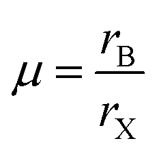
Stability, a critical physical parameter of perovskite materials, is a major factor restricting their commercialization. Specifically, polycrystalline perovskite thin films exhibit poor ambient stability and high sensitivity to moisture, oxygen, light and heat, which are attributed to the presence of grain boundaries. These grain boundaries are widely recognized as the initial sites of material decomposition: they contain a thin amorphous intergranular layer (more moisture-sensitive than crystalline regions), and their weak crystallinity causes rapid moisture-induced degradation along the boundaries. Additionally, they also act as channels for the thermally induced volatilization of organic iodides. Therefore, an increasing number of researchers are committed to improving the stability of polycrystalline perovskite thin film materials by increasing the formation energy, including the design of 2D perovskite structures and the introduction of additives. For example, Smith et al. reported that a device with parts of MA+ (CH3NH3+) replaced with PEA (C6H5CH2CH2NH3+) is more resistant to moisture and can be fabricated under humid conditions. Li et al. showed that alkylcarboxylic acid ω-ammonium additives as templates can improve the moisture stability of perovskite solar cells. Although tremendous efforts have been devoted to enhancing device stability by reducing grain boundaries and defects, current polycrystalline perovskite thin films still fall short of meeting the requirements for highly efficient devices with long-term stability. In comparison, single-crystal perovskites exhibit a perfectly long-range ordered ABX3 crystal structure with highly regular atomic arrangements, which nearly eliminates the grain boundaries, dislocations, voids, and other defects ubiquitous in polycrystalline counterparts. This low defect, grain-boundary-free architecture drastically diminishes reactive sites, impeding the inward diffusion and infiltration of erosive agents while suppressing the preferential cleavage of ionic bonds at defect loci, thereby endowing the material with significantly enhanced resistance to moisture and oxidation.69–74 Thus, the single-crystal perovskite materials not only maintain the basic physical parameters of polycrystalline counterparts but also exhibit superior stability owing to the absence of grain boundaries. Taking MAPbI3 as an example, Tao et al. proposed that the centimeter-sized CH3NH3PbI3 (MAPbI3) single crystal shows obvious excellent photoelectric performance and thermal stability compared to polycrystalline films. Meanwhile, Huang et al. observed that the MAPbI3 single crystals synthesized 2–3 years prior, when stored in an ambient atmosphere without any encapsulation, retained their black color and shiny crystal facets with no significant degradation (Fig. 2a and b). The MAPbI3 crystals exhibited relatively good thermal stability, as evidenced by thermogravimetric analysis. Specifically, the decomposition temperature of single-crystal samples (240 °C) is higher than those of their polycrystalline thin film counterparts (150 °C). Additionally, Dong et al. fabricated lateral-structure perovskite solar cells (PSCs) based on MAPbI3 single crystals by a simple MAI treatment procedure. The test results demonstrated that these devices exhibit excellent long-term operational stability, with no significant degradation observed after continuous operation for 200 hours (Fig. 2c). Subsequently, Yang et al. reported that a mass loss of the FAPbI3 single crystal occurred at 320–360 °C, which means the thermal stability of the MAPbI3 single crystal is lower than that of the FAPbI3 single crystal (Fig. 2d and e). Recently, (FAPbI3)0.9(MAPbBr3)0.05(CsPbBr3)0.05 single crystals with long-term stability against water–oxygen were prepared. This work provides a single-crystal-based paradigm for long-term stability studies from the perspective of the intrinsic structure.75–80
 |
| | Fig. 2 Stability of perovskite materials: (a) photographic images recorded the degradation process of MAPbI3 polycrystalline thin films at 85% humidity; (b) photograph of an MAPbI3 single crystal stored in air without encapsulation for more than two years.78 Copyright 2017, Royal Society of Chemistry. (c) Long term stability of the lateral-structure MAPbI3 single-crystal device.75 Copyright 2020, Springer Nature. (d and e) TGA–DSC curves and transformation of the phase structure of the FAPbI3 single crystal.79 Copyright 2016, Wiley-VCH. | |
2.2.2. Photoabsorption properties.
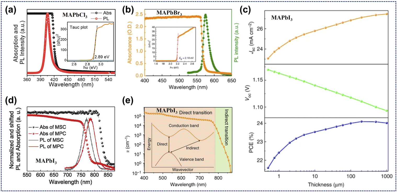
Compared with traditional semiconductors, perovskite semiconductors possess a higher optical absorption coefficient, which is very beneficial for diminishing the thickness of thin film materials employed in fabricating photoelectric devices. The approximately 500 nm thick polycrystalline thin films could achieve absorption in the entire visible spectrum. Distinct from polycrystalline thin films, single-crystal perovskites exhibit a broader light absorption range, stemming from their notable indirect-bandgap absorption. This unique absorption can be further explained by the distinct below-bandgap absorption in thick single-crystal materials (negligible in polycrystalline films). Moreover, the above-gap transition absorption coefficient is orders of magnitude higher than the below-bandgap counterpart This is largely due to the long-range ordered lattice of single crystals, which diminishes defects and non-radiative recombination, cuts absorption energy loss, and realizes superior absorption efficiency. As a typical example, previous studies on MAPbI3 have demonstrated that the energy of its indirect-bandgap absorption transition is 60 meV lower than that of the direct bandgap transition, and this difference accounts for its below-bandgap absorption.81–85 For example, the absorption onsets of MAPbCl3, MAPbBr3, and MAPbI3 single crystals are 430 nm, 570 nm, and 850 nm, respectively, whereas those of their thin film counterparts are approximately 407 nm, 550 nm, and 780 nm, respectively. This results in a long-wavelength shift of the absorption edge relative to the corresponding polycrystalline perovskite thin films. The photoluminescence peaks of these single crystals occur at wavelengths lower than their absorption onsets, which is attributed to the coexistence of direct and indirect band gaps.86–88 It has been reported that the shift of MAPbI3 single crystals is the major concern during these redshifts. This is attributed to two reasons primarily: one is the optical band gap of MAPbI3 (1.5 eV) being close to the bandgap of the optimal photovoltaic material, another is the increase of power conversion efficiencies in MAPbI3-based solar cells due to the upper limit of short-circuit current density caused by the redshift. Additionally, Huang et al. found that the carrier diffusion length of MAPbI3 single crystals was 175 ± 25 µm under 1 sun, which was suitable for the direct application of X-ray and gamma ray sensing.89–91 Liu et al. reported that the optical absorption of the MAPbI3 single crystal wafer can expand to 910 nm, which approximately shifted 110 nm compared to the thin film material (Fig. 3).92
 |
| | Fig. 3 Optical properties of single crystal perovskites: (a and b) light absorption and photoemission spectra of MAPbCl3 and MAPbBr3 single crystals.81,87 Copyright 2019, American Chemical Society. Copyright 2015, Springer Nature. (c) Calculated ideal dependence of PCE, JSC and VOC of single crystal solar cells on thin single-crystal thickness; (d) comparison of light absorption and photoemission spectra between MAPbI3 single crystal and its polycrystalline counterpart; (e) schematic of direct/below-bandgap transitions and absorption coefficient of polycrystalline MAPbI3 thin film.84,91 Copyright 2017, Springer Nature. Copyright 2015, The American Association for the Advancement of Science. | |
2.2.3. Carrier transport properties.
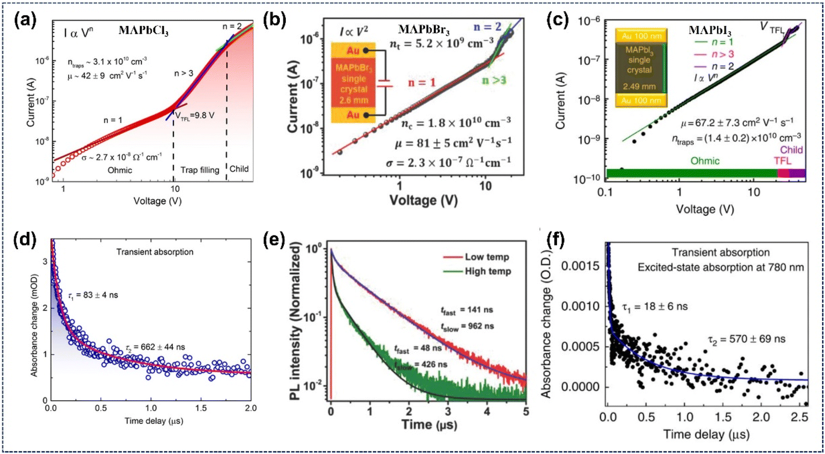
Electronic properties are among the important parameters for modeling photovoltaic and optoelectronic devices. Research shows that the high trap-state densities and defects in polycrystalline thin films provide recombination centers for charge carriers, thereby seriously decreasing their carrier lifetime and diffusion length. In contrast, bulk single crystals feature a tightly packed crystal structure, which minimizes grain boundaries and surface defects, and is conducive to enhancing the lifetime and diffusion length of charge carriers (Fig. 4). Additionally, the crystal symmetry of the ABX3 architecture in single-crystal perovskites governs carrier effective mass and migration paths. In high-symmetry lattices with well-ordered atomic configurations, migrating carriers experience negligible potential field fluctuations, translating to reduced effective mass and smooth transport. Meanwhile, varying degrees of lattice distortion alter carrier scattering patterns and migration channels, whereas the intrinsic low distortion characteristic of single crystals alleviates migration impediments and boosts transport efficiency. For instance, Beard et al. reported that the surface recombination velocity of MAPbBr3 single crystals was 3.4 ± 0.1 × 103 cm s−1, several orders in magnitude lower than that of important unpassivated semiconductors.93,94 Therefore, compared with polycrystalline thin films, single crystals with lower charge trap densities, higher carrier mobilities, longer diffusion lengths and carrier lifetime are better candidates for high performance optoelectronic applications. As shown in Table 1, Bakr et al. prepared MAPbX3 (X = Br, I) single crystals and found exceptionally low trap-state densities on the order of 109 to 1010, several orders in magnitude lower than that of their thin film counterparts.86,95 Huang et al. reported that bulk carrier diffusion length exceeded 175 µm under 1 sun illumination and even exceeded 3 µm under weak light, which outdistanced that of the polycrystalline thin films.91 Zhang et al. found that the diffusion lengths of MAPbI3−xClx (x = 0.005) exceeded 380 µm under 1 sun illumination, approximately two times higher than that of MAPbI3 single crystals.96 The difference in values given is mainly caused by different transport processes as revealed by measurement methods.
 |
| | Fig. 4 The carrier characteristics of single crystal perovskites: (a and b) transient absorption and I–V response of the MAPbCl3 single crystal; (c and d) I–V trace and a comparison of PL time-decay trace for MAPbBr3 single crystals; (e and f) I–V response and transient absorption of the MAPbI3 single crystal.54,81,122 Copyright 2015, American Chemical Society. Copyright 2018, Wiley-VCH. Copyright 2015, Springer Nature. | |
Table 1 Summary of single-crystal perovskite performance parameters
| Sample |
Trap density [1010 cm−3] |
Mobility [cm2 V−1 s−1] |
Carrier lifetime fast slow [ns] |
Technique |
Diffusion length [µm] |
Ref. |
| MAPbCl3 |
3.1 |
42 |
83 |
662 |
SCLC |
8.0–8.5 |
122
|
| MAPbCl3 |
0.79 |
64 |
— |
SCLC |
— |
87
|
| MAPbCl3 |
— |
179 |
— |
Hall |
— |
103
|
| MAPbBr3 |
2.6 (Hole) |
4.36 |
— |
Hall |
— |
103
|
| 11 (Electron) |
— |
| MAPbBr3 |
0.67 |
83.9 |
132 |
897 |
SCLC |
5.3–13.8 |
46
|
| MAPbBr3 |
0.62 |
81 |
139 |
899 |
SCLC |
5.4–14.2 |
54
|
| MAPbBr3 |
20 |
60 |
189 |
Hall |
5 |
95
|
| MAPbBr3 |
0.58 |
115 |
41 |
357 |
TOF |
3–17 |
86
|
| 20–60 |
Hall |
| 38 |
SCLC |
| MAPbBr3 |
0.65 (Electron) |
— |
997 |
SCLC |
— |
37
|
| 0.44 (Hole) |
| MAPbBr3 |
3 |
24 |
28 |
300 |
SCLC |
1.3–4.3 |
81
|
| MAPbI3 |
0.18 (Hole) |
34 |
— |
Hall |
— |
103
|
| 4.8 (Electron) |
| MAPbI3 |
3.3 |
2.5 |
22 |
1032 |
SCLC |
2–8 |
86
|
| MAPbI3 |
1.4 |
67.2 |
18 |
570 |
SCLC |
1.8–10.0 |
81
|
| MAPbI3 |
3.6 (Hole) |
164 ± 25 |
82 ± 5 µs (TPV) |
SCLC |
175 ± 25 |
91
|
| 34.5 (Electron) |
105 ± 35 |
95 ± 8 µs (IS) |
Hall |
| MAPbI3−xClx (x = 0.005) |
3.4 ± 1.5 |
70 |
489 ± 221 µs (IS) |
SCLC |
380 ± 40 |
96
|
2.2.4. Bandgap engineering.
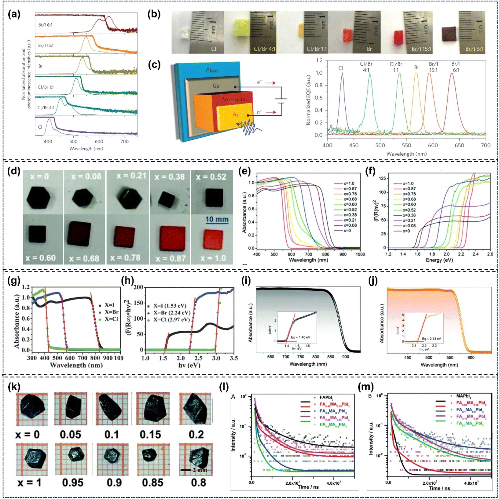
Spectral tunability stands as one of the most distinctive fundamental properties of perovskite crystal materials. Research shows that organic–inorganic hybrid perovskites are highly suitable for photovoltaic applications, as their bandgap can be tuned to the 1.0–1.7 eV range by modifying the compositions of organic cations and inorganic anions. In other words, the ABX3 lattice structure of single-crystal perovskites exhibits exceptional tunability, enabling precise modulation of bond lengths and angles between X site halide ions and A/B-site cations through ion doping or component regulation. These geometric variations in bonding directly influence the electronic band structure, thereby allowing fine-tuned control over the bandgap width.97–99,106 Currently, there are usually two efficient ways of bandgap tuning, one is to change the type and number of halogen atoms in ABX3 perovskites. In 2015, Huang et al. reported that MAPbBr3−xClx and MAPbI3−xBrx mixed halide perovskite single crystals with continuous tuning in the visible range could be applied in the narrowband photodetection (Fig. 5a–c).100 Then, Liu et al. prepared MAPb(BrxI1−x)3 (x = 0–1) single-crystal perovskites and found that the absorption spectrum of samples could shift in the wavelength range from green to red by changing the Br content in the single crystals (Fig. 5d–f).101 Han et al. reported that the MAPbI3−xBrx (I/Br = 10:1 in the precursor) single crystals had a long carrier lifetime of up to 262 µs under 1 sun illumination, approximately two times longer than that of MAPbI3 single crystals.102 The other is to change the type and size of organic cations. As reports show, the bandgap values of MAPbCl3, MAPbBr3, and MAPbI3 single crystals are 2.97, 2.24, and 1.53 eV, respectively (Fig. 5g and h), and that of FAPbBr3 and FAPbI3 single crystals are 2.13 and 1.4 eV, respectively (Fig. 5i and j).103,104 In 2017, Zhou et al. synthesized a series of FA(1−x)MAxPbI3 (x = 0–0.2, 0.8–1) single crystals and found that the carrier lifetime of FA(1−x)MAxPbI3 (x = 0.8–0.95) was longer than that of MAPbI3 (Fig. 5k–m).105 In addition, theoretical calculations show that the change of divalent cation is also responsible for the reduction of the bandgap.106
 |
| | Fig. 5 Properties of hybrid halide perovskite single crystal materials: (a–c) photographs, corresponding bandgap, absorption and photoluminescence spectra of MAPbBr3−xClx and MAPbI3−xBrx mixed halide perovskite single crystals.100 Copyright 2015, Springer Nature. (d–f) Photographs, Vis-NIR absorption spectrum and bandgap of MAPb(BrxI1−x)3 (x = 0–1) single-crystal perovskites.101 Copyright 2016, Royal Society of Chemistry. (g and h) UV-vis-NIR absorption spectrum and bandgap of MAPbX3 (X = Cl, Br, I) single crystals.103 Copyright 2015, Wiley-VCH. (i and j) Absorption spectrum and Tauc plots of FAPbX3 (X = Br, I) single crystals.104 Copyright 2015, Royal Society of Chemistry. (k–m) Photographs and time-resolved photoluminescence spectra of FA(1−x)MAxPbI3 (top: x = 0–0.2, bottom: x = 1–0.8) single crystals.105 Copyright 2017, Royal Society of Chemistry. | |
2.2.5. Low ion migration and defect density.
Electronic trap states play a pivotal role in the performance aging of perovskite optoelectronic devices, such as solar cells. In single-crystalline perovskite-based optoelectronic devices, these electronic trap states are primarily derived from bulk defects and surface defects within the material.5 Bulk defects predominantly arise during the growth of single crystals via low-temperature solution-based methods. Specifically, excessive temperature-dependent variations in the precursor solution concentration leads to uneven growth rates of the crystal across different time periods and crystal planes, thereby forming point defects such as Pb vacancies and I vacancies, which ultimately increase the bulk defect density.107,108 Surface defects are mainly caused by the erosion of the single crystal surface by solvents. Upon retrieval of the crystal from the growth solution, temperature fluctuations perturb the dissolution equilibrium (MAI > PbI2 in solubility). This perturbation triggers an imbalance in the surface composition, thereby inducing the formation of surface defects, leading to MA vacancies and Pb-enriched surfaces.84,91
To effectively suppress bulk defects in single crystals, the key is to scientifically and rationally regulate the crystal growth environment. Employing a slow heating or cooling method to reduce temperature change rate, which can mitigate fluctuations in the low-temperature crystallization environment and slow crystal growth, significantly minimizes the formation of various defects. For example, Liu et al. prepared high-quality MAPbBr3 single crystals via slow low-temperature gradient crystallization (25–60 °C). Compared with crystals grown at high temperatures (100 °C), the bulk defect density of these crystals decreased by approximately one order of magnitude, enabling the fabrication of high-performance photodetectors.54 Subsequently, they further employed a dynamic flow microreactor system for the growth of ultrathin single-crystal wafers with controllable properties. Results showed that the external circulation continuously supplied precursor solution for crystal growth, maintained uniform solution concentration and a stable growth environment, and yielded MAPbI3 single crystals with high crystallinity and low trap density (6 × 810 cm−3).48 Despite progress in controlling bulk defects, surface defects remain unavoidable due to solvent damage when crystals are retrieved from the solution. Reports indicate that the defect density near the crystal surface is several orders of magnitude higher than that in the bulk. Huang et al. observed distinct interfaces between two crystal layers by inducing discontinuous single crystal growth, and found significantly increased defect density at these interfaces, confirming that crystal surfaces contain more defects than the bulk.109 Surface defects in single crystals are typically passivated through chemical modification, physical coating, elemental doping, and interface engineering approaches. Huang et al. achieved a high-performance single-crystalline perovskite solar cell by coating a layer of MAI on the surface of MAPbI3 single crystals, with a PCE of up to 17.8%.84 Meantime, Bakr et al. reduced the growth temperature of single crystals using a mixed solvent, significantly suppressing the thermal decomposition of MAI on the MAPbI3 surface and achieving a PCE of 21.9% for single-crystalline perovskite solar cells.110
Perovskites, a class of ionic crystals with a soft lattice structure, undergo ion migration under external stimuli. When an electric field is applied to the perovskite layer, it not only enables hole/electron transport but also triggers the redistribution of mobile ions and defects (e.g., vacancies, interstitial ions).111,112 While perovskite ion migration involves both anions (e.g., I−, Br−) and cations (e.g., MA+, Pb2+), experimental and theoretical studies consistently confirm that in lead-based perovskites, iodide ions dominate the overall migration process due to their substantially lower migration activation energy and higher diffusion coefficient than other mobile ions. Ion migration imposes critical challenges to device performance: it alters the internal electric field distribution of the device, complicating the accuracy of device characterization. More importantly, it directly induces the photocurrent hysteresis effect, and accelerates both the decomposition of perovskite materials and the degradation of device performance.113,114 Studies on switchable photovoltaic effects conducted by Huang et al. have provided key insights into this phenomenon. Their research revealed that ion migration in polycrystalline perovskite films is likely dominated by grain boundaries. The conclusion arrived at was that devices based on large-grain films exhibit significantly higher switching difficulty compared to those with small-grain films.115 Additionally, they observed Br− diffusion (from PbBr2) in MAPbI3 polycrystalline films, whereas no such diffusion was detected in MAPbI3 single crystals (Fig. 6a–c). This result further confirms that grain boundaries serve as fast channels for ion migration.116 In contrast to polycrystalline films with dense grain boundaries, single-crystal perovskites have a long-range ordered, low-defect lattice with well-regulated atomic coordination. This intrinsic structural advantage not only eradicates the primary pathways for ion migration but also elevates vacancy formation energy, thereby achieving remarkable suppression of ion migration. Additionally, B site cations in single crystals form stable octahedral coordination with X site halides, anchoring halide ions and reducing their tendency to escape the lattice. Consequently, this not only ensures the stable performance of fabricated devices but also alleviates ion migration induced damage to perovskite materials.59,82
 |
| | Fig. 6 EDS study on Br− diffusion in MAPbI3: (a) SEM and EDX Br-element distribution images of a PbBr2 particle (without/with illumination); (b and c) Br-element line scans of MAPbI3 polycrystalline film and single crystal (without/with illumination).116 Copyright 2016, Royal Society of Chemistry. | |
3. Single crystal growth methods
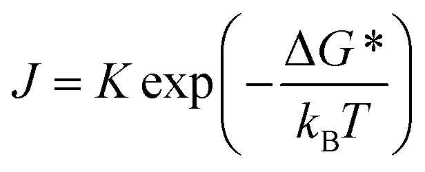
The properties of materials largely depend on their preparation methods. The performance of single-crystal materials is closely associated with their crystal quality, with higher quality yielding superior performance.117 Therefore, understanding the nucleation and growth mechanisms is crucial for developing more high-quality single-crystal perovskites. Similar to the growth mechanisms of other single-crystal materials, perovskite crystallization typically involves nucleation and growth. The difference lies in that perovskite crystallization can occur in solution, vapor, or molten systems. Generally, nucleation can be categorized into homogeneous nucleation and heterogeneous nucleation. Homogeneous nucleation refers to the spontaneous nucleation process without preferential nucleation sites, featuring the uniform formation of crystal nuclei in the mother liquor. That is to say, it occurs when components across the entire mother phase nucleate to generate a stable second phase without being influenced by impurities or external surfaces, and it is considered a thermodynamic process in nature.25,81 According to the classical nucleation theory, the nucleation rate (J) follows the Arrhenius-type equation below:19| | 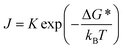 | (3) |
where K is a constant related to supersaturation concentration, ΔG* represents the nucleation barrier or Gibbs free energy change in nucleation, kB is the Boltzmann constant, and T stands for thermodynamic temperature. In contrast, heterogeneous nucleation is more prone to take place at preferential nucleation sites including phase interfaces, surfaces, or impurities, as stable nucleation surfaces are provided there. The selection of the nucleation process is determined by the requirements of different application fields, and the desired crystal size can be controlled accordingly.
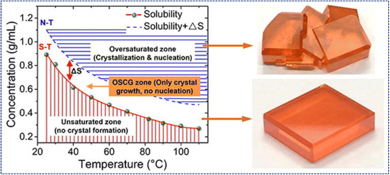
Fig. 7 shows the solubility curves corresponding to typical solution-based crystal growth methods, including inverse temperature crystallization, antisolvent crystallization, and volatile solvent crystallization. The horizontal axis stands for the crystal growth driving force (temperature variation), and the vertical axis for solution concentration. The crystallization process of perovskite crystals can be delineated by the solubility curve (S–T curve) and the nucleation curve (N–T curve) of the perovskite solution.46 Changes in the driving force trigger the system to transition among three distinct regions: the dissolution zone (crystal dissolution), the growth zone (steady crystal growth), and the nucleation zone (rapid crystallization). Since crystal growth requires a saturated growth solution, no crystallization or crystal growth takes place in the region below the S–T curve due to the unsaturated state of the perovskite precursor solution. Once the solution temperature surpasses the threshold defined by the S–T curve, the growth solution becomes saturated, allowing perovskite crystals to grow. As the temperature rises further, the solution moves into the supersaturation region above the N–T curve, where continuous energy supply surmounts the nucleation energy barrier and triggers crystal nucleation in the solution. However, the high energy level in this region tends to induce defects and twins in perovskite crystals, which renders it unsuitable for the sustained growth of single-crystal perovskites. Stringent regulation of crystal growth driving forces (temperature, solute concentration, and solution volume) is critical to avoiding adverse effects like crystal dissolution and unintended nucleation, which tend to cause grain boundaries and core stacking in the final crystalline products. Tiny driving force fluctuations can push the system out of the optimal growth region, particularly for narrow growth zone materials. For example, the 0.005 M solubility and super-solubility difference of inverse temperature crystallization grown FAPbBr3 crystals demands stringent temperature and concentration regulation.11 In addition, the growth rate of single-crystal perovskites is closely correlated with the temperature of the growth solution. Given the inherent limitations of solute transport in the growth solution, an excessively high growth rate is also detrimental to the preparation of high-quality single-crystal perovskites.
 |
| | Fig. 7 Solubility curves of different regions in the single-crystal growth model, concentration–growth temperature relationship, and photos of MAPbBr3 single crystal samples from distinct growth regions.46 Copyright 2019, Elsevier. | |
The kinetics of nucleation and growth are intricately governed by factors such as the degree of supersaturation, temperature, and the surface free energy of the substrate, all of which play pivotal roles in determining the final morphology and quality of the perovskite crystals. Extensive efforts have been devoted to the fabrication of high-quality single-crystal perovskites via the optimization of growth solution parameters. Depending on the morphology of the obtained single-crystal perovskite materials, these crystal growth techniques can be broadly classified into three categories: bulk crystal techniques, thin crystal techniques, and single crystal nanostructure techniques.118–140 In this section, bulk crystal techniques are introduced emphatically.
3.1. Growth of bulk single crystals
3.1.1. Solution temperature lowering (STL) method.
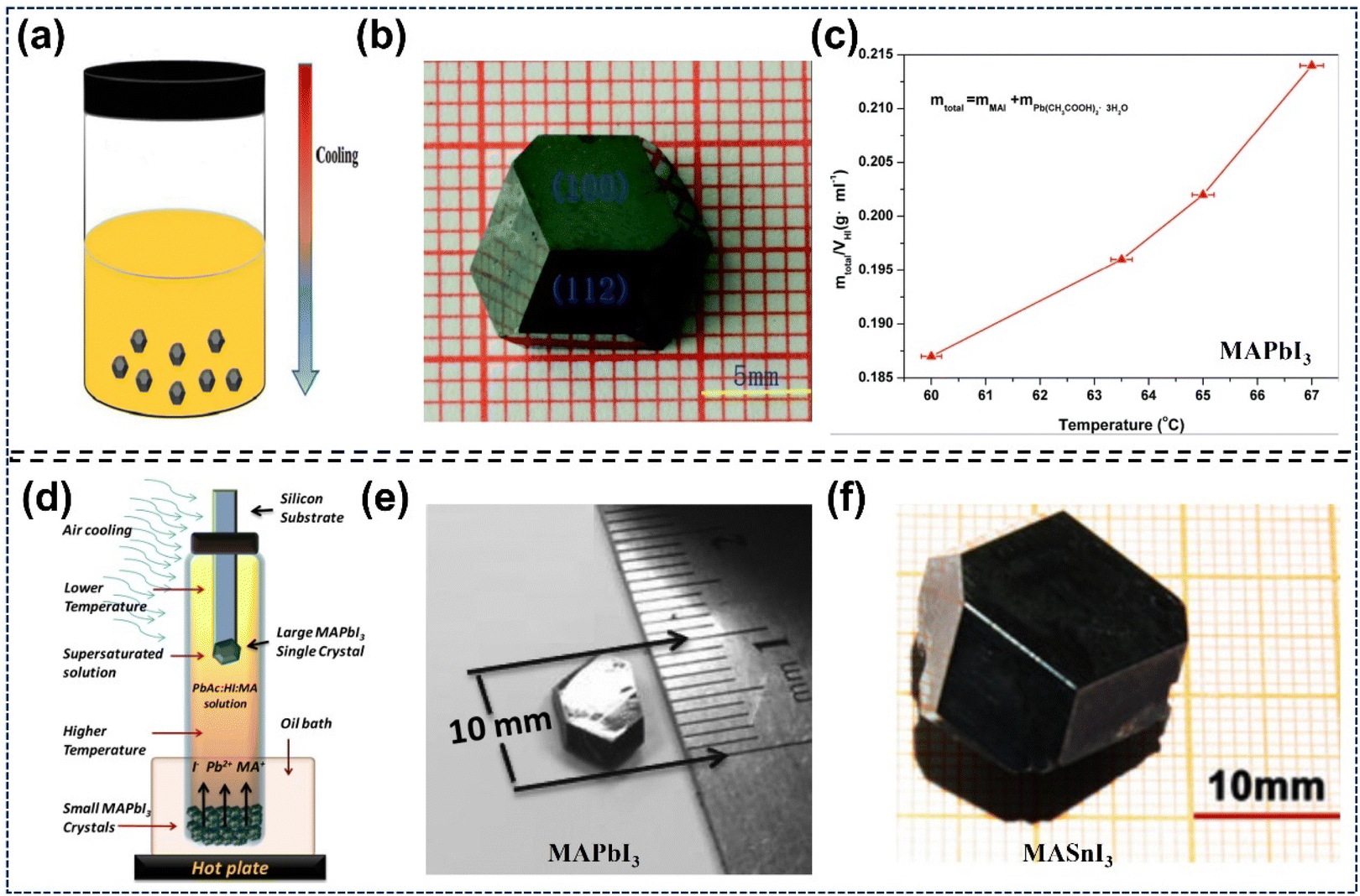
In 1987, Poglitsch and Weber pioneered the synthesis of CH3NH3PbX3 (X = Cl, Br, I) perovskite crystals via controlled cooling of concentrated aqueous HX acid solutions from elevated temperatures (∼100 °C) to ambient conditions.118 However, this initial approach predominantly yielded small-sized crystals, necessitating subsequent methodological refinements to achieve larger crystal dimensions. The STL method, a refined adaptation of Weber's pioneering technique, is a classic method for fabricating large-sized single-crystal perovskite materials. This method operates on the principle that perovskite solubility diminishes progressively as the temperature of a hot saturated solution decreases, triggering crystal precipitation upon reaching supersaturation. Specifically, large-sized single-crystal perovskites can be obtained by gradually cooling a precursor solution containing preformed seed crystals until supersaturation. Depending on the different fixed positions of the seed crystal, the crystal growth techniques are divided into top-seeded solution growth (TSSG) and bottom-seeded solution growth (BSSG). As a typical example, Tao's group obtained MAPbI3 single crystals with dimensions of 10 mm × 10 mm × 8 mm by using a BSSG method. The crystal growths were performed in a thermostatically controlled water bath using hydroiodic acid (HI) as the solvent, with the solution saturated at 65 °C. MAPbI3 seed crystals were preheated to 70 °C for 24 h to ensure complete dissolution. Bulk single crystals of MAPbI3 were grown over approximately one month by cooling the solution from 65 °C to 40 °C to induce saturation (Fig. 8a–c).76 In the same year, Huang's group reported the successful growth of large-size MAPbI3 single crystals (≈10 mm) via the TSSG method. The process involves three key steps: first, cooling the mixed solution to 75 °C and maintaining this temperature for one day to induce the precipitation of seed crystals; second, transferring these seed crystals to a container with a piece of silicon substrate; and finally, leveraging convective effects within the chamber to accelerate the nucleation of seed crystals on the silicon substrate, thereby facilitating the formation of large-sized crystals (Fig. 8d and e).91 Subsequently, Lian et al. prepared centimeter-sized MAPbI3 bulk single crystals using the BSSG method.119 Yan et al. obtained bulk single crystals with dimensions of 20 mm × 18 mm × 6 mm via a rapid solution temperature-lowering method.99 Recently, Tao's group synthesized bulk MASnI3 and FASnI3 single crystals through the TSSG method (Fig. 8f).120 Additionally, Ma et al. fabricated carbon-based CsPbI2Br perovskite solar cells using the TSSG method, achieving a PCE exceeding 14% while significantly enhancing device stability. This method effectively reduces film defects and improves crystallization quality.121
 |
| | Fig. 8 The STL method to prepare single-crystal perovskite materials: (a and b) BSSG method and the images of single crystals obtained by this method.76 Copyright 2015, Royal Society of Chemistry. (c) Solubility curve of MAPbI3 in HI solution.91 Copyright 2015, The American Association for the Advancement of Science. (d–f) Schematic illustration of the TSSG method and the single crystals prepared by this method.120 Copyright 2016, Wiley-VCH. | |
3.1.2. Inverse temperature crystallization (ITC) method.
Similar to the aforementioned STL method, ITC is also based on the abnormal solubility behavior of solutes across varying temperatures. The key distinction lies in that, within specific organic solvents, the solubility of these solutes exhibits a decreasing trend as the temperature rises. Bakr's group was the first to employ this method to synthesize a series of bulk MAPbX3 (X = Cl, Br, I) and FAPbX3 (X = Br, I) single crystals (Fig. 9a and b). Utilizing ITC, size/morphology-controlled crystals with low trap density and favorable charge transport properties can be rapidly obtained in hot solutions. It is worth noting that owing to different combinations of perovskite precursors and organic solvents, the crystals precipitate in some organic solutions, and not in others. For example, γ-butyrolactone (GBL) is a suitable solvent for forming MAPbI3 crystals, while MAPbBr3 crystals are suitable for being formed in N,N-dimethylformamide (DMF) solutions. In addition, researchers uncovered the role of surface tension in the rapid synthesis of single-crystal perovskites by using the ITC method during the process of investigating its nucleation and growth mechanisms (Fig. 9c–g).81,122–124 Subsequently, Liu's group prepared inch scale crystals by using the combination of seed-induced and ITC method. First, a large number of ≈1–2 mm seed crystals were collected in the hot mixed solutions, which were kept at 100 °C for two days. Then, a larger crystal was obtained by placing the original seed in the precursor solution. Finally, inch scale single-crystal perovskites could be harvested by repeating the above growth step several times. It is worth noting that the speed of growth is related to the size of seed crystals (Fig. 9h–l).103 Owing to the slow growth rate of traditional solution crystallization processes, Tao et al. prepared a centimeter-sized MAPbI3 single crystal by utilizing N2 air flow to increase solvent evaporation in the inverse temperature crystallization process.125 To improve the optoelectronic properties of FAPbBr3, Zhang et al. prepared Cl-doped FAPbBr3 single-crystal perovskites using the ITC method. Among these, FAPbBr2.9Cl0.1 exhibited the longest carrier lifetime. Youn S. S. O et al. used the ITC method to prepare Bi-doped MAPbBr3 to explore the effect of Bi concentration on the single crystal performance.122
 |
| | Fig. 9 Inverse temperature crystallization for single-crystal perovskites: (a and b) schematic illustration of the ITC method.81 Copyright 2015, Springer Nature. (c–g) Temperature-dependent solubility of perovskite materials in certain organic solvents; (h–l) single crystals prepared by the ITC method.103,104,122 Copyright 2015, American Chemical Society. Copyright 2015, Royal Society of Chemistry. Copyright 2015, Wiley-VCH. | |
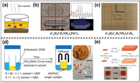
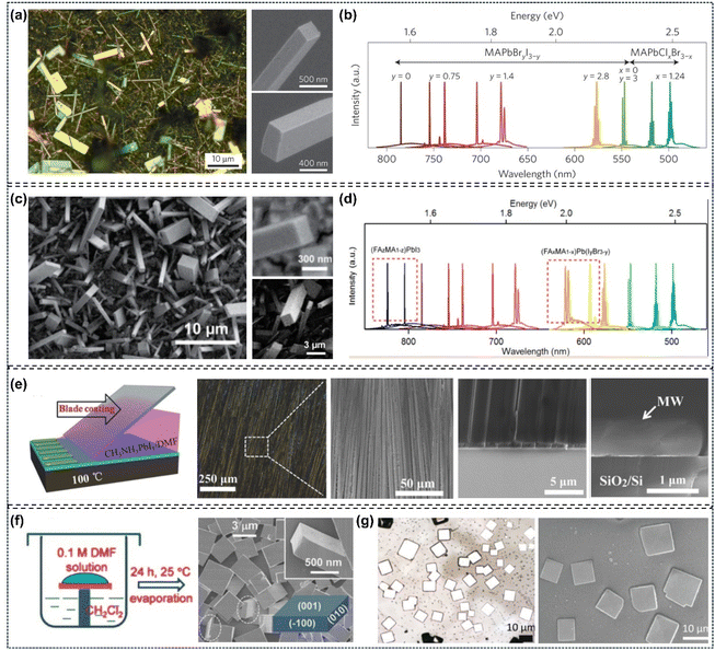
3.1.3. Slow evaporation (SE) method.
Compared with the STL and ITC methods, SE is a simpler and more convenient approach. It forms perovskite crystals via controlled solvent evaporation at a constant temperature (Fig. 10a).126 In 1997, Jakubas et al. adopted SE to prepare [NH2(CH3)2]GaCl4 (DMACG) single crystals.127 Liao et al. obtained bulk (C6H5CH2NH3)2PbCl4 single crystals with dimensions of 5 mm × 10 mm × 2 mm via slow evaporation. First, small crystals were synthesized from a concentrated aqueous HCl solution containing PbCl2 and benzylammonium chloride in the required stoichiometric ratio. Then, large crystals were harvested by controlled evaporation of the DMF solution at 363 K (Fig. 10b).128 For instance, Huang et al. prepared colorless (C6H5C2H4NH3)2CdI4 crystals at room temperature via slow solvent evaporation of a mixed solution, containing menthol, CdI2 and pre-synthesized C6H5C2H4NH3I (Fig. 10c).129 The SE method, easy to operate but with unsatisfactory performance, is not optimal for preparing large-sized, high-quality single crystals.
 |
| | Fig. 10 SE and AVC methods for single-crystal perovskite preparation: (a–c) SE method schematics and resultant crystals.128,129 Copyright 2015, Springer Nature. Copyright 2017, Royal Society of Chemistry. (d) AVC method schematics and harvested crystals.86 Copyright 2015, The American Association for the Advancement of Science. (e) Photographs of MAPbBr3 single crystals with different molar ratios.16 Copyright 2016, Springer Nature. | |
3.1.4. Anti-solvent vapor-assisted crystallization (AVC) method.
In contrast to the aforementioned methods, the AVC method is temperature-independent and solely relies on the selected solvent. This is primarily attributed to the solvent-dependent solubility variations of perovskites.12,25–27 As reported, perovskites display high solubility in GBL, DMF, and DMSO, but poor solubility in anti-solvents such as methylene chloride (DCM), acetonitrile (CAN), and chlorobenzene (CB).16,86 For instance, the groups of Cheng and Seok employed the AVC method to improve the flatness and uniformity of thin-film photovoltaics.130,131 Similarly, Bakr's group successfully obtained high-quality MAPbX3 (X = Br, I) single crystals using this method, in which an appropriate anti-solvent was slowly and evenly diffused into the precursor solution to reduce the solubility of the perovskite, ultimately leading to the formation of bulk crystals. The process involved two key steps: first, the precursor solution was prepared by mixing MAX and PbX2 (X = Br, I) in DMF or GBA; second, the container containing the precursor solution and DCM or GBA solvent was sealed, allowing DCM or GBA vapor to diffuse slowly into the precursor solution. As the diffusion proceeded, the concentration of the perovskite increased gradually, leading to the precipitation of bulk crystals from the solution. Specifically, they synthesized MAPbBr3 crystals using a 1:1 molar ratio of MABr and PbBr2 (Fig. 10d).86 However, Huang's group demonstrated that a 0.8 molar ratio of MABr to PbBr2 is more favorable for growing high-quality MAPbBr3 crystals, which arises from the significant solubility difference between the two components (Fig. 10e).16 Additionally, other perovskites including CsPbBr3 and Cs4PbBr6 crystals were also synthesized successfully by the AVC method.43,44
3.2. Growth of thin single crystals
Bulk single-crystal perovskites grown in three dimensional spaces exhibit high light absorption loss due to their large thickness, rendering them unsuitable for direct application in vertical-type optoelectronic devices. However, this structure is actually superior to planar-type optoelectronic devices. Consequently, there is an urgent need for single-crystal perovskite wafers to develop high performance optoelectronic devices.37,38,132,133
3.2.1. Chemical vapor deposition method (CVD).
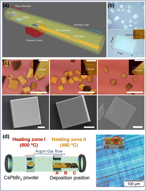
While high quality single-crystal perovskites have been obtained via wet-chemical methods, the solvents, surfactants, and other unintended impurities introduced during the solution-phase synthesis process will compromise the purity and overall quality of the final materials. As a solvent-free fabrication technique, CVD demonstrates exceptional performance in regulating thin film morphology, minimizing surface defects, and improving material quality and stability. As shown in Fig. 11a, CVD growth involves a tube with the carrier gas inlet on the left and a vacuum-pumped exhaust port on the right. The gas flow transports precursors to the substrate for sequential reactions, deposition and crystallization. Shi et al. adopted this configuration to obtain ultrathin (sub-10 nm) and large scale (a few tens of micrometers in lateral dimension) single crystalline 2D perovskite thin films on layered muscovite mica. Ordered perovskite films were successfully obtained, yet significant lattice mismatch and entirely disparate lattice types were observed between the substrate and the target material (Fig. 11b).134 Duan et al. demonstrated the one-step CVD growth of CsPbX3 (X = Cl, Br, I) microplatelets on diverse substrates (Si/SiO2 wafers, reduced graphene oxide, graphene, and 2D MoS2). All CsPbX3 microplatelets show intense, tunable PL covering blue, green and red bands. Particularly, CsPbBr3 microplatelets serve as dual gain media and WGM cavities to enable room-temperature lasing, while graphene/CsPbBr3/graphene heterostructures can fabricate vertical photodetectors with high photocurrent gain (Fig. 11c).135 In 2021, Nie et al. successfully fabricated high-quality and large-area CsPbBr3 SCTFs with millimeter-scale crystalline grains. This was accomplished by systematically varying substrate types and positions to precisely control the deposition rate and growth temperature, resulting in a maximum lateral grain size exceeding 3.1 mm (Fig. 11d).136 Although CVD is applicable for large-scale thin-film fabrication, both single-source (CsPbBr3) and dual-source (CsBr, PbBr2) deposition strategies for CsPbBr3 present prominent challenges. For the former, unvalidated congruent evaporation causes Cs/Pb-enriched films with low phase purity. For the latter, surface kinetics disturb component concentrations, rendering it prone to forming impurity phases during CsPbBr3 deposition. As per these considerations, Li et al. investigated single-/dual-source deposition for phase-pure CsPbBr3. By analyzing evaporation products via Knudsen Effusion Mass Spectrometry and growth products at varied temperatures, they found that CsPbBr3 decomposes partially congruently with precursor composition shifts; raising the temperature mitigates this by desorbing excess PbBr2. Dual-source evaporation yields high-purity CsPbBr3 at elevated temperatures (CsBr-limited growth), while lower temperatures lead to impurity phases (CsPb2Br5, Cs4PbBr6).137
 |
| | Fig. 11 CVD method for single-crystal perovskite preparation: (a and b) schematic illustration and film morphology of the CVD synthesis of MAPbCl3.134 Copyright 2015, Royal Society of Chemistry. (c) Photographs and AFM images of CsPbX3 (X = Cl, Br, I) microplatelets.135 Copyright 2017, Springer Nature. (d) Schematic of the CVD setup with variable substrate positions and corresponding image of CsPbBr3 single crystal thin films prepared via the CVD method.136 Copyright 2021, Wiley-VCH. | |
3.2.2. Bridgman method.
The Bridgman method, a conventional yet reliable crystal growth technique for melt-grown crystals, relies on precisely tailored temperature gradients and controlled solidification to produce large, high-quality crystals with negligible defect density. Fig. 12a is the three-dimensional diagram of a typical Bridgman furnace. Divided into four stages (raw material melting, gradient regulation, crystal growth, extraction and processing), the Bridgman growth process achieves high-quality single crystals by precise temperature control and slow crucible movement to establish stable gradients, enabling bottom-to-top crystallization followed by cooling, extraction, cutting and polishing.138 Kanatzidis and co-workers pioneered CsPbBr3 synthesis by the vertical Bridgman method, obtaining 7 mm diameter crystal ingots via a three-zone furnace at 10.0 mm h−1 translation speed under a set temperature profile, as shown in Fig. 12b.139 As shown in Fig. 12c, Tao et al. prepared high-quality large-sized CsPbBr3 single crystals via repeated directional crystallization and impurity removal, improving carrier transport properties. By means of the X-ray orientation technique, they carried out the first-ever exploration of the material's anisotropic optoelectronic properties, uncovering distinct variations in optoelectronic performance across various crystal planes. This threefold enhancement in responsivity and EQE of the optimal plane stems from the modulation of carrier transport enabled by the material's structural anisotropy.140 Large-size CsPbCl3 single crystals were synthesized via the Bridgman method, as illustrated in Fig. 12d. The resultant crystals are pale-yellow and feature high optical transparency, with transmittance exceeding 80% across a broad wavelength range. Such high optical transparency is indicative of low impurity content in the CsPbCl3 single crystals.141 Furthermore, Zhang et al. obtained centimeter-sized bulk single crystals of CsPbBr3−3nX3n using a modified Bridgman technique. Specifically, polycrystalline precursors were first synthesized, followed by heating at a temperature ranging from 550 to 650 °C for 6 h in a homemade vertical furnace equipped with dual temperature zones. The precursors were then slowly transferred to the low-temperature zone to induce crystallization, after which the system was cooled to room temperature at a controlled rate of 5–15 °C h−1. The as-grown crystals exhibited high structural stability and tunable optoelectronic properties, and were subsequently processed via cutting to obtain samples with dimensions of 7 mm × 7 mm × 1.5 mm (Fig. 12e).138 Although the Bridgman method enables the production of large-size crystals in sealed ampoules, the interfaces between the crystal and the ampoule may induce internal stress, fissures or microscopic grain boundaries within the crystals. Moreover, it is only suitable for organic–inorganic compounds with established melting points, as organic substances exhibit high vapor pressure and poor chemical stability at melting temperatures.
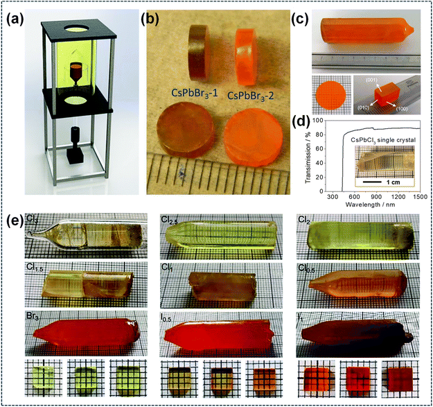 |
| | Fig. 12 Bridgman method for single-crystal perovskite preparation: (a) diagram of the homemade Bridgman furnace.138 Copyright 2021, Royal Society of Chemistry. (b) Photograph of the single-crystal specimens of CsPbBr3.139 Copyright 2013, American Chemical Society. (c) Photographs of the as-grown CsPbBr3 single crystal (upper), polished wafer (lower left), and oriented cuboid CsPbBr3 single crystal (lower right).140 Copyright 2018, American Chemical Society. (d) Optical transmission of CsPbCl3 single crystals. Inset: Bridgman-grown CsPbCl3 ingot.141 Copyright 2021, American Chemical Society. (e) Photographs of the as-grown CsPbBr3−3nX3n bulk crystals.138 Copyright 2021, Royal Society of Chemistry. | |
3.2.3. Other types of growth methods for thin single-crystal materials.
Currently, the growth technology of single-crystal perovskite wafers has become a research hotspot, as it is suitable for improving device performance. Liu's group sliced the as-prepared large FAPbI3 crystals into thin wafers (≈100 µm) using a diamond wire sawing machine. As shown in Fig. 13a, the large FAPbI3 crystals were mounted on the sample holder of the slicing machine, and moved slowly toward the revolving wire at a specific speed. By controlling the sawing speed and crystal feeding rate, perovskite wafers with well-defined shapes and sizes could be obtained.38 Subsequently, Bakr's group fabricated high-quality MAPbBr3 single-crystal perovskites (≈150 µm) via mechanical polishing.142 Yan's group obtained MAPbI3 perovskite single-crystal thin films (≈15 µm) by treating the cut and polished samples using a chemical etching technique (Fig. 13b). The sliced and polished wafers (≈200 µm thick) were immersed in an etching solution, which was the residual mother liquor from bulk crystal growth. By controlling the immersion time, etching solution concentration and temperature, the desired wafer thickness could be achieved.47
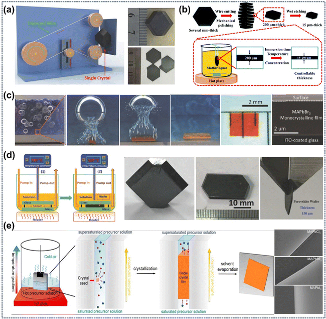 |
| | Fig. 13 Fabrication of single-crystal perovskite wafers and growth mechanism of their thin crystals: (a) schematic of diamond wire sawing machine and sliced FAPbI3 wafers.38 Copyright 2016, Wiley-VCH. (b) MAPbI3 single-crystal film fabrication process.47 Copyright 2018, Royal Society of Chemistry. (c) Microscopic CTAC mechanism schematic and resulting monocrystalline film.82 Copyright 2016, Wiley-VCH. (d) Ultrathin single-crystal wafer preparation schematic and microreactor-grown wafers.48 Copyright 2016, Wiley-VCH. (e) Space-limited technique schematic for on-substrate growth of large-area, thickness tunable single-crystalline perovskite thin films.36 Copyright 2016, American Chemical Society. | |
Apart from these methods, the cavitation-triggered asymmetrical crystallization (CTAC) method and space-limited technique have also gained favor among researchers. In 2016, Bakr's group obtained homogeneous MAPbBr3 perovskite single-crystal thin films with thickness ranging from 1 to 60 µm using the CTAC method assisted by ultrasound. Fig. 13c illustrates the entire CTAC process. Owing to the successive cyclic compression and rarefaction of ultrasound waves, cavities are created and collapsed, releasing ultrahigh energy that can induce nucleation. This energy can typically overcome the nucleation barrier formed by rapid cooling in local zones, increased local pressure, and energy accumulation. Additionally, the growth of asymmetric crystals is related to the collapse of cavities, which is typically asymmetric near the solid surface, and their high-speed fluid can jet toward the substrate.82 Liu's group successfully prepared a series of ≈150 µm thin wafers using the space-limited technique in a dynamic flow microreactor system (Fig. 13d). The gap between the two thin glass slides plays a crucial role in determining the thickness of the resulting samples.48 Subsequently, the Kuang and Huang groups adopted a similar technique to grow thin perovskite single-crystalline wafers of approximately 10 µm.35,84 Hu's group reported a facile space-confined solution-processed strategy to on-substrate grow various hybrid perovskite single-crystalline thin films in the size of submillimeter with adjustable thicknesses from nano- to micrometers. As illustrated in Fig. 13e, two clean flat substrates were clipped together and then vertically dipped in perovskite precursor solution. Capillary pressure enabled the solution to spread over the entire substrates, while the thickness of perovskite single-crystalline thin films was well-defined by the inter-substrate gap, which can be easily tuned by the clipping force.36 Notably, Ma's group optimized the thickness of single-crystalline thin films down to hundreds of nanometers by improving the previous preparation method, which provides the possibility of obtaining large-area single-crystalline thin-films. Specifically, they improved the previously reported ITC technique in three aspects:
(1) Growing crystals between two face-to-face substrates with a micrometer-sized gap to disrupt isotropic growth.
(2) Controlling thickness via pressure applied to the gap.
(3) Conducting surface modification on substrates (hydrophobic treatment of silicon surface and oxygen plasma treatment of ITO surface).143
3.3. Growth of single crystal nanostructures
Owing to their size-dependent and excellent optoelectronic properties, single-crystalline perovskite nanostructures show exceptional promise for application in nanoscale optoelectronic and photonic devices, particularly in the realization of miniaturized lasers.39,42 Since the preparation methods of these materials play a vital role in improving device quality, numerous researchers have focused on the controlled synthesis of perovskite single-crystalline nanostructures.34,41,50 For example, Jin's group obtained single-crystalline CH3NH3PbX3 (X = Cl, Br, I) nanowires with a length of approximately 20 µm and flat rectangular end facets via a surface-initiated solution growth strategy. These nanowires were synthesized by immersing a Pb(CH3COO)2 thin film (deposited on a glass slide) in an isopropanol solution of MAX under ambient conditions at room temperature. They also observed room temperature lasing operations in most NWs with mixed stoichiometries, covering the emission range from the near-infrared to the visible region (Fig. 14a and b).15 Subsequently, they adopted the same method to harvest single-crystalline FAPbX3 (X = Br, I) nanowires, which exhibit better photostability and wider wavelength tunability than MA-based counterparts. Among them, both FAPbI3 and FAPbBr3 NWs demonstrated lasing behavior with low lasing thresholds (several microjoules per square centimeter) and high quality factors (1500–2300. In particular, FAPbI3 (and MABr-stabilized FAPbI3) NWs exhibited optically pumped room temperature near-infrared (∼820 nm) lasing, whereas FAPbBr3 showed green lasing. They further demonstrated tunable nanowire lasers operating across a broader wavelength range, which are based on FA-based lead halide perovskite alloys (FA, MA) PbI3 and (FA, MA) Pb (I, Br)3via cation and anion substitutions (Fig. 14c and d).17 Subsequently, Jie's group reported dragging a DMF solution of MAPbI3 across a hot (100 °C) substrate. After evaporation of the exposed solution front, MAPbI3 microwire arrays formed, which are primarily aligned along the blade movement direction and have lengths of up to 1 cm. The scanning electron microscopy images revealed that the as-synthesized samples were straight with uniform width ranging from 2 to 3 µm. The molecular layers feature a smooth top surface and homogeneous color variation across the entire region, indicating the single-crystal nature of the perovskite molecular layers. Further characterization of the smooth cross-sectional surface of the molecular layers also confirms their high crystallinity (Fig. 14e).144 Meanwhile, Zhu's group prepared patterned MAPbBr3 single-crystalline microplates on an FTO substrate via an Ostwald ripening assisted photolithography (ORAP) method.145 Fu's group obtained single-crystalline square MAPbBr3 microdisks with a thickness of approximately 500 nm through a one-step solution self-assembly process (Fig. 14f).146 Additionally, Xiong's group synthesized single-crystalline CH3NH3PbX3 (X = Br, I) and CH3NH3PbIxCl3−x nanowires using a two-step vapor phase method. First, PbX2 (X = Br, I) nanowires were prepared via the chemical vapor deposition (CVD) method in a quartz tube. Then, the target products were formed through gas–solid heterophase reactions between MAX molecules and PbX2 nanowires using the same CVD method.147 Wang's group achieved size-controlled single-crystalline CH3NH3PbBr3 microplatelets and microstrips by adjusting the concentration of the precursor solution, via a process involving slow diffusion and evaporation of DMF (Fig. 14g).148 Besides the widely studied single-crystalline organic lead halide perovskite nanostructures, some inorganic counterparts such as CsPbBr3 have also been successfully synthesized.23,33Table 2 summarizes the merits, limitations, application ranges, and specific effects on material performance of the various growth methods.
 |
| | Fig. 14 The structural characterization of single-crystal perovskite nanostructures: (a) optical and magnified SEM images (top view) of single crystal MAPbI3 perovskite nanowires; (b) widely tunable lasing emission wavelengths at room temperature from single-crystal NW lasers of mixed lead halide perovskites.15 Copyright 2015, Springer Nature. (c) SEM images of as-grown MABr-stabilized FAPbI3 perovskite nanowires; (d) broad wavelength-tunable lasing from FA0.67MA0.33PbBr2.69I0.31 NWs.17 Copyright 2016, American Chemical Society. (e) Schematic illustration, optical images, and SEM images of MAPbI3 microwire arrays.144 Copyright 2016, Wiley-VCH. (f) Low-magnification and high-magnification SEM images of single-crystalline square MAPbBr3 perovskite microdisks.146 Copyright 2015, Wiley-VCH. (g) Optical microscopic images and top-view SEM image of single-crystalline CH3NH3PbBr3 microplatelets.148 Copyright 2019, Wiley-VCH. | |
Table 2 Systematic comparative evaluation of various growth methods
| Growth method |
Advantages |
Disadvantages |
Application scope |
Impact on material performance |
| STL |
Convenient operation; low cost |
Materials/time consuming; nucleation control difficulty |
Lab-scale small-batch basic research |
High photoelectric conversion efficiency; stability restricted by interface defects |
| ITC |
Fast growth rate; simple operation |
Temperature sensitive; solvent limitation |
Preparation of single-crystal samples for preliminary performance testing |
High carrier mobility |
| SE |
Low cost; simple equipment |
Long growth cycle; small crystal size; high defect density |
Lab-scale small-batch basic research |
Medium carrier mobility; moderate stability |
| AVC |
Fast growth rate; energy saving |
Small crystal size; random growth |
Rapid preparation of single-crystal samples for preliminary performance testing |
High photoelectric conversion efficiency |
| Space-confined method |
Controllable thickness |
Small area; thickness control confined to the range of micrometer to tens of micrometers |
Suitable for growth of single-crystal films |
High interface defects |
| CVD |
Low cost; defect reduction; high reproducibility |
Precise parameter control required; temperature limitation |
Suitable for industrial production |
Consistent crystal orientation, significant carrier transport anisotropy |
| Bridgman method |
Temperature tunable; high quality; large crystal size |
Unsuitable for organic component growth |
Preparation of high-purity bulk single-crystals for basic physical property research |
Good crystal integrity, few deep-level defects, excellent stability |
4. Applications
By virtue of their excellent semiconductor performance, perovskite ABX3 materials have garnered substantial attention in diverse optoelectronic applications, including photodetectors, solar cells, light-emitting diodes, lasers, high-energy ray detectors and other fields.24 In this section, we focus on summarizing several representative applications.
4.1. Photodetectors
Photoelectric conversion technology is pivotal in key application areas such as optical communication, environmental monitoring, and digital-image sensing. As devices that convert optical signals into electrical ones, photodetectors stand as ideal candidates for the optoelectronic field.18 Studies indicate that single-crystal perovskite photodetectors exhibit superior stability and photoelectric performance compared to their polycrystalline counterparts.48,119,122,149 Typically, the key parameters characterizing photodetector performance include responsivity (R), detectivity (D*), external quantum efficiency (EQE), and response time (τ). Table 3 summarizes the key performance parameters for single-crystal perovskite photodetectors.
Table 3 Summary of detection performances of perovskite single-crystal photodetectors
| Sample |
Responsivity [A W−1] |
Detectivity [Jones] |
EQE [%] |
Rise time [10–90%] |
Decay time [90–10%] |
Ref. |
| MAPbCl3 |
0.046 |
1.2 × 10¹⁰ |
— |
24 ms |
62 ms |
122
|
| MAPbCl3 |
3.73 |
9.97 × 10¹¹ |
1115 |
130 ns |
368 µs |
87
|
| MAPbBr3 |
0.115 |
— |
3.17 |
2.3 s |
2.76 s |
150
|
| MAPbBr3 |
55.7 |
8 × 10¹³ |
13453 |
27.6 µs |
15.8 µs |
46
|
| MAPbBr3 |
4 × 10³ |
— |
1.5 × 10⁴ |
— |
25 µs |
95
|
| MAPbBr3 |
1.6 × 10⁷ |
1.3 × 10¹³ |
1.5 × 10⁷ |
81 µs |
892 µs |
143
|
| MAPbBr3 |
0.043 |
5.29 × 10¹⁰ |
— |
453 µs |
493 µs |
201
|
| MAPbBr3 |
7 |
4.2 × 10¹¹ |
— |
0.5 ms |
0.78 ms |
187
|
| MAPbI3 |
0.035 |
— |
100 |
139 µs |
227 µs |
47
|
| MAPbI3 |
4.95 |
2 × 10¹³ |
— |
<0.1 ms |
— |
19
|
| MAPb(BrxI1−x)3 (x = 0.78) |
2.36 |
2.01 × 10¹² |
639 |
3.4 ms |
3.6 ms |
101
|
| FAPbI3 |
4.5 |
— |
900 |
8.3 ms |
7.5 ms |
38
|
| (PEA)2Pb(I1−xBrx)4 |
4.8 |
6.5 × 10¹³ |
— |
— |
— |
198
|
| CsPbCl3 |
32.8 |
4.22 × 10¹² |
10867 |
200 µs |
420 µs |
199
|
| FAPbBr2.5I0.5 |
0.059 |
4.95 × 10¹⁰ |
34.51 |
202 µs |
331 µs |
200
|
| (FASnI3)0.1(MAPbI3)0.9 |
0.53 |
7.09 × 10¹⁰ |
82.5 |
22.78 µs |
20.35 µs |
8
|
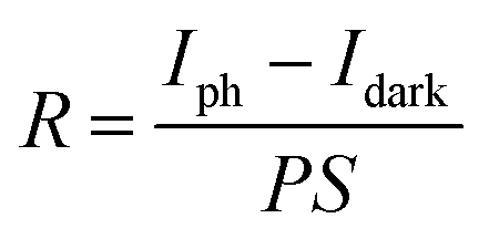
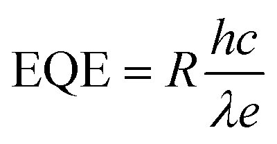
R is the ratio of photocurrent to incident light intensity, reflecting the efficiency of converting light into photocurrent, and can be calculated as follows:43
| |  | (4) |
where
S denotes the effective illuminated area,
P is the irradiance power density, and Δ
I is the current difference under illuminated (
Iph)
versus dark (
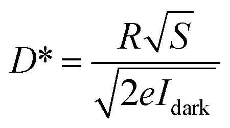
Idark) conditions. Given that a higher
D* value implies superior weak signal detection capability, this parameter serves as a critical metric for evaluating photodetector sensitivity and can be expressed as:
20,45| |  | (5) |
where
e is the elementary charge. EQE is an important parameter used to quantify the efficiency of photon to photocurrent conversion and can be determined as follows:
14,95| |  | (6) |
where
h is Planck's constant,
c is the speed of light, and
λ is the wavelength of incident light. Parameter
τ, the photoelectric conversion transit time of the photodetector, characterizes temporal response latency: the output electrical signal shows finite rise time to steady state under illumination and delayed decay when irradiation stops. Specifically,
τ is defined as the duration required for the photoresponse to rise from 10% to 90% of its initial value or fall from 90% to 10% of its maximum value.
28,37
As early as 2015, Lian et al. fabricated a high performance planar-type MAPbI3 single-crystal photodetector (MSCP) by depositing a pair of interdigitated Au-film electrodes on the MAPbI3 (100) facet (Fig. 15a). Under uniform illumination at 1 mW cm−2 irradiance, the MSCP exhibited an R value of 2.55 A W−1 and an EQE value of 5.95 × 10²%, while the MAPbI3 polycrystalline film photodetector (MPFP) showed significantly lower values of 0.0197 A W−1 and 4.59%, respectively. These results confirm that the MSCP achieves over two orders of magnitude enhancement in both R and EQE compared to the MPFP (Fig. 15b and c). Transient photocurrent response measurements showed that the MSCP has a rise time of 74 µs after triggering and a decay time of 58 µs after irradiation is terminated. Its response speed is three orders of magnitude faster than that of the MPFP (Fig. 15d).119 Subsequently, Ma's group fabricated an MAPbBr3 single-crystalline thin film (SCTF) photodetector with a thickness of 380 nm, and observed that optimizing the SCTF thickness could enhance both the lowest detectable power and internal gain by several orders of magnitude.143 Liu's group reported that they prepared approximately 100 photodetectors on a piece of MAPbI3 perovskite single-crystalline wafer, with the devices exhibiting a photocurrent about 350 times higher than that of comparable microcrystalline thin-film photodetectors (Fig. 15e–g).48 They also developed a Vis-NIR photodetector based on dual-halide single-crystal perovskites, identifying the optimal response spectra at a bromine content of 0.78.101 Additionally, Bakr's group exploited a photodetector based on MAPbCl3 single-crystal perovskites, which is applicable for ultraviolet detection.122 The single-crystal perovskite-based photodetectors fabricated by Huang's group realized a highly narrowband response with a full-width at half-maximum of <20 nm, attributed to the fast surface-charge recombination (Fig. 15h–j).100 Meanwhile, Lin et al. fabricated photodetectors based on MAPbBr3/MAPbI3 single-crystalline photodiodes and photoresistors, which enabled photoresponses to near infrared light through trap-related linear sub-gap absorption.29 Recently, Chang et al. employed low-temperature space-limited crystallization technology to prepare high-quality (FASnI3)0.1(MAPbI3)0.9 narrow-bandgap Sn–Pb mixed single-crystal perovskites, which were applied in high-performance near infrared photodetectors. The devices achieved an EQE of 82.5% with a response time of only 22.78 µs (Fig. 15k–m).8 Yadav et al. investigated facet-dependent photodetection in MAPbI3 single crystals, reporting ON/OFF ratios of ∼620 for the (112) facet and ∼410 for the (100) at a bias voltage of 10 V.10
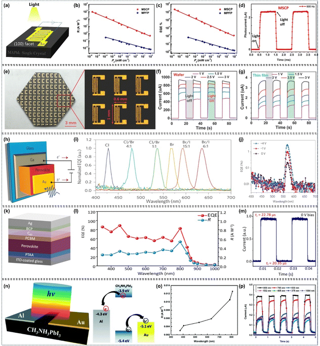 |
| | Fig. 15 Device structures and key performance parameters of single-crystalline perovskite photodetectors: (a–c) a planar-type MAPbI3 single crystal photodetector, along with a comparison of responsivity and EQE between the as-fabricated MSCP and MPFP; (d) transient photocurrent response of the MSCP.119 Copyright 2015, Springer Nature. (e–g) Photograph of approximately 100 photodetectors fabricated on an SC wafer, and a comparison of photocurrent response between the SC perovskite wafer and its SC thin film.48 Copyright 2016, Wiley-VCH. (h–j) Device structure for realizing highly narrowband response and ultra-narrow tunable EQE spectra.100 Copyright 2015, Springer Nature. (k–m) Structure and performance of multiple-layer device architecture with (FASnI3)0.1(MAPbI3)0.9 single crystal as the light absorption layer.8 Copyright 2016, Royal Society of Chemistry. (n–p) A single-crystalline perovskite-based photovoltaic photodetector and its photoresponse characteristics at different irradiance wavelengths.149 Copyright 2016, Royal Society of Chemistry. | |
At present, the majority of reported perovskite-based photodetectors are photoconductive types, which necessitate an external bias voltage for operation. Consequently, photovoltaic photodetectors have recently emerged as a promising alternative in the field, owing to their self-powered photodetector systems.13,142,149 As a typical example, the Yan group designed a self-powered photodetector based on perovskite MAPbI3 single crystals. The device operates via a built-in electric field generated by the Schottky junction between the Au and Al electrodes. It realized broadband detection across the wavelength range of 375 nm to 808 nm and demonstrates a responsivity of 0.24 AW−1 under an incident power density of 1 × 10⁻⁸ W cm−2 at 808 nm (Fig. 15n–p).149 Meanwhile, Huang's group designed an X-ray detector with a typical p–i–p structure, which is based on the perovskite MAPbBr3 single crystal.16 The Wei group constructed a self-power photodetector based on a perovskite MaPbBr3/MAPbIxBr3−x heterojunction single crystal. This device is driven by the built-in electric field within the junction and exhibits a responsivity of 11.5 mA W−1 at 450 nm under zero bias, which is an order of magnitude higher than that of its pure MAPbBr3 counterpart.150 In 2025, Xu et al. developed self-powered perovskite quantum dot photodetectors via Cr3+ doping and MXene interfacial engineering. These devices exhibit a high responsivity of 186.9 mA W−1 and a detectivity of 1.85 × 1012 cm Hz1/2 W−1, showing strong potential for chlorophyll-a concentration monitoring based on the Beer–Lambert law. This study provides a novel approach for developing high-performance self-powered photodetectors and advancing water pollution monitoring.9
4.2. Solar cells
In recent years, PSCs have made remarkable strides in terms of PCE. This impressive progress is primarily attributed to the exceptional properties of semiconductor perovskite materials, which include high carrier mobilities, high optical absorption coefficients, long carrier diffusion lengths, and suitable band gaps for photovoltaic devices.40,51,52,151 However, two significant challenges continue to impede the commercialization of PSCs: hysteresis effects and environmental instability. Hysteresis results in inconsistent performance under varying scanning conditions (forward and reverse scans), while environmental instability renders the cells vulnerable to degradation upon exposure to moisture, heat, or light. To address these issues, a growing body of research is now focusing on the development of single-crystal perovskite solar cells. The rationale behind this shift lies in the fact that single-crystal perovskites not only offer an ideal platform for deeper investigation into the operational principles of perovskite materials, but also facilitate the enhancement of PSC performance.49,92,152 A prime illustration of this approach is the work carried out by the Bakr group. Leveraging the CTAC method supplemented by ultrasonic assistance, they successfully synthesized perovskite MAPbBr3 single-crystalline thin films of 1–60 µm thickness. Subsequently, they fabricated straightforward PSCs with a configuration of the FTO/TiO2/MAPbBr3(1 µm)/Au. Remarkably, the photovoltaic performance metrics of this single-crystal device were on par with those of its polycrystalline MAPbBr3 counterparts. Specifically, it achieved a PCE of 6.53%, an open circuit voltage (VOC) of 1.36 V, a short circuit current density (FF) of 6.96 mA cm−2, and a fill factor (FF) of 0.69. These results underscore the potential of single-crystal perovskites to not only advance our fundamental understanding of perovskite materials but also to deliver competitive photovoltaic performance (Fig. 16a–d).82 Furthermore, the Huang group successfully constructed lateral structured solar cells utilizing single-crystal perovskites, with the device architecture featuring Au/MAPbI3/Au. Notably, for this particular lateral-structure, the device exhibited a remarkably high JSC of 2.28 mA cm−2, approximately 33 times higher than that of its polycrystalline counterpart, while the PCE of 1.88% at room temperature is 44-fold higher than that of the polycrystalline device.77 Meanwhile, Zhou's research team fabricated an inverted solar cell based on (FAPbI3)0.85(MAPbBr3)0.15 single crystals. They conducted a systematic investigation into the key factors influencing device efficiency, ultimately obtaining a PCE of 12.18% under optimized conditions.52 Subsequently, Bakr's research team adopted an ITC method, complemented by a space-limited approach, to successfully fabricate MAPbI3 single-crystal thin films. They then designed a highly efficient single-crystal perovskite solar cell with the device architecture comprising ITO/PTAA/MAPbI3 (20 µm)/C60/BCP/Cu. This innovative design achieved an outstanding PCE of 21.09%, coupled with a FF of 0.835 (Fig. 16e–g).152 Recently, Cheng and his research team have devised a strategy to regulate the nucleation process at the substrate surface by incorporating an additive into the hole transport layer, thereby effectively tackling the interface contact problem in single-crystal PSCs. This innovative approach not only establishes intimate interface contact and robust interlayer interaction but also optimizes the balance between electron and hole carrier extraction, while simultaneously suppressing interface nonradiative recombination. Consequently, they have achieved a remarkable PCE of 25.8%, representing the highest efficiency reported thus far for single-crystal PSCs. Additionally, the interface contact exhibits exceptional stability under thermal aging conditions, substantially enhancing the thermal durability of these single-crystal PSCs (Fig. 16h and i).7Table 4 provides a concise summary of the photovoltaic performance parameters for single-crystal PSCs. Additionally, we have compared the development trends of polycrystalline thin film-based and single-crystal thin film-based perovskite solar cells over the past five years. As shown in Fig. 17, perovskite solar cells based on single-crystal thin films have shown enormous development potential.
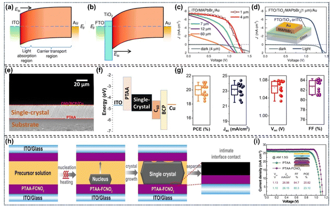 |
| | Fig. 16 Configuration and performances of single-crystalline perovskite-based solar cells: (a and b) band alignment diagrams for ITO/MAPbBr3/Au and FTO/TiO2/MAPbBr3/Au configurations; (c and d) dark and illuminated J–V curves of ITO-based and FTO/TiO2-based monocrystalline solar cells.82 Copyright 2016, Wiley-VCH. (e and f) Cross-sectional SEM image and band alignment of a single-crystalline MAPbI3 based solar cells; (g) statistical analysis of photovoltaic parameters of single-crystalline PSCs based on 12 devices.152 Copyright 2019, American Chemical Society. (h) Schematic illustration of crystal nucleation and growth in confined spaces via in situ growth with PTAA-FCNO2 HTLs; (i) J–V curves of single-crystal PSCs under AM1.5 light illumination (inset shows the device architecture).7 Copyright 2025, Wiley-VCH. | |
Table 4 Summary of photovoltaic parameters of perovskite single-crystal solar cells
| Device structure |
J
SC [mA cm−2] |
V
OC [V] |
FF |
PCE [%] |
Ref. |
| ITO/PEDOT:PSS/MAPbI3 arrays/PCBM/ZnO/Al |
8.69 |
0.52 |
0.379 |
1.73 |
51
|
| ITO/PEDOT:PSS/MAPbI3/PCBM/Ag |
22.15 |
0.75 |
0.270 |
4.40 |
69
|
| FTO/Cu/Au/Ag/LiF/PCBM//MAPbI3/Spiro-MeOTAD/ITO/Au |
≈13.5 |
1.15 |
≈0.296 |
≈4.50 |
92
|
| Au/MAPbI3/Au |
2.28 |
0.82 |
≈0.710 |
5.36 |
77
|
| FTO/TiO2/MAPbBr3/Au |
6.96 |
1.36 |
0.690 |
6.53 |
82
|
| FTO/TiO2/MAPbI3/Spiro-MeOTAD/Ag |
22.28 |
0.66 |
0.590 |
8.78 |
49
|
| ITO/NiOX/(FAPbI3)0.85(MAPbBr3)0.15/TiO2/Ag |
23.14 |
1.03 |
0.510 |
12.18 |
52
|
| ITO/Cu:NiOX/(TEA)2(MA)2Pb3I10/PCBM/Ag |
15.85 |
1.23 |
0.753 |
14.68 |
53
|
| ITO/PTAA/MAPbI3/PCBM/C60/BCP/Cu |
21.00 |
1.08 |
0.786 |
17.80 |
84
|
| ITO/PTAA/MAPbI3/C60/BCP/Cu |
23.46 |
1.07 |
0.835 |
21.09 |
152
|
| ITO/MeO-2PACz SAM/FA0.6MA0.4PbI3/C60/BCP/Cu |
27.50 |
1.07 |
0.770 |
23.10 |
167
|
| ITO/SAM/PTAASAM/MAPbI3/C60/BCP/Cu |
25.41 |
1.143 |
0.831 |
24.12 |
202
|
| ITO/MeO-2PACz/Cs0.05FA0.95PbI3/C60/BCP/Cu |
28.07 |
1.091 |
0.793 |
24.29 |
203
|
| ITO/HTL/Cs0.05FA0.95PbI3/C60/BCP/Cu |
26.15 |
1.10 |
0.803 |
25.80 |
7
|
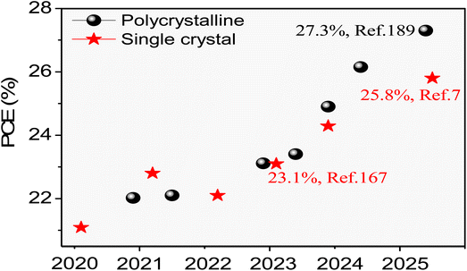 |
| | Fig. 17 Notable efficiency evolution of single-junction p–i–n perovskite polycrystalline and single-crystal solar cells since 2020.189–197 Copyright 2025, Progress in Photovoltaics: Research and Applications. | |
4.3. High-energy ray detectors
As ideal light-absorbing materials, single-crystal perovskites not only exhibit exceptional performance in photodetectors and solar cells but also show significant promise in high-energy ray detection, with applications spanning computed tomography, medical diagnostics, industrial nondestructive testing, and security screening systems. Their superior performance arises from three key advantages.
4.3.1. Large absorption coefficient.
The integration of high atomic number elements (e.g., Pb, I, Br) in single-crystal perovskites endows them with strong absorption capabilities for high-energy photons (X-rays, γ-rays). This is attributed to the dependence of the X-ray attenuation coefficient αon atomic number Z of the material, following the relationship α ∝ Z4/E3, where E is the X-ray photo energy. Additionally, their linear attenuation coefficients are comparable to those of traditional scintillators such as CsI:Tl.153
4.3.2. Superior optoelectronic performance.
The intrinsic low defect density of the single-crystal structure endows these materials with near-unity photoluminescence quantum yields, low trap densities, high charge carrier mobility, short fluorescence decay times (sub-nanoseconds to nanoseconds), and outstanding light yields (surpassing 30000 photons per MeV in certain cases). These properties enable them to meet the rigorous requirements for rapid response and high sensitivity in high energy ray detection.154–156
4.3.3. Simple solution processability and bandgap tunability.
Single-crystal perovskites can be synthesized through low temperature solution-based methods and exhibit tunable bandgaps. This allows optimization for specific detection wavelengths and facilitates their integration into flexible or large area devices.157–159
As early as 2016, Huang's group pioneered an MAPbBr3 single-crystal-based X-ray detector, which showed approximately 33–42% and 16.4% detection efficiency for UV-vis light and X-ray photons, respectively. As shown in Fig. 18a–d, the device adopts a typical p–i–p configuration structure, with charge generation induced by both light and X-ray excitation. Notably, its sensitivity reached 80 µC Gyair−1 cm−2, surpassing commercial detectors by significant margins: 10 times that of the Cd(Zn)Te single crystal X-ray detector, 4 times that of α-Se X-ray detectors, and 70 times that of polycrystalline perovskite X-ray detectors.16 In the same year, Kovalenko's group demonstrated that solution-grown MAPbI3, FAPbI3, and I-treated MAPbBr3 single crystals could serve as room-temperature, direct-conversion solid-state gamma-detecting materials. They further noted that although FAPbI3 single crystal exhibits thermodynamic instability, it is still viable for the testing, and detectors based on FAPbI3 showed optimal detection performance.157 Concurrently, Wei et al. obtained a high resolution 137Cs gamma-ray energy spectrum using an MAPbBr2.94Cl0.96 single-crystal detector under a modest electric field of 1.8 V mm−1 at room temperature. The spectral resolution surpassed that of conventional scintillator-based detectors.158 Additionally, Liu et al. developed a high sensitivity X-ray detector based on the (BDA)PbI4 (BDA = NH3C4H8NH3) single crystal synthesized in aqueous solution via a modified temperature crystallization method. The Schottky-type detector exhibited a remarkable sensitivity of 242 µC Gyair−1 cm−2 under a 10 V bias (0.31 V µm−1), surpassing Pb-free Cs2AgBiBr6 (105 µC Gyair−1 cm−2, 25 V mm−1) and MAPbBr3 single crystals (80 µC Gyair−1 cm−2) by factors of 2.3 and 3.0, respectively (Fig. 18e–g).159 Subsequently, the Kanatzidis research group demonstrated an all-inorganic CsPbBr3 single crystal detector fabricated through a low-cost solution growth process, achieving superior material quality characterized by low defect density and excellent short-range order. The eutectic gallium indium/CsPbBr3/Au Schottky diode structure attained a record-high X-ray sensitivity exceeding 10000 µC Gyair−1 cm−2 with an ultra-low detection limit of 22 nGyair s−1. Notably, the device maintained excellent photocurrent linearity and reproducibility under synchrotron X-ray irradiation (58.61 keV, 106–1010 photons s−1 mm−2), demonstrating its operational stability in extreme radiation environments (Fig. 18h–k).160 In a recent breakthrough, Liu et al. demonstrated Cs+-doped MAPbI3 single crystals exhibiting superior X-ray detection performance through systematic investigation of dopant-induced modifications in crystal lattice symmetry, defect population distribution, bandgap alignment, ion migration barriers, and carrier transport kinetics. The fabricated detectors achieved unprecedented detection metrics, including a high sensitivity of 49847 µCGyair−1 cm−2, low detection limit of 3.1 nGyair s−1, short response rise time of 150 µs, coupled with exceptional long-term stability (>10000 s continuous operation under X-ray irradiation and bias) as evidenced by the invariant response current curves shown in Fig. 18l–n.161
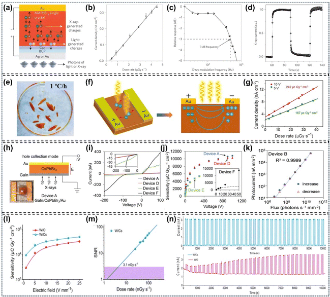 |
| | Fig. 18 Characteristics of single-crystal perovskite-based X-ray detectors: (a–d) device architecture and performance metrics of single-crystalline perovskite X-ray detectors.16 Copyright 2016, Springer Nature. (e) Photograph of (BDA)PbI4 single crystals grown at 30 °C min−1 ramp rate; (f) schematic of planar X-ray detector geometry and electric field distribution; (g) X-ray induced response current across varying dose rates, with sensitivity extracted from the slope of the linear fit.159 Copyright 2020, Wiley-VCH. (h) Schematic of the CsPbBr3 detector structure and experimental test configuration; (i–k) dark I–V characteristics, X-ray sensitivity, and photocurrent calculations under different X-ray flux conditions for CsPbBr3 devices.160 Copyright 2023, Wiley-VCH. (l–n) Comparative analysis of sensitivity, SNR, and X-ray on/off response currents for W/Cs SC and W/O SC detectors.161 Copyright 2025, Wiley-VCH. | |
X-ray detectors are categorized into two types: direct and indirect. Direct detectors utilize ionized materials to convert high-energy radiation directly into electrical signals. Indirect detectors, by contrast, employ scintillators to transform X-rays into low-energy photons, which are subsequently captured by an arrayed photodetector to produce imaging. In 2016, Birowosuto and colleagues conducted a study on the X-ray scintillation properties of (EDBE)PbCl4, MAPbI3 and MAPbBr3 single crystals. Through low temperature X-ray excited luminescence measurements, they discovered that the X-ray luminescence yield could reach up to approximately 120000 photons per MeV for (EDBE)PbCl4 at a temperature of 130 K, and exceed 150000 photons per MeV for both MAPbI3 and MAPbBr3 at 10 K. Notably, the light yield of the 3D perovskites MAPbI3 and MAPbBr3 dropped sharply at room temperature, falling below 1000 photons per MeV, whereas the 2D perovskite (EDBE)PbCl4 was less affected, maintaining a yield of around 9000 photons per MeV (Fig. 19a–c). This significant temperature dependence is attributed to the thermal quenching behavior in the 3D perovskite, while the 2D perovskite mitigates this effect due to its large exciton binding energy.162 Subsequently, Xu's team investigated the room temperature scintillation properties of MAPbCl3−xBrx crystals, and identified that those with high emission-weighted longitudinal transmittance (EWLT) hold promise for scintillator applications.163–165 Specifically, the MAPbBr0.05Cl2.95 crystal exhibits an outstanding EWLT of 90%, significantly outperforming the 57.2% EWLT achieved by LYSO. Moreover, this crystal demonstrates a superior light yield of 18000 photons per MeV and an exceptionally short decay time of 0.14 ± 0.02 ns, surpassing the MAPbCl3 crystal in these aspects (Fig. 19d–f).166 Additionally, a formic acid-assisted metastable crystallization approach was proposed by Zhu et al. for the fabrication of high-quality MAPbBr3 single crystals. The X-ray detectors constructed from these crystals exhibit a remarkable sensitivity of 2975.7 µC Gyair−1 cm−2 under a −20 V bias, coupled with a minimal detectable X-ray dose rate of 0.48 µGyair−1, which is approximately 11 times lower than the threshold value of 5.5 µGyair−1 required for routine medical diagnostic applications.167 Liu et al. proposed an airflow-controlled solvent evaporation (ACSE) strategy for the room-temperature growth of large-sized 2D layered perovskite (PEA)2PbBr4 single crystals, and systematically investigated their X-ray scintillation performance. Under X-ray excitation, the (PEA)2PbBr4 single crystal demonstrates a high light yield of 73226 photons per MeV and a fast response time of 14 ns, which are approximately 1.4 times and 75 times superior to those of the commercial CsI:Tl scintillator (54000 photons per MeV and 1049 ns), respectively. Based on these prominent characteristics, an X-ray imager was constructed by integrating a (PEA)2PbBr4 single crystal, achieving a high spatial resolution of 11.1 lp mm−1 in X-ray imaging (Fig. 19g–i).168 Meanwhile, Song et al. reported a novel scintillation material, namely CsPbClxBr3−x:Yb3+ quantum cutting scintillator, which features a PLQY of 149% and a Stokes shift exceeding 550 nm. This material successfully overcomes the issues of poor PLQY caused by thermal quenching and large self-absorption in 3D perovskite SCs. Moreover, the scintillators exhibit high transmittance, large X-ray absorption/conversion efficiency, an outstanding light yield of 112281 photons per MeV, and a detection limit as low as 176.5 nGyair s−1, and enable high-contrast single-pixel X-ray imaging (Fig. 19j and k).169 Recently, Gao et al. prepared a series of deuterated MAPbI3-based X-ray detectors (DxMAPbI3, x = 0, 0.15, 0.75, 0.99), and improved their performances by tuning deuterium content in organic cations. The D0.99MAPbI3 SC detector exhibits a more than five-fold performance enhancement, featuring a record µτ product (5.39 × 10⁻² cm2 V−1), ultrahigh sensitivity (2.18 × 10⁶ µC Gy−1 cm−2 at 120 keV), low detection limit (4.8 nGyair s−1) and long-term stability, offering a straightforward route to advanced perovskite X-ray detection systems.170 Zhao and his research team made a notable breakthrough by successfully synthesizing inch-sized (PEA)2PbBr4 SCs (4.60 cm ×3.80 cm ×0.19 cm) using a combined approach of evaporation crystallization and nucleation-controlled strategies. These (PEA)2PbBr4 SCs demonstrated exceptional scintillation performance, characterized by high light yields of 38600 photons per MeV and ultra-fast decay times (4.89 ns under a 375 nm laser, 27.98 ns under γ-ray exposure, and 3.84 ns under α-particle bombardment). For X-ray imaging, the (PEA)2PbBr4 SCs achieved a spatial resolution of 23.2 lp mm−1 at a modulation transfer function of 20%. Additionally, they set a record resolution of 2.00 lp mm−1 for fast neutron imaging, marking the highest resolution achieved by perovskite scintillators to date (Fig. 19l and m). X-ray imaging tests were conducted using a ballpoint pen, a 2.72 cm spring, and a 0.60 cm spring, all encapsulated within a polytetrafluoroethylene triangular prism as test objects. As illustrated in Fig. 19n, the radiographs clearly depicted the ballpoint pen tip and the springs, highlighting the outstanding non-destructive detection capabilities of the (PEA)2PbBr4 SCs.171
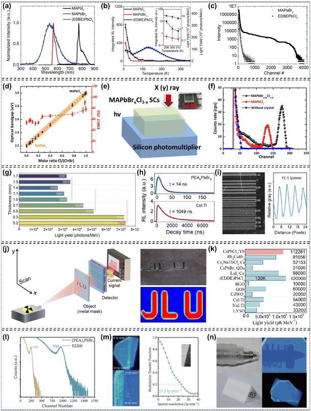 |
| | Fig. 19 Scintillation properties of single-crystal perovskites: (a–c) comparison of normalized X-ray excited luminescence spectra, light yield temperature dependence, and pulse height spectra.162 Copyright 2016, Springer Nature. (d) Optical band gap, integrated XEL light yield, and EWLT versus Cl/(Br + Cl) molar ratio; (e and f) pulse height spectra and schematic of MAPbBrxCl3−x SCs integrated on the window of SiPM.166 Copyright 2018, American Chemical Society. (g–i) Light yield SC thickness dependence, RL decay time, and X-ray line chart image of the (PEA)2PbBr4 scintillator.168 Copyright 2023, American Chemical Society. (j and k) Single pixel X-ray imaging and light yield of CsPbCl3:Yb3+ scintillators.169 Copyright 2023, Wiley-VCH. (l–n) Pulse height spectra, modulation transfer function curves, photographs and X-ray images of encapsulated objects.171 Copyright 2025, Wiley-VCH. | |
4.4. Light-emitting diodes and lasers
Lead halide perovskite single crystals excel as high-performance light-absorbing materials, with broad application prospects not only in solar cells and photodetectors but also across diverse optoelectronic fields such as light-emitting diodes (LEDs) and lasers. This exceptional versatility stems primarily from their superior photoluminescence efficiency, low bulk defect density, suppressed Auger recombination rates, and ability for long-range, balanced ambipolar charge transport. The research on single-crystal perovskite light-emitting diodes (PeLEDs) originated in 2014, when Tan et al. first reported green and red light-emitting devices based on CH3NH3PbI3−xClx perovskite.172 Since then, extensive efforts have been devoted to enhancing the quantum efficiency of PeLEDs, including optimizing the crystalline quality of the perovskite luminescent layer and improving the performance of electron/hole transport layers.57,173–176 However, PeLED development is significantly constrained by incoherent light emission arising from random crystal domain orientations in polycrystalline perovskite thin films. Consequently, single-crystal perovskite-based LEDs demand urgent development, serving as a crucial milestone for electrically driven laser diodes.177
In 2015, the Gao group successfully fabricated efficient and bright green LEDs utilizing single-crystalline, highly emissive MAPbBr3 nanoplatelets. This achievement was primarily attributed to the inherent properties of the single-crystal nanoplatelets and the introduction of composition-tailored bipolar host materials. Further investigation revealed that the as-prepared perovskite nanomaterials exhibited high stability and moisture resistance in ambient air, enabling glovebox-free fabrication of LED devices.178 Subsequently, Yu's group designed LEDs based on perovskite single-crystalline micro-platelets, adopting a simple ITO/MAPbBr3/Au device structure. This device could be turned on at 1.8 V and operate for 54 h under a luminance of approximately 5000 cd m−2 without any noticeable degradation in brightness (Fig. 20a–d).177 Nguyen et al. fabricated a green luminescence device with a simple ITO/MAPbBr3/ITO structure. The finding of photoluminescence blinking behavior at the crystal edges may provide new insights into the recombination processes depending on the carrier traps and defects of emission layers in perovskite light-emitting devices.178 Simultaneously, Gao et al. obtained a high quality MAPbBr3 film consisting of micron-scale single crystals by utilizing benzophenone as a crystallizing agent, and applied this film to PeLED fabrication. Compared with the control device, the device showed enhanced performance, achieving a maximum luminance of 1057.6 cd m−2 and a turn-on voltage of 2.25 V.179 Recently, Jie et al. proposed a convenient and efficient liquid-insulator bridging strategy to fabricate high-luminance green PSC-based LEDs using CH3NH3PbBr3 microflakes. A blade-coated poly(methyl methacrylate) insulating layer mitigated leakage current and short circuits, enabling reliable PSC-LED fabrication. The device exhibited an ultrahigh luminance of 136100 cd m−2 and a half-lifetime of 88.2 min at an initial luminance of ∼1100 cd m−2. Additionally, the microflake-based PSC-LEDs exhibited strong polarized edge emission with a high degree of polarization reaching up to 0.69 (Fig. 20e–h).180 Meanwhile, Chen et al. developed an LED based on bare perovskite single-crystal films that achieved high performance without relying solely on surface passivation and interface modification. The device achieved a brightness exceeding 10000 cd m−2 and an EQE of ∼1.3%. Moreover, their electroluminescence peak was centered at 521 nm with a full width at half maximum of 18 nm, which fully meets the display requirements of the National Television System Committee standard. The device also exhibited good stability, their T50 reached over 2 h and 37 h at 1000 cd m−2 and 100 cd m−2 initial luminance, respectively.181
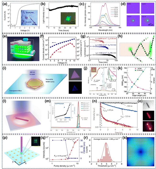 |
| | Fig. 20 Characteristics of single-crystal perovskite-based LEDs and lasers: (a–d) I–V curve, stability pattern, electroluminescence spectra, and microscopic optical images of an MAPbBr3 microplatelet-based LED.177 Copyright 2017, American Chemical Society. (e–h) Device construction, L–V–J curves, operational stability, and schematic of polarized emission generation for PSC-LEDs.180 Copyright 2022, American Chemical Society. (i–k) Schematic illustration of perovskite whispering-gallery-mode nanocavities and their corresponding lasing characterization.186 Copyright 2014, American Chemical Society. (l–o) Schematic illustration, lasing threshold emission spectra, optical images, and time resolved photoluminescence decay kinetics of near-infrared lasing from single crystal MAPbI3 nanowires.15 Copyright 2015, Springer Nature. (p) Schematic illustration of an individual MAPbBr3 microplate excited by a 395 nm laser; (q) integrated PL emission intensity (red) and FWHM (blue) of PL peaks versus pump density; (r) lasing threshold statistics of MAPbBr3 microplate arrays; (s) FDTD simulations of whispering gallery modes.187 Copyright 2023, Springer Nature. | |
Lead halide perovskite single crystals have low trap state density, long electron–hole diffusion length, high carrier mobility, and extended carrier lifetime, making them ideal for laser devices with low lasing thresholds and high qualities.15,41,182,184 For example, Hou et al. devised an antisolvent-free strategy for fabricating MAPbBr3 single-crystal microdisks with square and octagonal morphologies. Specifically, a trace amount of N-methyl-2-pyrrolidone (NMP) was incorporated into the perovskite precursor solution to decelerate the crystallization kinetics during spin-coating. The resultant MAPbBr3 microdisks enabled whispering gallery mode (WGM) lasing, exhibiting excellent laser performance with a threshold value below 50 mJ cm−2 and a quality factor exceeding 1000.183 Yan et al. prepared MAPbBr3 single-crystal microcavities by integrating template-limited growth with antisolvent diffusion methods, yielding microcavities with tunable geometries and sizes. These single-crystal microcavities emitted laser light at ≈550 nm under femtosecond laser pumping, displaying a lasing threshold of ≈35 µJ cm−2, a quality factor of 1135, as well as outstanding long-term operational stability.184 Recently, Sum group's research revealed that MAPbX3 (X = Cl, Br, I) perovskites serve as highly promising gain media, endowed with a range of desirable properties. Notably, lasing behavior in MAPbI3 single crystals was successfully induced through the utilization of specifically designed cavity resonators. Furthermore, the inherently low bulk defect density characteristic of MAPbI3 films plays a pivotal role in achieving reduced amplified spontaneous emission thresholds, alongside facilitating long-range, balanced charge carrier diffusion lengths.185 Subsequently, Xiong's group has made significant advancements in the realm of low-threshold NIR nanolasers, successfully realizing NIR lasing by employing CH3NH3PbI3−aXa (X = Cl, Br, I) nanoplatelets integrated within a distributed Bragg reflector (DBR) cavity. Notably, their experiments showed a typical MAPbI3 triangular nanoplatelet with a low lasing threshold of 37 µJ cm−2 and a quality factor of 650 (Fig. 20i–k).186 Adopting a similar approach, Liao et al. designed a novel single-crystalline laser, which utilizes the four side faces of square MAPbBr3 microdisks as a built-in whispering-gallery mode microresonator. This laser achieved a low threshold of 3.6 µJ cm−2, a quality factor of 430, and emitted light at a wavelength of 557.5 nm from the four side-faces of the square MAPbBr3 microdisk.146 Additionally, the Zhu group developed wavelength-tunable single crystal MAPbX3 (X = Br, I) nanowire lasers, with a threshold of 220 nJ cm−2 and a quality factor of 3600 (Fig. 20l–o).15 Jin's group successfully prepared high-quality FAPbX3 (X = Br, I) and MABr-stabilized FAPbI3 single-crystal nanowires via low-temperature solution growth. These nanowires showed superior photostability and longer wavelength tunability compared to MA-based perovskites, and the corresponding nanowire exhibited a lasing threshold of approximately several µJ cm−2 and a quality factor of ∼2000.17 Recently, Pan et al. successfully synthesized high-quality single-crystalline MAPbBrxCl3−x (MA = CH3NH3, x = 0, 1, 2, 3) microplate arrays. These perovskite microplates serve as high-quality microcavities for whispering gallery mode lasing, demonstrating a high-quality factor of 2915 and a low threshold of 4.14µJ cm−2. Importantly, the lasing mode can be precisely tuned by adjusting the dimensions of the microplates (Fig. 20p–s).187 In a separate study, Chen et al. developed a high-performance vertical cavity surface emitting laser (VCSEL) via a simple solution process. The device uses a highly crystalline CsPbBr3 single-crystal microplatelet, which is sandwiched between two distributed Bragg reflector. Under 400 nm femtosecond optical pumping, this VCSEL achieves single-mode lasing at 542 nm, with a low threshold power density of 5 µJ cm−2 and a high-quality factor of 2893.188
5. Conclusion and outlook
In this review, we present a thorough overview of the remarkable advancements achieved in the field of lead halide perovskite single crystals, encompassing their fundamental properties, growth techniques, and device applications. Numerous studies have confirmed that single-crystalline perovskites outperform polycrystalline thin-film counterparts in terms of photoelectric performance, primarily due to their extremely low defect densities and few interface defects. Moreover, these materials exhibit superior thermal and ambient stability, rendering them ideal candidates for high-stability optoelectronic devices while enabling in-depth exploration of the intrinsic properties of perovskite materials. Nevertheless, several long-standing challenges in this field remain to be addressed and overcome by researchers. We believe that in-depth research into the following aspects will provide researchers with substantial benefits and innovative insights, driving performance optimization of single-crystalline perovskites and accelerating the development of related optoelectronic devices.
(1) Manufacturing challenges: compared to bulk single-crystal perovskites, single-crystalline thin films are better suited for direct use in a wide range of vertical-type optoelectronic devices. However, the preparation of single-crystalline perovskite thin films that simultaneously feature submicron thickness and large lateral dimensions continues to pose a significant challenge. Initially, researchers adopted a slicing process to obtain the desirable materials, but this method led to serious material loss and required multiple necessary post-treatment processes. Later, the space confinement method emerged as an efficient alternative, yet it has drawbacks, such as extensive organic solvent use and difficulty in accurately controlling nucleation rate. Therefore, a dual-pronged strategy is imperative to fabricate high-quality single-crystalline perovskite thin films with precisely controllable morphology and dimensions going forward. On the one hand, new and universal growth methods tailored specifically to these thin films should be vigorously explored and developed. On the other hand, the refinement and upgrading of immature solution-based techniques are of equal importance, which entails innovating and optimizing the instrumentation for space-confined single crystal growth, as well as leveraging template-seeded directional growth strategies to precisely modulate the thickness and dimensions of the target thin films, thereby satisfying the stringent requirements of advanced optoelectronic applications.
(2) Defects and nonradiative carrier losses: with inherent merits including ultralow defect density, extended carrier diffusion length and elevated ion migration barrier, single-crystal perovskites exhibit immense potential in diverse optoelectronic applications. Although significant breakthroughs have been realized in high-energy ray detectors and laser technologies, the efficiency of single-crystal perovskite solar cells remains inferior to that of polycrystalline thin-film solar cells. This efficiency disparity is primarily attributable to the high surface/interface defect states in single-crystal perovskites, as well as the incomplete interface contact between the perovskite layer and charge transport layers/substrate, both of which induce carrier nonradiative recombination and consequent efficiency loss. Accordingly, the following targeted strategies can be implemented to elevate the efficiency of perovskite single-crystal solar cells. (i) Devise effective surface passivation approaches, such as using organic cations to passivate the uncoordinated halogen or lead ion defects on the crystal surface. (ii) Adopt appropriate additives and nucleation technologies, for instance, regulating crystal growth by leveraging Lewis acids and bases; alternatively, enabling in situ nucleation and growth of crystals with organic amine salts (e.g., PEA+, EA+, NHMS and FCNO2) to reduce defects. (iii) Optimize device fabrication processes to enhance the contact between single-crystal perovskites and substrates, such as suppressing the carrier recombination loss in single-crystal devices via doping, energy level optimization, surface/interface defect passivation and other related methods.
(3) Stability issues: it is of utmost importance to thoroughly address the challenges related to long-term stability, encompassing both thermal and environmental stability, in perovskite-based optoelectronic devices. Although compared with perovskite polycrystalline thin films, single-crystalline perovskite exhibited better performance through applying the interface engineering and passivating technique, they remain limited by insufficient long-term stability. Future research should prioritize the development of stable perovskite compositions, which includes constructing mixed-halides (e.g., MAPb(Br/I)3) or mixed-cation (e.g., (Cs/FA)1PbI3) single-crystal systems or incorporating anti-degradation stabilizing additives. A deeper insight into degradation pathways, especially halide ion migration and phase transition, is essential for enhancing long-term stability. Given the critical impact of lattice defects on material stability, exploring defect-mitigation strategies (e.g., doping organic cations, Lewis acids/bases, and optimizing precursor solution concentration) will underpin the practical long-term application of perovskite materials. Additionally, the inherent toxicity concerns associated with Pb-based perovskites warrant careful and comprehensive consideration. This issue constitutes the most formidable barrier that hinders their large-scale commercialization. Consequently, there is an urgent demand for Pb-free, low-toxicity single-crystal perovskites with robust long-term stability in the highly efficient photoelectric device field.
(4) Device integration difficulties: single-crystal perovskite materials have a defect density two to three orders of magnitude lower than that of their polycrystalline counterparts, positioning them as a highly promising light-absorbing layer for photovoltaic applications. Nevertheless, the PCE of solar cells based on single-crystal perovskites currently falls short of that achieved by their polycrystalline counterparts. This efficiency gap primarily stems from the relatively late development of single-crystal materials, which renders their integration with established photovoltaic technologies highly challenging. The structural design of existing high-efficiency perovskite solar cells, along with the selection of electrode and charge transport layer materials, is optimized primarily for polycrystalline perovskite materials and their charge transport characteristics. Although single-crystal perovskites possess superior charge mobility and longer carrier lifetime, mismatched energy levels and high interfacial barriers in the current device structures fail to exploit these advantages, limiting charge extraction and collection efficiency. Therefore, future research should focus on designing device structures tailored to the characteristics of single crystals. Specifically, based on the unique charge transport properties of single-crystal perovskites, charge transport layer materials with matched energy levels need to be selectively adopted and the thickness and doping concentration of the transport layers adjusted. Meanwhile, novel device architecture such as the p–i–n inverted structure needs to be explored to accelerate the rate of charge extraction and collection, giving full play to the advantages of low defect density in single-crystal materials. Furthermore, single crystal preparation equipment compatible with existing polycrystalline production lines should be developed to reduce production line transformation costs.
Author contributions
All of the authors contributed to the literature search, writing and editing of this review.
Conflicts of interest
There are no conflicts to declare.
Data availability
No primary research results, software, or code have been included, and no new data were generated or analysed as part of this review.
Acknowledgements
This work was supported by the National Natural Science Foundation of China (Grant No. 12404458, 62222502, and U2441222), the Natural Science Foundation of Inner Mongolia (2024QN02025), the Key Scientific Research Project Plan of Colleges and Universities in Henan Province (25A140016), the “Yingcai Xingmeng” Team Project (No. 2025TYL06), and Research Foundation for Advanced Talents of Inner Mongolia Normal University (2025YJRC011).
References
- H. L. Wells, Z. Anorg. Allg. Chem., 1893, 3, 195–210 CrossRef.
- H. F. Kay and P. C. Bailey, Acta Cryst., 1957, 10, 219–226 CrossRef CAS.
- J. Chen and N. G. Park, Adv. Mater., 2019, 31, 1803019 Search PubMed.
- J. Ding and Q. Yan, Sci. China Mater., 2017, 60, 1063–1078 CrossRef CAS.
- T. Leijtens, E. T. Hoke, G. Grancini, D. J. Slotcavage, G. E. Eperon, J. M. Ball, M. D. Bastiani, A. R. Bowring, N. Martino, K. Wojciechowski, M. D. McGehee, H. J. Snaith and A. Petrozza, Adv. Energy Mater., 2015, 5, 1500962 Search PubMed.
- J. Z. Song, Q. Z. Cui, J. H. Li, J. Y. Xu, Y. Wang, L. M. Xu, J. Xue, Y. H. Dong, T. Tian, H. D. Sun and H. B. Zeng, Adv. Opt. Mater., 2017, 5, 1700157 Search PubMed.
- N. Q. Liu, M. X. Liu, J. T. Dai, X. Cheng and Z. L. Chen, Angew. Chem., Int. Ed., 2025, 64, e202500947 CrossRef CAS.
- Z. Z. Chang, Z. J. Lu, W. Deng, Y. D. Shi, Y. Y. Sun, X. J. Zhang and J. S. Jie, Nanoscale, 2023, 15, 5053–5062 Search PubMed.
- N. Ding, H. L. Liu, Y. Q. Liu, D. G. Li, M. Y. Yao, Y. N. Ji, G. Zhu, R. Xue and W. Xu, Laser Photonics Rev., 2025, 202500887 Search PubMed.
- K. Grover, J. S. Choudhary, P. Dhawan, R. Jha and H. Yadav, J. Phys. Chem. Solids, 2025, 203, 112713 CrossRef CAS.
- R. H. Mao, L. Y. Zhang and R. Y. Zhu, IEEE Trans. Nucl. Sci., 2012, 59, 2224–2228 CAS.
- Q. Xu, H. T. Wei, W. Wei, W. Chuirazzi, D. DeSantis, J. S. Huang and L. Cao, Nucl. Instrum. Methods Phys. Res. A, 2017, 848, 106–108 Search PubMed.
- H. J. Fang, Q. Li, J. Ding, N. Li, H. Tian, L. J. Zhang, T. L. Ren, J. Y. Dai, L. D. Wang and Q. F. Yan, J. Mater. Chem. C, 2016, 4, 630–636 Search PubMed.
- B. W. H. Baugher, H. O. H. Churchill, Y. F. Yang and P. J. Herrero, Nat. Nanotechnol., 2014, 9, 262–267 CrossRef CAS.
- H. M. Zhu, Y. P. Fu, F. Meng, X. X. Wu, Z. Z. Gong, Q. Ding, M. V. Gustafsson, M. T. Trinh, S. Jin and X. Y. Zhu, Nat. Mater., 2015, 14, 636–642 CrossRef CAS PubMed.
- H. T. Wei, Y. J. Fang, P. Mulligan, W. Chuirazzi, H. H. Fang, C. C. Wang, B. R. Ecker, Y. L. Gao, M. A. Loi, L. Cao and J. S. Huang, Nat. Photonics, 2016, 10, 333–339 CrossRef CAS.
- Y. P. Fu, H. M. Zhu, A. W. Schrader, D. Liang, Q. Ding, P. Joshi, L. Hwang, X. Y. Zhu and S. Jin, Nano Lett., 2016, 16, 1000–1008 CrossRef CAS.
- F. Cao, J. D. Chen, D. J. Yu, S. Wang, X. B. Xu, J. X. Liu, Z. Y. Han, B. Huang, Y. Gu, K. L. Choy and H. B. Zeng, Adv. Mater., 2020, 32, 1905362 CrossRef CAS.
- J. M. Chen, R. H. Mao, L. Y. Zhang and R. Y. Zhu, IEEE Trans. Nucl. Sci., 2007, 54, 718–724 Search PubMed.
- X. Gong, M. H. Tong, Y. J. Xia, W. Z. Cai, J. S. Moon, Y. Cao, G. Yu, C. L. Shieh, B. Nilsson and A. J. Heeger, Science, 2009, 325, 1665–1667 Search PubMed.
- J. H. Noh, S. H. Im, J. H. Heo, T. N. Mandal and S. I. Seok, Nano Lett., 2013, 13, 1764–1769 CrossRef CAS PubMed.
- J. S. Park, S. Choi, Y. Yan, Y. Yang, J. M. Luther, S. H. Wei, P. Parilla and K. Zhu, J. Phys. Chem. Lett., 2015, 6, 4304–4308 CrossRef CAS PubMed.
- C. Rodà, A. L. Abdelhady, J. Shamsi, M. Lorenzon, V. Pinchetti, M. Gandini, F. Meinardi, L. Manna and S. Brovrlli, Nanoscale, 2019, 11, 7613–7623 RSC.
- J. N. Chen, S. S. Zhou, S. Y. Jin, H. Q. Li and T. Y. Zhai, J. Mater. Chem. C, 2016, 4, 11–27 Search PubMed.
- H. W. Zhou, Z. H. Nie, J. Yin, Y. W. Sun, H. Y. Zhuo, D. Q. Wang, D. C. Li, J. M. Dou, X. X. Zhang and T. L. Ma, RSC Adv., 2015, 5, 85344–85349 RSC.
- M. Y. Luan, J. L. Song, X. F. Wei, F. Chen and J. H. Liu, CrystEngComm, 2016, 18, 5257–5261 RSC.
- Y. Tidhar, E. Edri, H. Weissman, D. Zohar, G. Hodes, D. Cahen, B. Rybtchinski and S. Kirmayer, J. Am. Chem. Soc., 2014, 136, 13249–13256 Search PubMed.
- M. Y. Chen, H. Yu, S. V. Kershaw, H. H. Xu, S. Gupta, F. Hetsch, A. L. Rogach and N. Zhao, Adv. Funct. Mater., 2014, 24, 53–59 CrossRef CAS.
- Q. Q. Lin, A. Armin, P. L. Burn and P. Meredith, Laser Photonics Rev., 2016, 10, 1047–1053 CrossRef CAS.
- C. X. Bao, Z. L. Chen, Y. J. Fang, H. T. Wei, Y. H. Deng, X. Xiao, L. L. Li and J. S. Huang, Adv. Mater., 2017, 29, 1703209 CrossRef PubMed.
- B. C. Yu, J. J. Shi, Y. M. Li, S. Tan, Y. Q. Cui, F. Q. Meng, H. J. Wu, Y. H. Luo, D. M. Li and Q. B. Meng, Nat. Commun., 2025, 16, 3328 CrossRef CAS.
- M. J. Yang, Y. Y. Zhou, Y. N. Zeng, C. S. Jiang, N. P. Padture and K. Zhu, Adv. Mater., 2015, 27, 6363–6370 CrossRef CAS.
- Y. H. Zhang, R. J. Sun, X. Y. Ou, K. F. Fu, Q. S. Chen, Y. C. Ding, L. J. Xu, L. M. Liu, Y. Han, A. V. Malko, X. G. Liu, H. H. Yang, O. M. Bark, H. Liu and O. F. Mohammed, ACS Nano, 2019, 13, 2520–2525 CrossRef CAS.
- H. Deng, X. K. Yang, D. D. Dong, B. Li, D. Yang, S. J. Yuan, K. Qiao, Y. B. Cheng, J. Tang and H. S. Song, Nano Lett., 2015, 15, 7963–7969 CrossRef CAS PubMed.
- H. S. Rao, B. X. Chen, X. D. Wang, D. B. Kuang and C. Y. Su, Chem. Commun., 2017, 53, 5163–5166 RSC.
- Y. X. Chen, Q. Q. Ge, Y. Shi, J. Liu, D. J. Xue, J. Y. Ma, J. Ding, H. J. Yan, J. S. Hu and L. J. Wan, J. Am. Chem. Soc., 2016, 138, 16196–16199 CrossRef CAS PubMed.
- F. Yao, J. L. Peng, R. M. Li, W. J. Li, P. B. Gui, B. R. Li, C. Liu, C. Tao, Q. Q. Lin and G. J. Fang, Nat. Commun., 2020, 11, 1194 CrossRef CAS PubMed.
- Y. C. Liu, J. K. Sun, Z. Yang, D. Yang, X. D. Ren, H. Xu, Z. P. Yang and S. Z. Liu, Adv. Opt. Mater., 2016, 4, 1829–1837 CrossRef CAS.
- Y. B. Mao, S. Banerjee and S. S. Wong, J. Am. Chem. Soc., 2003, 125, 15718–15719 CrossRef CAS PubMed.
- J. Schlipf, A. M. Askar, F. Pantle, B. D. Wiltshire, A. Sura, P. Schneider, L. Huber, K. Shankar and P. M. Buschbaum, Sci. Rep., 2018, 8, 4906 CrossRef.
- S. W. Eaton, A. Fu, A. B. Wong, C. Z. Ning and P. D. Yang, Nat. Rev. Mater., 2016, 1, 16028 CrossRef CAS.
- E. Horváth, M. Spina, Z. Szekrényes, K. Kamarás, R. Gaal, D. Gachet and L. Forró, Nano Lett., 2014, 14, 6761–6766 CrossRef.
- J. X. Ding, S. J. Du, Z. Y. Zuo, Y. Zhao, H. Z. Cui and X. Y. Zhan, J. Phys. Chem. C, 2017, 121, 4917–4923 CrossRef CAS.
- J. H. Cha, J. H. Han, W. P. Yin, C. Park, Y. M. Park, T. K. Ahn, J. H. Cho and D. Y. Jung, J. Phys. Chem. Lett., 2017, 8, 565–570 CrossRef CAS PubMed.
- I. M. Asuo, P. Fourmont, I. Ka, D. Gedamu, S. Bouzidi, A. Pignolet, R. Nechache and S. G. Cloutier, Small, 2019, 15, 1804150 CrossRef.
- Y. C. Liu, Y. X. Zhang, Z. Yang, J. S. Feng, Z. Xu, Q. X. Li, M. X. Hu, H. C. Ye, X. Zhang, M. Liu, K. Zhao and S. Z. Liu, Mater. Today, 2019, 22, 67–75 CrossRef CAS.
- Q. R. Lv, Z. P. Lian, W. H. He, J. L. Sun, Q. Li and Q. F. Yan, J. Mater. Chem. C, 2018, 6, 4464–4470 RSC.
- Y. C. Liu, Y. X. Zhang, Z. Yang, D. Yang, X. D. Ren, L. Q. Pang and S. Z. Liu, Adv. Mater., 2016, 28, 9204–9209 CrossRef CAS.
- J. J. Zhao, G. L. Kong, S. L. Chen, Q. Li, B. Y. Huang, Z. H. Liu, X. Y. San, Y. J. Wang, C. Wang, Y. C. Zhen, H. D. Wen, P. Gao and J. Y. Li, Sci. Bull., 2017, 62, 1173–1176 CrossRef CAS.
- Y. P. Fu, H. M. Zhu, J. Chen, M. P. Hautzinger, X. Y. Zhu and S. Jin, Nat. Rev. Mater., 2019, 4, 169–188 CrossRef CAS.
- T. Ye, W. F. Fu, J. K. Wu, Z. K. Yu, X. Y. Jin, H. Z. Chen and H. Y. Li, J. Mater. Chem. A, 2016, 4, 1214–1217 RSC.
- Y. Huang, Y. Zhang, J. L. Sun, X. G. Wang, J. L. Sun, Q. Chen, C. F. Pan and H. P. Zhou, Adv. Mater. Interfaces, 2018, 5, 1800224 CrossRef.
- Y. Qin, H. J. Zhong, J. J. Intemann, S. F. Leng, M. H. Cui, C. C. Qin, M. Xiong, F. Liu, A. K. Y. Jen and K. Yao, Adv. Energy Mater., 2020, 10, 1904050 CrossRef CAS.
- Y. C. Liu, Y. X. Zhang, K. Zhao, Z. Yang, J. S. Feng, X. Zhang, K. Wang, L. Meng, H. C. Ye, M. Liu and S. Z. Liu, Adv. Mater., 2018, 30, 1707314 CrossRef.
- V. M. Goldschmidt, Naturwissenschaften, 1926, 14, 477–485 CrossRef CAS.
- H. P. Rooksby, Nature, 1945, 155, 484 CrossRef CAS.
- N. K. Kumawat, A. Dey, K. L. Narasimhan and D. Kabra, ACS Photonics, 2015, 2, 349–354 CrossRef CAS.
- R. Z. Zhuang, X. J. Wang, W. B. Ma, Y. H. Wu, X. Chen, L. H. Tang, H. M. Zhu, J. Y. Liu, L. L. Wu, W. Zhou, X. Liu and Y. Yang, Nat. Photonics, 2019, 13, 602–609 CrossRef CAS.
- Y. Y. Li, G. L. Zheng, C. K. Lin and J. Lin, Solid State Sci., 2007, 9, 855–861 CrossRef CAS.
- W. Y. Zhang, Y. Y. Tang, P. F. Li, P. P. Shi, W. Q. Liao, D. W. Fu, H. Y. Ye, Y. Zhang and R. G. Xiong, J. Am. Chem. Soc., 2017, 139, 10897–10902 CrossRef CAS.
- Y. N. Chen, M. H. He, J. J. Peng, Y. Sun and Z. Q. Liang, Adv. Sci., 2016, 3, 1500392 CrossRef.
- M. Grätzel, Nat. Mater., 2014, 13, 838–842 CrossRef.
- M. A. Green, A. Ho-Baillie and H. J. Snaith, Nat. Photonics, 2014, 8, 506–514 CrossRef CAS.
- C. H. Li, K. C. K. Soh and P. Wu, J. Alloy. Compd., 2004, 372, 40–48 CrossRef CAS.
- Q. D. Sun and W. J. Yin, J. Am. Chem. Soc., 2017, 139, 14905–14908 CrossRef CAS PubMed.
- D. Weber, Z. Naturforsch. B, 1978, 33, 1443–1445 CrossRef.
- D. B. Mitzi, J. Chem. Soc., Dalton Trans., 2001, 1–12 RSC.
- N. O. Yamamuro, T. Matsuo and H. Suga, J. Phys. Chem. Solids, 1990, 51, 1383–1395 CrossRef.
- H. L. Yue, H. H. Sung and F. C. Chen, Adv. Electron. Mater., 2018, 4, 1700655 CrossRef.
- X. Li, M. I. Dar, C. Y. Yi, J. S. Luo, M. Tschumi, S. M. Zakeeruddin, M. K. Nazeeruddin, H. W. Han and M. Grätzel, Nat. Chem., 2015, 7, 703–711 CrossRef CAS.
- L. N. Quan, M. J. Yuan, R. Comin, O. Voznyy, E. M. Beauregard, S. Hoogland, A. Buin, A. R. Kirmani, K. Zhao, A. Amassian, D. H. Kim and E. H. Sargent, J. Am. Chem. Soc., 2016, 138, 2649–2655 CrossRef CAS.
- S. Bai, P. M. Da, C. Li, Z. P. Wang, Z. C. Yuan, F. Fu, M. Kawecki, X. J. Liu, N. Sakai, J. T. W. Wang, S. Huettner, S. Buecheler, M. Fahlman, F. Gao and H. J. Snaith, Nature, 2019, 571, 245–250 CrossRef CAS.
- I. C. Smith, E. T. Hoke, D. S. Ibarra, M. D. McGehee and H. I. Karunadasa, Angew. Chem., Int. Ed., 2014, 53, 11232–11235 CrossRef CAS.
- R. Wang, M. Mujahid, Y. Duan, Z. K. Wang, J. J. Xue and Y. Yang, Adv. Funct. Mater., 2019, 29, 1808843 CrossRef CAS.
- Y. L. Song, W. H. Bi, A. Wang, X. T. Liu, Y. F. Kang and Q. F. Dong, Nat. Commun., 2020, 11, 274 CrossRef CAS.
- Y. Y. Dang, Y. Liu, Y. X. Sun, D. S. Yuan, X. L. Liu, W. Q. Lu, G. F. Liu, H. B. Xia and X. T. Tao, CrystEngComm, 2015, 17, 665–670 RSC.
- Q. F. Dong, J. F. Song, Y. J. Fang, Y. C. Shao, S. Ducharme and J. S. Huang, Adv. Mater., 2016, 28, 2816–2821 CrossRef CAS PubMed.
- Q. Wang, B. Chen, Y. Liu, Y. H. Deng, Y. Bai, Q. F. Dong and J. S. Huang, Energy Environ. Sci., 2017, 10, 516–522 RSC.
- Q. F. Han, S. H. Bae, P. Y. Sun, Y. T. Hsieh, Y. M. Yang, Y. S. Rim, H. X. Zhao, Q. Chen, W. Z. Shi, G. Li and Y. Yang, Adv. Mater., 2016, 28, 2253–2258 CrossRef CAS PubMed.
- L. Chen, Y. Y. Tan, Z. X. Chen, T. Wang, S. Hu, Z. A. Nan, L. Q. Xie, Y. Hui, J. X. Huang, C. Zhan, S. H. Wang, J. Z. Zhou, J. W. Yan, B. W. Mao and Z. Q. Tian, J. Am. Chem. Soc., 2019, 141, 1665–1671 CrossRef CAS PubMed.
- M. I. Saidaminov, A. L. Abdelhady, B. Murali, E. Alarousu, V. M. Burlakov, W. Peng, I. Dursun, L. F. Wang, Y. He, G. Maculan, A. Goriely, T. Wu, O. F. Mohammed and O. M. Bakr, Nat. Commun., 2015, 6, 7586 CrossRef.
- W. Peng, L. F. Wang, M. Banavoth, K. T. Ho, A. Bera, N. C. Cho, C. F. Kang, V. M. Burlakov, J. Pan, L. Sinatra, C. Ma, W. Xu, D. Shi, E. Alarousu, A. Goriely, J. H. He, O. F. Mohammed, T. Wu and O. Bakr, Adv. Mater., 2016, 28, 3383–3390 CrossRef CAS.
- E. M. Hutter, M. C. G. Rueda, A. Osherov, V. Bulović, F. C. Grozema, S. D. Stranks and T. J. Savenije, Nat. Mater., 2017, 16, 115–120 CrossRef CAS.
- Z. L. Chen, Q. F. Dong, Y. Liu, C. X. Bao, Y. J. Fang, Y. Lin, S. Tang, Q. Wang, X. Xiao, Y. Bai, Y. H. Deng and J. S. Huang, Nat. Commun., 2017, 8, 1890 CrossRef PubMed.
- W. Peng, J. Yin, K. T. Ho, O. Ouellette, M. D. Bastiani, B. Murali, O. E. Tall, C. Shen, X. H. Miao, J. Pan, E. Alarousu, J. H. He, B. S. Ooi, O. F. Mohammed, E. Sargent and O. M. Bakr, Nano Lett., 2017, 17, 4759–4767 CrossRef CAS.
- D. Shi, V. Adinolfi, R. Comin, M. J. Yuan, E. Alarousu, A. Buin, Y. Chen, S. Hoogland, A. Rothenberger, K. Katsiev, Y. Losovyj, X. Zhang, P. A. Dowben, O. F. Mohammed, E. H. Sargent and O. M. Bakr, Science, 2015, 347, 519–522 CrossRef CAS PubMed.
- Z. Cheng, K. W. Liu, J. L. Yang, X. Chen, X. H. Xie, B. H. Li, Z. Z. Zhang, L. Liu, C. X. Shan and D. Z. Shen, ACS Appl. Mater. Inter., 2019, 11, 34144–34150 CrossRef CAS.
- H. Diab, C. Arnold, F. Lédée, G. T. Allard, G. Delport, C. Vilar, F. Bretenaker, J. Barjon, J. S. Lauret, E. Deleporte and D. Garrot, J. Phys. Chem. Lett., 2017, 8, 2977–2983 CrossRef CAS.
- N. J. Jeon, H. Na, E. H. Jung, T. Y. Yang, Y. G. Lee, G. Kim, H. W. Shin, S. Seok, J. Lee and J. Seo, Nat. Energy, 2018, 3, 682–689 Search PubMed.
- M. Pratheek and P. Predeep, Mater. Chem. Phys., 2020, 239, 122084 CrossRef.
- Q. F. Dong, Y. J. Fang, Y. C. Shao, P. Mulligan, J. Qiu, L. Cao and J. S. Huang, Science, 2015, 347, 967–970 CrossRef CAS PubMed.
- Y. C. Liu, X. D. Ren, J. Zhang, Z. Yang, D. Yang, F. Y. Yu, J. K. Sun, C. M. Zhao, Z. Yao, B. Wang, Q. B. Wei, F. W. Xiao, H. B. Fan, H. Deng, L. P. Deng and S. Z. Liu, Sci. China: Chem., 2017, 60, 1367–1370 Search PubMed.
- Y. Yang, Y. Yan, M. J. Yang, S. Choi, K. Zhu, J. M. Luther and M. C. Beard, Nat. Commun., 2015, 6, 7961 Search PubMed.
- S. D. Stranks, G. E. Eperon, G. Grancini, C. Menelaou, M. J. P. Alcocer, T. Leijtens, L. M. Herz, A. Petrozza and H. J. Snaith, Science, 2013, 342, 341–344 CrossRef CAS PubMed.
- M. I. Saidaminov, V. Adinolfi, R. Comin, A. L. Abdelhady, W. Peng, I. Dursun, M. J. Yuan, S. Hoogland, E. H. Sargent and O. M. Bakr, Nat. Commun., 2015, 6, 8724 CrossRef CAS PubMed.
- F. Y. Zhang, B. Yang, Y. J. Li, W. Q. Deng and R. X. He, J. Mater. Chem. C, 2017, 5, 8431–8435 RSC.
- L. Wang, G. D. Yuan, R. F. Duan, F. Huang, T. B. Wei, Z. Q. Liu, J. X. Wang and J. M. Li, AIP Adv., 2016, 6, 045115 CrossRef.
- M. I. Saidaminov, M. A. Haque, M. Savoie, A. L. Abdelhady, N. Cho, I. Dursun, U. Buttner, E. Alarousu, T. Wu and O. M. Bakr, Adv. Mater., 2016, 28, 8144–8149 Search PubMed.
- Z. P. Lian, Q. F. Yan, T. T. Gao, J. Ding, Q. R. Lv, C. G. Ning, Q. Li and J. L. Sun, J. Am. Chem. Soc., 2016, 138, 9409–9412 CrossRef CAS.
- Y. J. Fang, Q. F. Dong, Y. C. Shao, Y. B. Yuan and J. S. Huang, Nat. Photonics, 2015, 9, 679–686 CrossRef CAS.
- Y. X. Zhang, Y. C. Liu, Y. Y. Li, Z. Yang and S. Z. Liu, J. Mater. Chem. C, 2016, 4, 9172–9178 RSC.
- F. Y. Zhang, B. Yang, X. Mao, R. X. Yang, L. Jiang, Y. J. Li, J. Xiong, Y. Yang, R. X. He, W. Q. Deng and K. Han, ACS Appl. Mater. Interfaces, 2017, 9, 14827–14832 CrossRef CAS.
- Y. C. Liu, Z. Yang, D. Cui, X. D. Ren, J. K. Sun, X. J. Liu, J. R. Zhang, Q. B. Wei, H. B. Fan, F. Y. Yu, X. Zhang, C. M. Zhao and S. Z. Liu, Adv. Mater., 2015, 27, 5176–5183 CrossRef CAS PubMed.
- M. I. Saidaminov, A. L. Abdelhady, G. Maculan and O. M. Bakr, Chem. Commun., 2015, 51, 17658–17661 RSC.
- Y. Huang, L. Li, Z. H. Liu, H. Y. Jiao, Y. Q. He, X. G. Wang, R. Zhu, D. Wang, J. L. Sun, Q. Chen and H. P. Zhou, J. Mater. Chem. A, 2017, 5, 8537–8544 RSC.
- L. Ma, J. Dai and X. C. Zeng, Adv. Energy Mater., 2017, 7, 1601731 CrossRef.
- R. Wang, J. J. Xue, K. L. Wang, Z. K. Wang, Y. Q. Luo, D. Fenning, G. W. Xu, S. Nuryyeva, T. Y. Huang, Y. P. Zhao, J. L. Yang, J. H. Zhu, M. H. Wang, S. Tan, I. Yavuz, K. N. Houk and Y. Yang, Science, 2019, 366, 1509 CrossRef CAS.
- T. P. Zhao, R. Q. He, T. H. Liu, Y. H. Li, D. Yu, Y. X. Gao, G. Y. Qu, N. Li, C. M. Wang, H. Huang, J. Zhou, S. Bai, S. M. Xiao, Z. L. Chen, Y. M. Chen and Q. H. Song, ACS Nano, 2025, 19, 3282–3292 CrossRef CAS.
- Z. Y. Ni, C. X. Bao, Y. Liu, Q. Jiang, W. Q. Wu, S. S. Chen, X. Z. Dai, B. Chen, B. Hartweg, Z. S. Yu, Z. Holman and J. S. Huang, Science, 2020, 367, 1352 CrossRef CAS PubMed.
- A. Y. Alsalloum, B. Turedi, X. P. Zheng, S. Mitra, A. A. Zhumekenov, K. J. Lee, P. Maity, I. Gereige, A. AlSaggaf, I. S. Roqan, O. F. Mohammed and O. M. Bakr, ACS Energy Lett., 2020, 5, 657–662 CrossRef CAS.
- C. Li, S. Tscheuschner, F. Paulus, P. E. Hopkinson, J. Kießling, A. Köhler, Y. Vaynzof and S. Huettner, Adv. Mater., 2016, 28, 2446 CrossRef CAS PubMed.
- C. Li, A. Guerrero, S. Huettner and J. Bisquert, Nat. Commun., 2018, 9, 5113 CrossRef PubMed.
- C. Li, A. Guerrero, Y. Zhong and S. Huettner, J. Phys. Condens. Matter, 2017, 29, 193001 CrossRef PubMed.
- M. H. Futscher, J. M. Lee, L. McGovern, L. A. Muscarella, T. Y. Wang, M. I. Haider, A. Fakharuddin, L. S. Mende and B. Ehrler, Mater. Horiz., 2019, 6, 1497 RSC.
- Z. G. Xiao, Y. B. Yuan, Y. C. Shao, Q. Wang, Q. F. Dong, C. Bi, P. Sharma, A. Gruverman and J. S. Huang, Nat. Mater., 2015, 14, 193 CrossRef CAS PubMed.
- J. Xing, Q. Wang, Q. F. Dong, Y. B. Yuan, Y. J. Fang and J. S. Huang, Phys. Chem. Chem. Phys., 2016, 18, 30484–30490 RSC.
- A. M. A. Leguy, Y. H. Hu, M. C. Quiles, M. I. Alonso, O. J. Weber, P. Azarhoosh, M. V. Schilfgaarde, M. T. Weller, T. Bein, J. Nelson, P. Docampo and P. R. F. Barnes, Chem. Mater., 2015, 27, 3397–3407 CrossRef CAS.
- A. Poglitsch and D. Weber, J. Chem. Phys., 1987, 87, 6373–6378 CrossRef CAS.
- Z. P. Lian, Q. F. Yan, Q. R. Lv, Y. Wang, L. L. Liu, L. J. Zhang, S. L. Pan, Q. Li, L. D. Wang and J. L. Sun, Sci. Rep., 2015, 5, 16563 CrossRef.
- Y. Y. Dang, Y. Zhou, X. L. Liu, D. X. Ju, S. Q. Xia, H. B. Xia and X. T. Tao, Angew. Chem., Int. Ed., 2016, 55, 3447–3450 Search PubMed.
- F. Y. Yu, Q. J. Han, L. Wang, S. Z. Yang, X. Y. Cai, C. Zhang and T. L. Ma, Sol. RRL, 2021, 5, 2100404 CrossRef CAS.
- G. Maculan, A. D. Sheikh, A. L. Abdelhady, M. I. Saidaminov, M. A. Haque, B. Murali, E. Alarousu, O. F. Mohammed, T. Wu and O. M. Bakr, J. Phys. Chem. Lett., 2015, 6, 3781–3786 CrossRef CAS PubMed.
- A. A. Zhumekenov, M. I. Saidaminov, M. A. Haque, E. Alarousu, S. P. Sarmah, B. Murali, I. Dursun, X. H. Miao, A. L. Abdelhady, T. Wu, O. F. Mohammed and O. M. Bakr, ACS Energy Lett., 2016, 1, 32–37 CrossRef CAS.
- A. A. Zhumekenov, V. M. Burlakov, M. I. Saidaminov, A. Alofi, M. A. Haque, B. Turedi, B. Davaasuren, I. Dursun, N. Cho, A. M. E. Zohry, M. D. Bastiani, A. Giugni, B. Torre, E. D. Fabrizio, O. F. Mohammed, A. Rothenberger, T. Wu, A. Goriely and O. M. Bakr, ACS Energy Lett., 2017, 2, 1782–1788 CrossRef CAS.
- T. Ye, X. Z. Wang, X. Q. Li, A. Q. Yan, S. Ramakrishna and J. W. Xu, J. Mater. Chem. C, 2017, 5, 1255–1260 RSC.
- T. Hattori, T. Taira, M. Era, T. Tsutsui and S. Saito, Chem. Phys. Lett., 1996, 254, 103 CrossRef CAS.
- R. Jakubas, G. Bator, M. Góśniowska, Z. Ciunik, J. Baran and J. Lefebvre, J. Phys. Chem. Solids, 1997, 58, 989 CrossRef CAS.
- W. Q. Liao, Y. Zhang, C. L. Hu, J. G. Mao, H. Y. Ye, P. F. Li, S. P. D. Huang and R. G. Xiong, Nat. Commun., 2015, 6, 7338 CrossRef PubMed.
- B. Huang, L. Y. Sun, S. S. Wang, J. Y. Zhang, C. M. Ji, J. H. Luo, W. X. Zhang and X. M. Chen, Chem. Commun., 2017, 53, 5764–5766 RSC.
- M. D. Xiao, F. Z. Huang, W. C. Huang, Y. Dkhissi, Y. Zhu, J. Etheridge, A. G. Weale and U. Bach, Angew. Chem., Int. Ed., 2014, 53, 9898 CrossRef CAS.
- N. J. Jeon, J. H. Noh, Y. C. Kim, W. S. Yang, S. Ryu and S. Seok, Nat. Mater., 2014, 13, 897–903 CrossRef CAS.
- C. T. Zuo and L. M. Ding, Angew. Chem., Int. Ed., 2017, 56, 6528–6532 CrossRef CAS PubMed.
- F. Cao, G. Y. Cheng, E. L. Hong, Y. Liu, S. C. Han, P. P. Yu and B. Sun, J. Mater. Chem. C, 2025, 13, 4543–4548 RSC.
- Y. P. Wang, Y. F. Shi, G. Q. Xin, J. Lian and J. Shi, Cryst. Growth Des., 2015, 15, 4741–4749 CrossRef CAS.
- Y. L. Wang, X. Guan, D. H. Li, H. C. Cheng, X. D. Duan and Z. Y. Lin, Nano Res., 2017, 10, 1223–1233 CrossRef CAS.
- Y. Zhou, K. Fernando, J. Y. Wan, F. Z. Liu, S. Shrestha, J. Tisdale, C. J. Sheehan, A. C. Jones, S. Tretiak, H. Tsai, H. H. Huang and W. Y. Nie, Adv. Funct. Mater., 2021, 31, 2101058 CrossRef CAS.
- T. Musálek, P. Liška, A. Morsa, J. A. Arregi, P. Klok, M. Kratochvíl, D. Sergeev, M. Müller, T. Šikola and M. Kolíbal, APL Mater., 2025, 13, 031118 CrossRef.
- P. Zhang, Y. Q. Hua, X. Li, L. Z. Zhang, L. Liu, R. Z. Li, G. D. Zhang and X. T. Tao, J. Mater. Chem. C, 2021, 9, 2840–2847 RSC.
- C. C. Stoumpos, C. D. Malliakas, J. A. Peters, Z. F. Liu, M. Sebastian, J. Im, T. C. Chasapis, A. C. Wibowo, D. Y. Chung, A. J. Freeman, B. W. Wessels and M. G. Kanatzidis, Cryst. Growth Des., 2013, 13, 2722–2727 CrossRef CAS.
- P. Zhang, G. D. Zhang, L. Liu, D. X. Ju, L. Z. Zhang, K. Cheng and X. T. Tao, J. Phys. Chem. Lett., 2018, 9, 5040–5046 CrossRef CAS PubMed.
- Y. H. He, C. C. Stoumpos, I. Hadar, Z. Z. Luo, K. M. McCall, Z. F. Liu, D. Y. Chung, B. W. Wessels and M. G. Kanatzidis, J. Am. Chem. Soc., 2021, 143, 2068–2077 CrossRef CAS.
- P. A. Shaikh, D. Shi, J. R. D. Retamal, A. D. Sheikh, M. A. Haque, C. F. Kang, J. H. He, O. M. Bakr and T. Wu, J. Mater. Chem. C, 2016, 4, 8304–8312 RSC.
- Z. Q. Yang, Y. H. Deng, X. W. Zhang, S. Wang, H. Z. Chen, S. Yang, J. Khurgin, N. X. Fang, X. Zhang and R. Ma, Adv. Mater., 2018, 30, 1704333 CrossRef.
- W. Deng, X. J. Zhang, L. M. Huang, X. Z. Xu, L. Wang, J. C. Wang, Q. X. Shang, S. T. Lee and J. S. Jie, Adv. Mater., 2016, 28, 2201–2208 CrossRef CAS.
- J. Wu, F. J. Ye, W. Q. Yang, Z. J. Xu, D. Y. Luo, R. Su, Y. F. Zhang, R. Zhu and Q. H. Gong, Chem. Mater., 2018, 30, 4590–4596 CrossRef CAS.
- Q. Liao, K. Hu, H. H. Zhang, X. D. Wang, J. N. Yao and H. B. Fu, Adv. Mater., 2015, 27, 3405–3410 CrossRef CAS.
- J. Xing, X. F. Liu, Q. Zhang, S. T. Ha, Y. W. Yuan, C. Shen, T. C. Sum and Q. H. Xiong, Nano Lett., 2015, 15, 4571–4577 CrossRef CAS PubMed.
- Z. Y. Zhang, K. Yu and G. P. Wang, Adv. Electron. Mater., 2019, 5, 1900718 Search PubMed.
- J. Ding, H. J. Fang, Z. P. Lian, J. W. Li, Q. R. Lv, L. D. Wang, J. L. Sun and Q. F. Yan, CrystEngComm, 2016, 18, 4405–4411 RSC.
- M. Cao, J. Y. Tian, Z. Cai, L. Peng, L. Yang and D. C. Wei, Appl. Phys. Lett., 2016, 109, 233303 CrossRef.
- J. S. Luo, J. X. Xia, H. Yang, L. L. Chen, Z. Q. Wan, F. Han, H. A. Malik, X. H. Zhu and C. Y. Jia, Energy Environ. Sci., 2018, 11, 2035–2045 RSC.
- Z. L. Chen, B. Turedi, A. Y. Alsalloum, C. Yang, X. P. Zheng, I. Gereige, A. AlSaggaf, O. F. Mohammed and O. M. Bakr, ACS Energy Lett., 2019, 4, 1258–1259 CrossRef CAS.
- B. Náfrádi, G. Náfrádi, L. Forró and E. Horváth, J. Phys. Chem. C, 2015, 119, 25204–25208 Search PubMed.
- C. Szeles, Phys. Status Solidi B, 2004, 241, 783–790 CrossRef CAS.
- S. Yakunin, M. Sytnyk, D. Kriegner, S. Shrestha, M. Richter, G. J. Matt, H. Azimi, C. J. Brabec, J. Stangl, M. V. Kovalenko and W. Heiss, Nat. Photonics, 2015, 9, 444–449 CrossRef CAS PubMed.
- S. D. Sordo, L. Abbene, E. Caroli, A. M. Mancini, A. Zappettini and P. Ubertini, Sensors, 2009, 9, 3491–3526 CrossRef PubMed.
- S. Yakunin, D. N. Dirin, Y. Shynkarenko, V. Morad, I. Cherniukh, O. Nazarenko, D. Kreil, T. Nauser and M. V. Kovalenko, Nat. Photonics, 2016, 10, 585–589 CrossRef CAS.
- H. T. Wei, D. DeSantis, W. Wei, Y. H. Deng, D. Y. Guo, T. J. Savenije, L. Cao and J. S. Huang, Nat. Mater., 2017, 16, 826–833 CrossRef CAS PubMed.
- Y. Shen, Y. C. Liu, H. C. Ye, Y. T. Zheng, Q. Wei, Y. D. Xia, Y. H. Chen, K. Zhao, W. Huang and S. Z. Liu, Angew. Chem., Int. Ed., 2020, 59, 14896–14902 CrossRef CAS PubMed.
- L. Pan, Z. F. Liu, C. Welton, V. V. Klepov, J. A. Peters, M. C. D. Siena, A. Benadia, I. Pandey, A. Miceli, D. Y. Chung, G. N. M. Reddy, B. W. Wessels and M. G. Kanatzidis, Adv. Mater., 2023, 35, 2211840 CrossRef CAS PubMed.
- N. M. Liu, D. P. Chu, X. Q. Xin, J. Y. Tian, Y. J. Jiang, N. Liang, B. X. Jia, Y. C. Liu and S. Z. Liu, Adv. Funct. Mater., 2025, 2504203 CrossRef.
- M. D. Birowosuto, D. Cortecchia, W. Drozdowski, K. Brylew, W. Lachmanski, A. Bruno and C. Soci, Sci. Rep., 2016, 6, 37254 CrossRef CAS.
- Q. Xu, W. Y. Shao, J. Liu, Z. C. Zhu, X. Ouyang, J. F. Cai, B. Liu, B. Liang, Z. Y. Wu and X. P. Ouyang, ACS Appl. Mater. Interfaces, 2019, 11, 47485–47490 CrossRef CAS PubMed.
- W. Y. Shao, Y. Li, X. Wang, X. Ouyang, J. F. Cai, C. Li, X. P. Ouyang, Z. Y. Wu and Q. Xu, Phys. Chem. Chem. Phys., 2020, 22, 6970–6974 RSC.
- J. Liu, W. Y. Shao, Q. Xu, Y. Liu and X. P. Ouyang, IEEE Photonic Tech. Lett, 2020, 32, 635–638 CAS.
- A. Xie, T. H. Nguyen, C. Hettiarachchi, M. E. Witkowski, W. Drozdowski, M. D. Birowosuto, H. Wang and C. Dang, J. Phys. Chem. C, 2018, 122, 16265–16273 CrossRef CAS.
- Z. H. Zhu, W. Li, W. Deng, W. D. He, C. Yan, X. D. Peng, X. K. Zeng, Y. Gao, X. H. Fu, N. Lin, B. Gao and W. Q. Yang, J. Mater. Chem. C, 2022, 10, 6837–6845 RSC.
- B. X. Jia, D. P. Chu, N. Li, Y. X. Zhang, Z. Yang, Y. J. Hu, Z. Q. Zhao, J. S. Feng, X. D. Ren, H. Zhang, G. T. Zhao, H. M. Sun, N. Y. Yuan, J. N. Ding, Y. C. Liu and S. Z. Liu, ACS Energy Lett., 2023, 8, 590–599 CrossRef CAS.
- L. Zi, J. Song, N. Wang, T. Y. Wang, W. Li, H. C. Zhu, W. Xu and H. W. Song, Laser Photonics Rev., 2023, 17, 2200852 CrossRef CAS.
- L. S. Liu, M. X. Xu, X. G. Xu, X. T. Tao and Z. L. Gao, Adv. Mater., 2024, 36, 2406443 CrossRef CAS PubMed.
- B. M. Yang, X. Ouyang, X. Zhao, J. Su, Y. Li, S. Y. Zhang and X. P. Ouyang, InfoMat, 2025, 7, e12648 CrossRef CAS.
- Z. K. Tan, R. S. Moghaddam, M. L. Lai, P. Docampo, R. Higler, F. Deschler, M. Price, A. Sadhanala, L. M. Pazos, D. Credgington, F. Hanusch, T. Bein, H. J. Snaith and R. H. Friend, Nat. Nanotechnol., 2014, 9, 687–692 CrossRef CAS PubMed.
- Y. H. Kim, H. C. Cho, J. H. Heo, T. S. Kim, N. Myoung, C. L. Lee, S. H. Im and T. W. Lee, Adv. Mater., 2015, 27, 1248–1254 CrossRef CAS.
- J. Q. Li, S. G. R. Bade, X. Shan and Z. B. Yu, Adv. Mater., 2015, 27, 5196–5202 CrossRef CAS.
- R. L. Z. Hoye, M. R. Chua, K. P. Musselman, G. R. Li, M. L. Lai, Z. K. Tan, N. C. Greenham, J. L. Driscoll, R. H. Friend and D. Credgington, Adv. Mater., 2015, 27, 1414–1419 CrossRef CAS.
- A. B. Wong, M. L. Lai, S. W. Eaton, Y. Yu, E. Lin, L. Dou, A. Fu and P. D. Yang, Nano Lett., 2015, 15, 5519–5524 CrossRef CAS.
- M. M. Chen, X. Shan, T. Geske, J. Q. Li and Z. B. Yu, ACS Nano, 2017, 11, 6312–6318 CrossRef CAS PubMed.
- Y. C. Ling, Z. Yuan, Y. Tian, X. Wang, J. C. Wang, Y. Xin, K. Hanson, B. W. Ma and H. W. Gao, Adv. Mater., 2016, 28, 305–311 CrossRef CAS.
- V. C. Nguyen, H. Katsuki, F. Sasaki and H. Yanagi, Jpn. J. Appl. Phys., 2018, 57, 04FL10 CrossRef.
- Z. Gao, Y. F. Zheng, D. Zhao and J. S. Yu, Nanomaterials, 2018, 8, 787 CrossRef PubMed.
- H. Y. Zhang, T. X. Yu, C. Q. Wang, R. F. Jia, A. A. A. Pirzado, D. Wu, X. J. Zhang, X. H. Zhang and J. S. Jie, ACS Nano, 2022, 16, 6394–6403 CrossRef CAS PubMed.
- W. Zhang, Y. F. Wang, H. Y. Xiang, Y. S. Wang, F. Wu, Z. C. Bai, Q. Zhang and Y. Chen, Mater. Lett., 2025, 389, 138274 CrossRef CAS.
- J. H. Guo, L. T. Li, B. Liu, Y. Tang, L. Qin, Z. B. Deng, Z. D. Lou, Y. F. Hu, F. Teng and Y. B. Hou, J. Mater. Chem. C, 2023, 11, 3030–3038 RSC.
- P. P. Ma, L. H. Yan, J. H. Si, T. Y. Huo, Z. Q. Huang, W. J. Tan, J. Xu and X. Hou, Laser Photonics Rev., 2023, 17, 2300533 CrossRef CAS.
- G. C. Xing, N. Mathews, S. S. Lim, N. Yantara, X. F. Liu, D. Sabba, M. Grätzel, S. Mhaisalkar and T. C. Sum, Nat. Mater., 2014, 13, 476–480 CrossRef CAS PubMed.
- Q. Zhang, S. T. Ha, X. F. Liu, T. C. Sum and Q. H. Xiong, Nano Lett., 2014, 14, 5995–6001 CrossRef CAS.
- Z. S. Xu, X. Han, W. Q. Wu, F. T. Li, R. Wang, H. Lu, Q. C. Lu, B. H. Ge, N. Y. Cheng, X. Y. Li, G. J. Yao, H. Hong, K. H. Liu and C. F. Pan, Light Sci. Appl., 2023, 12, 67 Search PubMed.
- S. Aoyagi, Z. Su, G. E. Weng, S. J. Ye, F. Y. Cao, C. Wang, X. B. Hu, Y. Yamamoto and S. Q. Chen, Opt. Lett., 2025, 50, 702–705 CrossRef CAS.
- M. A. Green, E. D. Dunlop, M. Yoshita, N. Kopidakis, K. Bothe, G. Siefer, X. J. Hao and J. Y. Jiang, Prog. Photovolt. Res. Appl., 2025, 33, 795–810 CrossRef.
- M. N. Lintangpradipto, H. W. Zhu, B. Y. Shao, W. J. Mir, L. Gutiérrez-Arzaluz, B. Turedi, M. Abulikemu, O. F. Mohammed and O. M. Bakr, ACS Energy Lett., 2023, 8, 4915–4922 CrossRef CAS.
- A. Y. Alsalloum, B. Turedi, K. Almasabi, X. P. Zheng, R. Naphade, S. D. Stranks, O. F. Mohammed and O. M. Bakr, Energy Environ. Sci., 2021, 14, 2263–2268 RSC.
- H. Chen, C. Liu, J. Xu, A. Maxwell, W. Zhou, Y. Yang, Q. L. Zhou, A. S. R. Bati, H. Y. Wan, Z. W. Wang, L. W. Zeng, J. K. Wang, P. Serles, Y. Liu, S. Teale, Y. J. Liu, M. I. Saidaminov, M. Z. Li, N. Rolston, S. Hoogland, T. Filleter, M. G. Kanatzidis, B. Chen, Z. J. Ning and E. H. Sargent, Science, 2024, 384, 189–193 CrossRef CAS PubMed.
- S. Zhang, F. Y. Ye, X. Y. Wang, R. Chen, H. D. Zhang, L. Q. Zhan, X. Y. Jiang, Y. W. Li, X. Y. Ji, S. J. Liu, M. J. Yu, F. R. Yu, Y. L. Zhang, R. H. Wu, Z. H. Liu, Z. J. Ning, D. Neher, L. Y. Han, Y. Z. Lin, H. Tian, W. Chen, M. Stolterfoht, L. J. Zhang, W. H. Zhu and Y. Z. Wu, Science, 2023, 380, 404–409 CrossRef CAS PubMed.
- F. Ye, T. Tian, J. Su, R. X. Jiang, J. Li, C. K. Jin, J. H. Tong, S. Bai, F. Z. Huang, P. Müller-Buschbaum, Y. B. Cheng and T. L. Bu, Adv. Energy Mater., 2024, 14, 2302775 CrossRef CAS.
- K. Ma, H. R. Atapattu, Q. Zhao, Y. Gao, B. P. Finkenauer and K. Wang, Adv. Mater., 2021, 33, 2100791 CrossRef CAS.
- T. Wang, Y. Li, Q. Cao, J. Yang, B. Yang, X. Pu and X. Pu, Energy Environ. Sci., 2022, 15, 4414–4424 RSC.
- S. F. Wu, Z. Li, M. Q. Li, Y. X. Diao, F. Lin, T. T. Liu, J. Zhang, P. Tieu, W. P. Gao, F. Qi, X. Q. Pan, Z. T. Xu, Z. L. Zhu and A. K. Y. Jen, Nat. Nanotechnol., 2020, 15, 934–940 CrossRef CAS PubMed.
- X. Zhang, D. Zhao, Z. Huo, J. Sun, Y. Hu, Z. Lou, Y. Hou, F. Teng and Q. Cui, Opt. Mater., 2021, 117, 111074 CrossRef CAS.
- X. Li, C. Liu, F. Ding, Z. Lu, P. Gao, Z. Huang, W. Dang, L. Zhang, X. Lin, S. Ding, B. Li, Y. Huangfu, X. Shen, B. Li, X. Zou, Y. Liu, L. Liao, Y. Wang and X. Duan, Adv. Funct. Mater., 2023, 33, 2213360 CrossRef CAS.
- F. X. Liang, L. L. Zhou, Y. Hu, S. F. Li, Z. Y. Zhang, J. Y. Li, C. Fu, C. Y. Wu, L. Wang, J. A. Huang and L. B. Luo, Adv. Funct. Mater., 2023, 33, 2302175 CrossRef CAS.
- M. J. Sun, Z. H. Li, L. Liang, T. Chen, Q. Lou, L. Zhao, J. Z. Wang, X. X. Xu, B. S. Zhang, Y. F. Jin and H. Zhou, Adv. Mater. Technol., 2025, 10, 70050 CrossRef CAS.
- T. P. Zhao, R. Q. He, T. H. Liu, Y. H. Li, D. Yu, Y. X. Gao, G. Y. Qu, N. Li, C. M. Wang, H. Huang, J. Zhou, S. Bai, S. M. Xiao, Z. L. Chen, Y. M. Chen and Q. H. Song, ACS Nano, 2025, 19, 3282–3292 CrossRef CAS PubMed.
- S. Zhan, Y. W. Duan, Z. K. Liu, L. Yang, K. He, Y. H. Che, W. J. Zhao, Y. Han, S. M. Yang, G. T. Zhao, N. Y. Yuan Ningyi, J. N. Ding and S. Z. Liu, Adv. Energy Mater., 2022, 12, 2200867 CrossRef CAS.
|
| This journal is © The Royal Society of Chemistry 2026 |
Click here to see how this site uses Cookies. View our privacy policy here. 
 Open Access Article
 This Open Access Article is licensed under a Creative Commons Attribution-Non Commercial 3.0 Unported Licence
 *a,
Ximan
Fan
a,
Le
Liu
b,
Shuna
Guan
a,
Hongxian
Wei
a,
Jiaqi
Chen
a,
Xiaojuan
Zhuang
*a and
Wen
Xu
*c
*a,
Ximan
Fan
a,
Le
Liu
b,
Shuna
Guan
a,
Hongxian
Wei
a,
Jiaqi
Chen
a,
Xiaojuan
Zhuang
*a and
Wen
Xu
*c