
 Open Access Article
 This Open Access Article is licensed under a
 Creative Commons Attribution 3.0 Unported Licence
Defect-engineered competition between exciton annihilation and trapping in MOCVD WS2
Ruofei
Zheng†
 a,
Leon
Daniel†
b,
Dedi
Sutarma
b,
Christian
Viernes
a,
Yingfang
Ding
c,
Tobiloba
Fabunmi
d,
Gerd
Bacher
d,
Michael
Heuken
e,
Holger
Kalisch
c,
Andrei
Vescan
c,
Peter
Kratzer
b,
Marika
Schleberger
*b and
Germán
Sciaini
*a
a,
Leon
Daniel†
b,
Dedi
Sutarma
b,
Christian
Viernes
a,
Yingfang
Ding
c,
Tobiloba
Fabunmi
d,
Gerd
Bacher
d,
Michael
Heuken
e,
Holger
Kalisch
c,
Andrei
Vescan
c,
Peter
Kratzer
b,
Marika
Schleberger
*b and
Germán
Sciaini
*a
aDepartment of Chemistry, University of Waterloo, Waterloo, Ontario N2L 3G1, Canada. E-mail: gsciaini@uwaterloo.ca
bFakultät für Physik and CENIDE, University of Duisburg-Essen, Duisburg 47057, Germany. E-mail: marika.schleberger@uni-due.de
cCompound Semiconductor Technology, RWTH Aachen University, Aachen 52074, Germany
dWerkstoffe der Elektrotechnik and CENIDE, University of Duisburg-Essen, Duisburg 47057, Germany
eAIXTRON SE, Herzogenrath 52134, Germany
First published on 14th November 2025
Abstract
Exciton dynamics critically influence the optoelectronic performance of two-dimensional transition metal dichalcogenides (TMDCs). In large-scale WS2 monolayers grown via metal–organic chemical vapor deposition (MOCVD), intrinsic sulfur vacancies introduce in-gap states that promote nonradiative recombination through defect trapping (DT). Under elevated excitation conditions, the decay behaviour changes as exciton–exciton annihilation (EEA) emerges as a competing nonradiative process. To investigate these mechanisms across excitation regimes, we combine steady-state quantum efficiency measurements with femtosecond broadband transient absorption spectroscopy on samples with varying defect concentrations. These complementary measurements provide an unprecedented quantitative disentanglement of these decay pathways, a level of analysis not previously reported for MOCVD-grown monolayer WS2. The induced defect states are partially occupied, as first revealed by sub-bandgap excitation, and variations in defect density exert a pronounced influence on the photo-induced band renormalization. After establishing these DT-specific properties, we apply a rate-equation model including both DT and EEA to extract constants of 0.02 cm2 s−1 and 0.1 cm2 s−1, followed by an in-depth exploration of their fundamentally diffusion-limited behaviour. The competition between DT and EEA can be set by a critical defect-to-exciton density ratio (≈3.5), which serves as the threshold for EEA activation. Moreover, at high exciton densities, defect saturation suppresses DT, reshaping the decay landscape. Overall, our findings provide detailed insights into defect-modulated exciton decay mechanisms and establish a quantitative framework for tailoring the optoelectronic properties of TMDCs via controlled defect engineering.
1 Introduction
Monolayer transition metal dichalcogenides (TMDCs) have emerged as promising materials for next-generation optoelectronic and valleytronic devices due to their direct bandgap in the visible range, strong light–matter interaction, and high photoluminescence quantum yield.1,2 Among TMDCs, tungsten disulfide WS2 is particularly attractive owing to its large oscillator strength and favorable excitonic properties,3–5 making it a key candidate for light-emitting diodes, photodetectors, and other optoelectronic components.6,7The performance of such devices is intimately linked to the fate of photoexcited excitons. In monolayer WS2, excitons decay via radiative and nonradiative channels, with the latter often dominating under realistic conditions. Nonradiative losses are primarily governed by two processes: exciton–exciton annihilation (EEA) and defect trapping (DT), the latter of which is mediated by structural imperfections such as sulfur vacancies.8–12
Large-area growth methods such as metal–organic chemical vapor deposition (MOCVD) inevitably introduce intrinsic defects,13–15 most notably sulfur vacancies, which form in-gap states and act as efficient recombination centers.12,16,17 While such defects degrade photoluminescence efficiency, they also offer opportunities for tailoring material properties via targeted defect engineering.18–23 Moreover, the effectiveness of methods used to enhance the photoluminescence efficiency are strongly correlated with the exciton recombination mechanisms. For instance, reducing trion-related nonradiative recombination through electrostatic gating, or mitigating defect-mediated losses via targeted chemical passivation.24–26 Understanding the interplay between intrinsic defects and exciton dynamics, particularly on ultrafast timescales, is thus critical for both fundamental insights and device optimisation.
Despite substantial experimental and theoretical work, quantitative analyses of the competing roles of EEA and DT in defective large-scale monolayer WS2 remain scarce. In particular, how the dominance of each mechanism varies with excitation conditions and defect concentrations has not been thoroughly discussed. To address this gap, we combine steady-state quantum efficiency measurements with femtosecond transient absorption (TA) spectroscopy to dissect the exciton decay landscape in MOCVD-grown WS2. By systematically tuning the defect density via controlled ion irradiation, we extract key kinetic parameters and identify a critical defect-to-exciton ratio that governs the onset of EEA. Our findings establish a quantitative framework for exciton recombination in TMDCs, highlighting defect engineering as a powerful means of optoelectronic control, and providing guidance for future strategies to tune quantum efficiency.
2 Results and discussion
2.1 Defect engineering and steady-state measurements
Our WS2 monolayers were synthesized via metal–organic chemical vapor deposition (MOCVD) on two-inch, double-sided polished sapphire wafers (see Materials and methods for details). This method yields uniform, wafer-scale films with predominantly monolayer coverage and minimal bilayer formation, as illustrated in Fig. 1(a). Scanning electron microscopy (SEM) reveals an overall coverage of ≈98.5%, comprising 81.5% monolayer (light grey) and 17% bilayer regions (dark grey). | ||
| Fig. 1 (a) SEM image (left) of wafer-scale monolayer WS2 grown via MOCVD (right). Dark grey regions indicate bilayer areas, while light grey corresponds to monolayer WS2. The white regions indicate uncovered areas. (b) Raman spectrum of the pristine WS2 sample, showing prominent A1g(Γ) and 2LA(M) modes. (c) PL spectra of pristine and defective samples. A decrease in intensity and spectral shifts are observed with increasing defect density. | ||
Raman and photoluminescence (PL) spectroscopy were employed to characterize the structural and optical properties. The Raman spectrum (Fig. 1(b)) displays prominent A1g(Γ) and 2LA(M) modes, consistent with monolayer WS2.27–29 The PL spectrum (Fig. 1(c)) exhibits a strong excitonic peak centred at 2 eV, confirming the monolayer character. A secondary feature at lower energy is attributed to trion emission, contributing to a low-energy tail.30 Additionally, two weaker peaks near 1.8 eV originate from the sapphire substrate.31
The wafer was sectioned into smaller pieces and subjected to argon ion irradiation with energies below 50 eV (see Materials and methods for details). Four sample conditions were investigated: one pristine reference and three irradiated samples with ion fluences of 5 × 10¹², 1 × 10¹³, and 5 × 1013 cm−2. A defect creation yield of unity was assumed, consistent with molecular dynamics simulations.32 Calculations using the program stopping and range of ions in matter (SRIM) further confirmed negligible sputtering or ion backscattering from the substrate, excluding secondary defect formation.33
Ion irradiation predominantly creates single sulfur vacancies in the WS2 lattice.34–36 A neutral sulfur vacancy introduces two flat in-gap states above the Fermi level and an additional defect level within the valence band.37,38 These in-gap states act as efficient nonradiative recombination centers,16 leading to a reduction in quantum efficiency (QE), as reflected by the decreasing PL intensity with increasing defect density (Fig. 1(c)). No significant variations in the trion-to-exciton ratio are observed across the defect series (Fig. S1). At the highest defect densities, however, a slight blueshift (≈30 meV) appears in the PL spectra, likely due to subtle band renormalization effects induced by sulfur vacancies.
To quantify the impact of defects on radiative efficiency, the PL spectra were integrated over the 1.6–2.2 eV range, and the QE of pristine and irradiated samples was determined relative to a calibrated reference (see Materials and methods for details). The extracted 1/QE values are shown as a function of induced defect density in Fig. 2(a), with error bars reflecting the standard deviation of repeated PL measurements.
 | ||
| Fig. 2 (a) Inverse quantum efficiency (1/QE) as a function of induced defect density (ninduced). A decrease in QE is observed with increasing defect density, corresponding to an increase in 1/QE. The intrinsic defect density (nintrinsic) in the pristine sample is estimated based on the assumptions applied in the QE math model. The colours are consistent with those in the previous PL plot, and the error bars represent the uncertainties in the PL data. (b) QE compared with the average defect distance under consideration of the intrinsic defect density, indicating that ion bombardment generates a uniformly distributed set of defect conditions. | ||
To link the observed increase in 1/QE to exciton decay dynamics, we introduce a rate-based model that relates QE to the competing recombination pathways. Specifically, QE can be expressed as:
 | (1) |
Given the low QE observed in our samples (≈3.2 × 10⁻⁵), we approximate QE ≈ kr/knr, where knr ≫ kr. Under these conditions, nonradiative decays dominate, with defect trapping (DT) and exciton–exciton annihilation (EEA) as the two primary decay channels. EEA becomes relevant only at elevated exciton densities, typically above 1011 cm−2 for defective WS2.39 In our steady-state measurements, the use of continuous-wave excitation results in low exciton densities, allowing us to neglect EEA. Accordingly, the nonradiative rate simplifies to:
 | (2) |
 | (3) |
Here, knr reflects the sum of the defect trapping rate kDT and additional ultrafast nonradiative processes, collectively denoted as k′. Potential contributions to k′ may stem from native defect species not directly modified by ion irradiation, such as tungsten vacancies or defect clusters. Given their comparatively low abundance relative to sulfur vacancies, we treat k′ as negligible in this analysis. kDT is determined by the product of the trapping rate per defect γDT and the sum of the densities of intrinsic (nintrinsic) and induced sulfur vacancies (ninduced) generated by ion irradiation.
Based on these assumptions, the intrinsic defect density can be determined by the following equation:
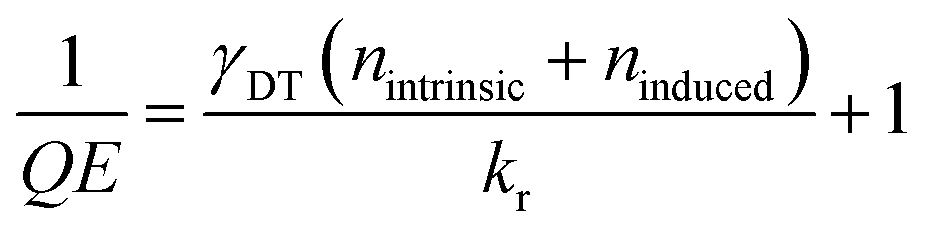 | (4) |
We assume QE = 1 in the absence of sulfur vacancies, the dominant nonradiative centers in our system. Based on the linear fit in Fig. 2(a), the intrinsic defect density is estimated to be nintrinsic ≈ 6 × 1012 cm−2, indicating a substantial background of native sulfur vacancies in the pristine sample. Using a reported radiative recombination rate of kr ≈ 0.1 ns−1 from time-resolved PL measurements (tr-PL) on MOCVD-grown WS2,8,40 we extract a trapping coefficient of γDT ≈ 3 × 10⁻¹³ cm2 ps−1.
This steady-state model forms the basis for comparison with time-resolved measurements, where the interplay between DT and EEA will be examined in detail. Beyond quantifying the intrinsic defect density, the QE analysis also provides insight into the spatial distribution of trapping centers. When plotted against the average defect distance, including intrinsic contributions, the data suggest a relatively uniform defect distribution across the irradiated samples (Fig. 2(b)). However, the analysis of DT rate relies on radiative lifetime values derived from tr-PL, which are limited by their temporal resolution. To obtain a more accurate and dynamic picture of defect-mediated exciton decay, we turn to femtosecond transient absorption (TA) spectroscopy in the following section.
2.2 Time-resolved measurements
Time-resolved experiments were conducted as illustrated schematically in Fig. 3(a). Two excitation wavelengths were employed to access distinct electronic transitions. A 400 nm (3.1 eV) pump predominantly excites the high-energy C exciton region, followed by ultrafast relaxation into A and B exciton states within tens of femtoseconds.41 The A and B excitons are hallmark features of TMDC monolayers, arising from spin–orbit splitting of the valence band. Both are spin-singlet states, differing only in the relative spin alignment of the electron and hole.42 To probe defect-related transitions, additional measurements were performed using sub-bandgap excitation at 700 nm (1.77 eV), targeting in-gap states associated with sulfur vacancies. | ||
| Fig. 3 (a) Schematic illustration of exciton dynamics in WS2 in the presence of defect states. Under 400 nm excitation, carriers are excited from the valence band to the conduction band near the C exciton region, while 700 nm excitation drives transitions from occupied in-gap defect states to the conduction band. To aid visualization, the 700 nm excitation is depicted as shifted away from the K point in momentum space. Generated excitons (after ultrafast relaxation) can decay nonradiatively via defect trapping (DT) or exciton–exciton annihilation (EEA). With sufficient photon absorption, carriers can also be excited to higher energy states through excited state absorption (ESA). The band structure, including defect states of a simply charged sulfur vacancy, is shown based on DFT calculations. (b) Colourmaps of the TA spectra for samples with the lowest (left) and highest (right) defect densities. The signals are normalized to their respective minimum signals and plotted as a function of probe energy (eV) and pump–probe delay time (ps). | ||
Colourmaps of the TA spectra for samples with the lowest and highest defect densities are shown in Fig. 3(b), normalized to their respective minimum signals. The estimated intrinsic sulfur vacancy densities, derived from steady-state analysis, are included for reference. A tailored temporal sampling scheme was employed, using finer steps (down to 50 fs) during the initial picoseconds to capture ultrafast dynamics, and coarser steps at longer delays. Colourmaps for the other two samples are provided in Fig. S2, along with spectral cuts at a delay of 2 ps for all samples.
At this timescale, distinct Pauli blocking features appear at ≈2.05 eV and above 2.4 eV, corresponding to the A- and B-exciton transitions, respectively. These features reflect a reduction in absorption due to state filling by photoexcited excitons.43 In addition to Pauli blocking, two positive signal features emerge in the TA spectra. These are attributed to photoinduced excited-state absorption (ESA), in which carriers in the conduction band absorb probe photons to access higher-lying electronic states,43 and to photo-induced band renormalization, leading to a spectral shift between pump-off and pump-on conditions.44
In the following, we focus on the A-exciton Pauli blocking region to track exciton dynamics as a function of defect density. For consistency, all analyses are based on the absolute value of the differential signal.
2.3 Evidence for occupied in-gap states
We begin our analysis by examining the signal amplitude at t = 0 ps. The absolute A-exciton signal intensity under 400 nm and 700 nm excitation was extracted via Gaussian fitting (see Fig. S3) and normalized to the value of the lowest-defect-density sample (Fig. 4(a)). Under 400 nm excitation, a slight decrease in peak intensity is observed with increasing defect density, while sub-bandgap excitation at 700 nm yields a pronounced increase. | ||
| Fig. 4 (a) Comparison of A-exciton peak intensities at 0 ps extracted from Gaussian fitting under 400 nm (purple) and 700 nm (red) pump excitation for different defect densities. Intensities are normalized to the least defective sample for both excitation conditions. A slight decrease in intensity with increasing defect density is observed under 400 nm excitation, while 700 nm excitation shows a pronounced increase. The dashed line is solely a visual guide. (b) A-exciton peak intensity as a function of pump fluence under 700 nm excitation, plotted on a log–log scale. The fitted slope of 0.77 indicates that the excitation mechanism is not dominated by two-photon absorption. Error bars in both panels represent uncertainties from Gaussian fitting. | ||
For 400 nm excitation, carriers are initially excited into higher-energy states and subsequently relax into the A-exciton manifold.41 At higher defect densities, carriers can be increasingly captured by in-gap states before reaching the A-exciton state, resulting in a slightly reduced signal intensity. In contrast, excitation at 700 nm (below the bandgap) is expected to drive transitions from occupied in-gap states into the conduction band. The observed intensity increase with defect density suggests a rising population of such occupied states.
To rule out two-photon absorption as the origin of this signal, we performed fluence-dependent measurements (Fig. 4(b)). The resulting log–log plot exhibits a linear dependence with a slope of 0.77, well below the expected value of 2 for a two-photon process.45 This confirms that the excitation originates from one-photon transitions involving occupied in-gap defect states. While such excitation may also generate free carriers that contribute to trion formation, their concentration appears limited. This is evidenced by the substantially lower overall signal amplitude under 700 nm excitation compared to 400 nm, despite the use of significantly higher pump fluence.
These findings are initially surprising, as neutral sulfur vacancies are not expected to introduce occupied in-gap states. To explore this discrepancy, we performed density functional theory (DFT) calculations to assess the electronic structure of charged sulfur vacancies (Fig. S4 and S5). The charge transition level (CTL) from neutral to singly charged VS− lies at an acceptor level just below the conduction band. Both singly and doubly negatively charged VS configurations exhibit multiple occupied in-gap states, consistent with our spectroscopic observations. Experimentally, such negatively charged vacancies have been identified via scanning tunneling microscopy (STM), where characteristic contrast was attributed to chalcogen vacancies in distinct charge states.38
Defect-induced modifications to the exciton transition energy also become evident when tracking the A-exciton peak position. At t = 0 ps, a systematic blueshift is observed with increasing defect density (Fig. S6), in agreement with the PL trend in Fig. 1(c). In addition, a transient blueshift of the exciton resonance is observed over time, attributed to the relaxation of the band structure back to its equilibrium configuration after photoexcitation.44 Notably, this relaxation occurs more rapidly in samples with higher defect densities (Fig. S7), suggesting faster carrier localization in the presence of defect states.
2.4 Exciton dynamics under strong photoexcitation
Following the analysis at t = 0 ps, we turn to the time-resolved evolution of the A-exciton signal. A temporal blueshift of the peak energy is observed across all samples, necessitating dynamic spectral corrections at each delay step. To accurately extract decay kinetics, a time-dependent fitting procedure was employed: a spectral window was adaptively centred on the A-exciton resonance, and the peak was modeled using asymmetric Gaussian functions to determine both position and amplitude (Fig. S3). The resulting normalized intensity traces are plotted on a logarithmic scale in Fig. 5(a). A clear trend emerges: higher defect densities yield faster exciton decay. As discussed in the steady-state analysis, two ultrafast nonradiative channels dominate: EEA and DT, schematically illustrated in Fig. 3(a). Notably, EEA is activated only at sufficiently high initial exciton densities. To assess this, the initial exciton density n(0) for each sample was estimated using the relation:46 | (5) |
 | ||
| Fig. 5 (a) Normalized, shift-corrected A-exciton decay traces of samples with varying defect densities up to 5 ps (left). Representative A-exciton decay fits from 0.3 to 50 ps for the sample with the highest induced defect density (right). Both panels are plotted on a logarithmic scale. The corresponding fitting residuals, defined as the difference between the raw and fitted data, are plotted as a function of delay time (ps). The small amplitude of these residuals, remaining within ± 0.01, indicates good fit quality. (b) γEEAn(0) as a function of defect density, extracted from different fitting time windows. Error bars indicate deviations across fitting windows. (c) knrA extracted from different fitting time windows as a function of defect density. A linear trend is observed, with the grey shaded area representing the range of linear fits obtained from different fitting windows. Black dots indicate the average knrA values. The red line corresponds to a trace replotted using the average γDT and k′ values from all linear fits. | ||
Here, F denotes the pump fluence (J cm−2), α the absorbance at the pump wavelength (unitless), ħν the photon energy, and Φ the exciton generation efficiency. Assuming an exciton generation yield of unity and an absorbance of 0.06 at 400 nm for the monolayer MOCVD-grown WS2 sample,43,47 the initial exciton density is estimated to be 1.606 × 1013 cm−2 for a pump fluence of 0.133 mJ cm−2. Despite this high density, no signs of exciton generation saturation are observed (Fig. S8).
Given the high n(0), EEA must be considered alongside DT in the decay kinetics. To account for both pathways, we apply a rate equation model that includes EEA, DT, and radiative recombination as parallel, competing channels:48,49
 | (6) |
As previously discussed, the quantum efficiency is low (≈3.2 × 10⁻⁵) for the pristine sample, justifying the omission of the radiative recombination term in the decay model. EEA is treated as a second-order Auger-type process, in which one exciton recombines nonradiatively by transferring its energy to a second exciton, promoting it to a higher-energy state (Fig. 3(a)).48,50 In contrast, DT is modelled as a first-order process governed by the defect density and contributes to the effective nonradiative rate constant knr, alongside other ultrafast decay pathways, which will be discussed in detail later. The competing nature of these channels motivates the following kinetic model:
 | (7) |
Eqn (7) captures the exciton decay dynamics using two distinct time-dependent components. The first term, scaled by amplitude A, is derived from the solution of a model considering the EEA channel,48 with effective nonradiative decay rate knrA. The parameter γEEA is the EEA rate coefficient. The second term, weighted with amplitude B, accounts for slower, first-order nonradiative processes, such as exciton diffusion to grain boundaries.51 This dominates at later times when EEA becomes negligible, with rate constant knrB. The separation of the two terms suggests that EEA is active only within the first few picoseconds. The constant C accounts for a long-lived signal offset outside the experimental detection window.
Prior to decay fitting, the instrument response function (IRF) was determined from the leading edge of the signal, including the negative delay region, yielding σIRF ≈ 65 fs. This is comparable to the pump pulse duration, with a full width at half maximum (FWHM) ≈ 100–150 fs (Fig. S9). To avoid influence from the initial rise, the fit range was restricted to times t ≥ 0.3 ps, with the upper limit varied between 25 and 50 ps in 0.5 ps steps to assess sensitivity to the fitting window. Fig. 5(a) shows an example for the sample with the highest defect density. The extracted values for γEEAn(0) and knrA vary systematically with defect density (Fig. 5(b and c)). Error bars in grey represent the spread of values across the different fitting windows, illustrating the sensitivity of the extracted parameters to the chosen temporal range.
Starting from the EEA component, we extract the annihilation rate coefficient γEEA using the estimated initial exciton density n(0) = 1.606 × 1013 cm−2. This yields γEEA values ranging from approximately 0.05 to 0.14 cm2 s−1, in good agreement with previous reports.4,8,50,52,53 Notably, γEEAn(0) becomes difficult to extract from the fitting (approaches zero) at the highest defect density (Fig. 5(b)). This suggests a critical threshold in the defect-to-exciton ratio of ≈ 3.5, below which two excitons can still interact before encountering a defect, whereas above this value, DT dominates the decay dynamics.
For knrA, a similar assumption to that used in the steady-state PL analysis (eqn (2) and (3)) is applied. However, unlike in PL, the high initial exciton densities in TA experiments can lead to partial saturation of defect states, since their recovery upon occupation occurs on nanosecond timescales.12 As a result, excess excitons may decay via alternative nonradiative channels. These additional pathways can be ultrafast, such as k′, which may involve trapping at intrinsic defect species not modified by irradiation. Moreover, carrier–phonon scattering may contribute,43,54,55 particularly under strong excitation. Rapid relaxation of high-energy excitons generates a significant phonon population, which may subsequently scatter with excitons at the bandedge.
The contribution of additional ultrafast channels, denoted as k′, can be extracted by analyzing the linear dependence of knrA on defect density. The corresponding fit results are shown in Fig. 5(c), with shaded regions representing variations due to the choice of fitting window. A representative linear fit (red line) is plotted using the average values of k′ ≈ 0.55 ps−1 and γDT = 2.15 × 10⁻¹⁴ cm2 ps−1. Notably, when comparing the γDT values obtained from steady-state and time-resolved measurements—3.0 × 10⁻¹³ cm2 ps−1vs. 2.15 × 10⁻¹⁴ cm2 ps−1, respectively—a clear discrepancy of more than an order of magnitude emerges. This result suggests that at high initial exciton densities, excitons may either undergo annihilation before reaching a defect site or encounter a defect that is already occupied by a previously trapped exciton, thereby preventing further nonradiative recombination on ultrafast timescales. Consequently, the effective defect trapping rate per unit defect decreases with increasing exciton density. In line with this, the extracted kDT from time-resolved measurements is significantly lower than the steady-state value, supporting our assumption that k′ can be neglected in steady-state analyses but should be retained in the TA model.
2.5 Diffusion-limited competition
To further examine the interplay between EEA and DT, we consider that both processes are governed by diffusion-limited kinetics. In the case of EEA, excitons undergo random diffusion until they encounter another exciton within a characteristic annihilation radius REEA, leading to immediate recombination.56 According to Smoluchowski's theory, γEEA is proportional to the exciton diffusion coefficient D for LD ≫ REEA, where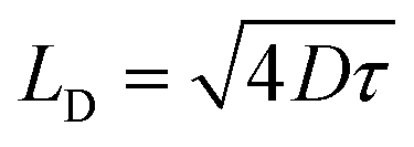 denotes the exciton diffusion length56–59 and τ is the effective exciton lifetime. We propose a simplified model in which DT follows an analogous mechanism: an exciton is captured once it diffuses within a trapping radius RDT of a defect.
To illustrate the diffusion-limited character of both decay pathways, we compare representative exciton lifetimes and diffusion lengths under EEA- and DT-dominated conditions. For simplicity, we incorporate the additional nonradiative term k′ into the DT channel, treating it as one single competing channel to EEA. We begin with a scenario where both the initial exciton density and the defect density are approximately 1.6 × 1013 cm−2, corresponding to an average spacing of ≈2.5 nm between excitons or defects. Under EEA-limited conditions, the effective exciton lifetime is 0.7 ps, while in the DT-limited case, it is 1.3 ps. Assuming a diffusion coefficient of D = 0.3 cm2 s−1,60 this yields diffusion lengths of ≃9 nm (EEA) and ≃13 nm (DT), respectively.
Given that both estimates refer to the same average spatial separation, the comparable diffusion lengths suggest that the effective annihilation and trapping radii are of similar magnitude. At the highest defect density, where the exciton lifetime shortens to 0.6 ps, the diffusion length falls below that of the EEA regime. This indicates that DT becomes the dominant process, effectively suppressing the EEA channel. Consistent with this interpretation, the extracted value of γEEAn(0) approaches zero in the most defective sample.
2.6 Conclusions
In this work, we quantitatively investigated exciton decay pathways in wafer-scale MOCVD-grown monolayer WS2 by combining steady-state quantum efficiency measurements and femtosecond transient absorption spectroscopy. Controlled defect introduction enabled the estimation of intrinsic sulfur vacancy densities and unit defect trapping rates. Time-resolved measurements provided strong evidence for occupied in-gap defect states and reveal a competition between exciton–exciton annihilation and defect trapping that depends on both excitation conditions and defect concentrations.A critical defect-to-exciton ratio (≈3.5) was identified as the threshold for activating EEA, beyond which DT dominates due to shorter exciton diffusion lengths. Under high exciton densities, partial defect saturation reduces trapping efficiency, further modulating the recombination landscape.
These findings establish a quantitative framework for diffusion-limited exciton dynamics, providing critical guidance for future defect engineering strategies aimed at enhancing the functionality of device applications based on large-area two-dimensional TMDCs.
3 Materials and methods
3.1 MOCVD growth
The MOCVD WS2 sample was synthesized in a commercial AIXTRON CCS multi-wafer MOCVD reactor. Tungsten hexacarbonyl (W(CO)6) and ditert-butyl sulfide (DTBS) were used as precursors. H2 was chosen as carrier gas. The deposition of WS2 includes two stages: the nucleation process (stage I) at 750 °C for 10 min and lateral growth (stage II) at 800 °C for 95 min with reduced W(CO)6 flux. The substrate is double-side polished c-plane sapphire with a 0.2° off-cut towards the m-plane.3.2 Ion bombardment
For defect creation, the ion sputtering gun model IG35/IG70 from OCI Vacuum Microengineering Inc. was used. Argon gas with 99.999% purity from Air Liquide was filled into the chamber until a pressure 5 × 10⁻⁶ mbar was reached. The current density was set to 0.088 µA cm−2 corresponding to an ion flux of 5.5 × 10¹¹ ions per cm2 s. The samples were exposed to the ion beam until the targeted fluence was reached.3.3 SEM
SEM measurements were performed with a Zeiss Sigma HV, with a voltage of 10 kV, at a working distance of 2.6 mm, an aperture of 20 µm and under a stage tilt of 0.4°, enabling a magnification of 60![[thin space (1/6-em)]](https://www.rsc.org/images/entities/char_2009.gif) 000.
000.
3.4 PL and Raman spectroscopy
All PL and Raman measurements were performed with a Witec Alpha300 R setup, using a 532 nm cw laser. The laser spot diameter is estimated to be around 590 nm, which results in a laser power of 0.36 kW cm−2. The exciton formation rate is estimated to be approximately 7 × 10¹⁰ ps−1 cm−2.3.5 QE determination
To determine the QE, the relative determination method was used. CdSe quantum dots spin-coated onto a sapphire substrate were used as a reference sample. The internal quantum efficiency of the reference sample was determined by an integrating sphere method and was obtained as 66%. Further, the absorption of the MOCVD sample and the reference sample at 532 nm excitation wavelength was measured as 7% and 8% respectively, enabling the determination of the QE through PL measurements.3.6 Transient absorption spectroscopy
Femtosecond broadband transient absorption measurements were performed using a pump–probe system driven by a Pharos-SP laser (Light Conversion). The laser delivers fundamental pulses with a central wavelength of 1030 nm, a pulse duration of 170 fs, and an energy of 1 mJ, operating at a 6 kHz repetition rate. The pump pulses were generated using an optical parametric amplifier (Orpheus) with a second harmonic generation (SHG) module. Under 400 nm and 700 nm pumps, the samples were excited with fluences of 0.133 mJ cm−2 and 2.541 mJ cm−2. The probe beam consisted of a white-light supercontinuum, produced by focusing a small fraction of the fundamental beam onto a YAG crystal, yielding a probed wavelength range of 500–950 nm (corresponding to an energy range of 1.3–2.4 eV). The pump and probe spot sizes are 250 µm and 80 µm, respectively. They are linearly polarized and oriented perpendicular to each other. The arrival time of the probe pulses relative to the pump pulses was precisely controlled using an optical delay stage. Multiple scans were run and averaged for data analysis, and to rule out any alteration of the sample through the lasers, each scan in a row was checked for changes.3.7 DFT calculations
First-principles calculations were performed using density functional theory (DFT) with VASP 6.3.0 version package.61,62 The interactions between ions and valence electrons were described using the projector-augmented wave (PAW)63 method, and electronic exchange and correlation were treated by the generalized gradient approximation of Perdew, Burke, and Ernzerhof (PBE).64 We employed a plane wave cut-off energy of 500 eV. The material models, including the defective system, were built in a 6 × 6 × 1 supercell with 15 Å vacuum to avoid interaction with the periodic images, which corresponds to a defect density of 2.1 × 1013 cm−2. A 9 × 9 × 1 Monkhorst–Pack k-point grid was used to sample the 2D Brillouin zone.Author contributions
R. Z., L. D., G. S., and M. S. jointly conceived the idea of the study. R. Z., under the supervision of G. S., and L. D., under the supervision of M. S., co-wrote the main content of the manuscript and contributed equally to the work. R. Z. performed the transient absorption measurements and contributed to data analysis and discussion. L. D. prepared the samples, conducted ion bombardment, performed Raman and steady-state quantum efficiency measurements and contributed to data analysis and discussion. D. S., supervised by P. K., performed the density functional theory (DFT) calculations and participated in the discussion. C. V., under the supervision of G. S., assisted with TA data analysis and contributed to the discussion. Y. D., under the supervision of A. V. and H. K., provided the pristine MOCVD-grown samples and performed scanning electron microscopy (SEM) measurements. M. H. from Aixtron SE contributed to the coordination of the sample preparation project using a commercial MOCVD tool. T. F., under the supervision of G. B., performed quantum efficiency measurements on the pristine MOCVD samples. All authors contributed to the interpretation of the results and to the preparation of the manuscript. G. S. and M. S. supervised the overall project.Conflicts of interest
The authors declare no conflict of interest.Data availability
The data supporting this article have been included as part of the supplementary information (SI) and are available via the University of Waterloo Dataverse (Borealis) at https://doi.org/10.5683/SP3/ZDPLRA. Supplementary information: trion and exciton fitting of photoluminescence spectra; colourmaps of transient absorption spectra for other samples; asymmetric Gaussian fitting of the A-exciton peak; simulated STM and electronic structure of charged sulfur vacancies; defect-dependent shifts of the A-exciton peak under 400 nm and 700 nm excitation; time-resolved blue shifts and fitting of their rate constants; analysis of exciton generation saturation at high pump fluence; and instrument response function analysis of ultrafast exciton dynamics. See DOI: https://doi.org/10.1039/d5sc07343j.Acknowledgements
The authors gratefully acknowledge funding support from the Natural Sciences and EngineeringResearch Council of Canada (NSERC) [CREATE 565360] and the Deutsche Forschungsgemeinschaft (DFG, German Research Foundation) [IRTG 2803-461605777]. They also acknowledge the funding support from the Canada Foundation for Innovation and the Ontario Research Fund, and the support provided by Compute Canada and the Digital Research Alliance of Canada (alliancecan.ca). R. Z. and C. V. acknowledge funding support from the Mitacs Globalink Research Award program. Further funding from the DFG is acknowledged under project numbers 278162697 (CRC 1242 “Non-Equilibrium Dynamics of Condensed Matter in the Time Domain”) and 429784087. The authors also acknowledge computing time granted by the Center for Computational Sciences and Simulation (CCSS) at the University of Duisburg-Essen, provided on the supercomputer magnitUDE (DFG Grant No. INST 20876/209-1 FUGG and INST 20876/243-1 FUGG) at the Zentrum für Informations-und Mediendienste (ZIM).Notes and references
- K. F. Mak, C. Lee, J. Hone, J. Shan and T. F. Heinz, Phys. Rev. Lett., 2010, 105, 136805 CrossRef.
- H. R. Gutiérrez, N. Perea-López, A. L. Elías, A. Berkdemir, B. Wang, R. Lv, F. López-Urías, V. H. Crespi, H. Terrones and M. Terrones, Nano Lett., 2013, 13, 3447–3454 CrossRef PubMed.
- X. Xin, Y. Zhang, J. Chen, M.-L. Chen, W. Xin, M. Ding, Y. Bao, W. Liu, H. Xu and Y. Liu, Mater. Horiz., 2022, 9, 2416–2424 RSC.
- Y. Lee, J. D. S. Forte, A. Chaves, A. Kumar, T. T. Tran, Y. Kim, S. Roy, T. Taniguchi, K. Watanabe, A. Chernikov, J. I. Jang, T. Low and J. Kim, Nat. Commun., 2021, 12, 7095 CrossRef CAS.
- H. Kim, S. Z. Uddin, N. Higashitarumizu, E. Rabani and A. Javey, Science, 2021, 373, 448–452 CrossRef CAS PubMed.
- D. Andrzejewski, R. Oliver, Y. Beckmann, A. Grundmann, M. Heuken, H. Kalisch, A. Vescan, T. Kümmell and G. Bacher, Adv. Opt. Mater., 2020, 8, 2000694 CrossRef CAS.
- U. Hutten, L. Daniel, A. Grundmann, N. Stracke, M. Abdelbaky, Y. Beckmann, M. Heuken, W. Mertin, H. Kalisch, A. Vescan, G. Bacher and T. Kümmell, 2D Mater., 2021, 8, 045015 CrossRef CAS.
- L. Yuan and L. Huang, Nanoscale, 2015, 7, 7402–7408 RSC.
- D. Sun, Y. Rao, G. A. Reider, G. Chen, Y. You, L. Brézin, A. R. Harutyunyan and T. F. Heinz, Nano Lett., 2014, 14, 5625–5629 CrossRef CAS PubMed.
- L. Yin, P. He, R. Cheng, F. Wang, F. Wang, Z. Wang, Y. Wen and J. He, Nat. Commun., 2019, 10, 4133 CrossRef PubMed.
- C. Kastl, R. J. Koch, C. T. Chen, J. Eichhorn, S. Ulstrup, A. Bostwick, C. Jozwiak, T. R. Kuykendall, N. J. Borys, F. M. Toma, S. Aloni, A. Weber-Bargioni, E. Rotenberg and A. M. Schwartzberg, ACS Nano, 2019, 13, 1284–1291 CAS.
- L. Li and E. A. Carter, J. Am. Chem. Soc., 2019, 141, 10451–10461 CrossRef CAS.
- M. Chubarov, T. H. Choudhury, D. R. Hickey, S. Bachu, T. Zhang, A. Sebastian, A. Bansal, H. Zhu, N. Trainor, S. Das, M. Terrones, N. Alem and J. M. Redwing, ACS Nano, 2021, 15, 2532–2541 CrossRef CAS PubMed.
- Y. Wan, E. Li, Z. Yu, J.-K. Huang, M.-Y. Li, A.-S. Chou, Y.-T. Lee, C.-J. Lee, H.-C. Hsu, Q. Zhan, A. Aljarb, J.-H. Fu, S.-P. Chiu, X. Wang, J.-J. Lin, Y.-P. Chiu, W.-H. Chang, H. Wang, Y. Shi, N. Lin, Y. Cheng, V. Tung and L.-J. Li, Nat. Commun., 2022, 13, 4149 CrossRef CAS PubMed.
- E. Pollmann, L. Madauß, S. Schumacher, U. Kumar, F. Heuvel, C. vom Ende, S. Yilmaz, S. Güngörmüs and M. Schleberger, Nanotechnology, 2020, 31, 505604 CrossRef CAS.
- Y.-H. Wang, H.-M. Ho, X.-L. Ho, L.-S. Lu, S.-H. Hsieh, S.-D. Huang, H.-C. Chiu, C.-H. Chen, W.-H. Chang, J. D. White, Y.-H. Tang and W.-Y. Woon, ACS Appl. Nano Mater., 2021, 4, 11693–11699 CrossRef CAS.
- M. G. Bianchi, F. Risplendi, M. Re Fiorentin and G. Cicero, Adv. Sci., 2024, 11, e2305162 CrossRef PubMed.
- S. Sleziona, O. Kharsah, L. Skopinski, L. Daniel, J. Schmeink and M. Schleberger, Adv. Electron. Mater., 2024, 2400318 Search PubMed.
- S. Sleziona, A. Pelella, E. Faella, O. Kharsah, L. Skopinski, A. Maas, Y. Liebsch, J. Schmeink, A. D. Bartolomeo and M. Schleberger, Nanoscale Adv., 2019, 5, 6958 RSC.
- A. Pelella, O. Kharsah, A. Grillo, F. Urban, M. Passacantando, F. Giubileo, L. Iemmo, S. Sleziona, E. Pollmann, L. Madauß, M. Schleberger and A. Di Bartolomeo, ACS Appl. Mater. Interfaces, 2020, 12, 40532–40540 CrossRef CAS.
- L. Madauß, O. Ochedowski, H. Lebius, B. Ban-d’Etat, C. Naylor, A. Johnson, J. Kotakoski and M. Schleberger, 2D Mater., 2017, 4, 015034 CrossRef.
- M. Schleberger and J. Kotakoski, Materials, 2018, 11, 1885 CrossRef PubMed.
- A. Asaithambi, R. Kozubek, G. M. Prinz, F. Reale, E. Pollmann, M. Ney, C. Mattevi, M. Schleberger and A. Lorke, Phys. Status Solidi RRL, 2021, 15, 2000466 CrossRef CAS.
- D.-H. Lien, S. Z. Uddin, M. Yeh, M. Amani, H. Kim, J. W. Ager, E. Yablonovitch and A. Javey, Science, 2019, 364, 468–471 CrossRef CAS PubMed.
- M. Amani, D.-H. Lien, D. Kiriya, J. Xiao, A. Azcatl, J. Noh, S. R. Madhvapathy, R. Addou, S. KC, M. Dubey, K. Cho, R. M. Wallace, S.-C. Lee, J.-H. He, J. W. Ager, X. Zhang, E. Yablonovitch and A. Javey, Science, 2015, 350, 1065–1068 CrossRef CAS.
- H. Lu, A. Kummel and J. Robertson, APL Mater., 2018, 6, 066104 CrossRef.
- W. Zhao, Z. Ghorannevis, K. K. Amara, J. R. Pang, M. Toh, X. Zhang, C. Kloc, P. H. Tan and G. Eda, Nanoscale, 2013, 5, 9677–9683 RSC.
- A. Berkdemir, H. R. Gutiérrez, A. R. Botello-Méndez, N. Perea-López, A. L. Elías, C.-I. Chia, B. Wang, V. H. Crespi, F. López-Urías, J.-C. Charlier, H. Terrones and M. Terrones, Sci. Rep., 2013, 3, 1–8 Search PubMed.
- M. Staiger, R. Gillen, N. Scheuschner, O. Ochedowski, F. Kampmann, M. Schleberger, C. Thomsen and J. Maultzsch, Phys. Rev. B, 2015, 91, 195419 CrossRef.
- J. W. Christopher, B. B. Goldberg and A. K. Swan, Sci. Rep., 2017, 7, 14062 CrossRef PubMed.
- J. Mo, S. El Kazzi, W. Mortelmans, A. N. Mehta, S. Sergeant, Q. Smets, I. Asselberghs and C. Huyghebaert, Nanotechnology, 2020, 31, 125604 CrossRef CAS PubMed.
- L. Ma, Y. Tan, M. Ghorbani-Asl, R. Boettger, S. Kretschmer, S. Zhou, Z. Huang, A. V. Krasheninnikov and F. Chen, Nanoscale, 2017, 9, 11027–11034 RSC.
- J. F. Ziegler, M. D. Ziegler and J. P. Biersack, Nucl. Instrum. Methods Phys. Res., Sect. B, 2010, 268, 1818–1823 CrossRef CAS.
- H. Liu, C. Wang, Z. Zuo, D. Liu and J. Luo, Adv. Mater., 2020, 32, e1906540 CrossRef.
- W. Lu, B. Birmingham and Z. Zhang, Appl. Surf. Sci., 2020, 532, 147461 CrossRef CAS.
- S. Bertolazzi, S. Bonacchi, G. Nan, A. Pershin, D. Beljonne and P. Samorì, Adv. Mater., 2017, 29, 1606760 CrossRef PubMed.
- T. Y. Jeong, H. Kim, S.-J. Choi, K. Watanabe, T. Taniguchi, K. J. Yee, Y.-S. Kim and S. Jung, Nat. Commun., 2019, 10, 3825 CrossRef PubMed.
- B. Schuler, D. Y. Qiu, S. Refaely-Abramson, C. Kastl, C. T. Chen, S. Barja, R. J. Koch, D. F. Ogletree, S. Aloni, A. M. Schwartzberg, J. B. Neaton, S. G. Louie and A. Weber-Bargioni, Phys. Rev. Lett., 2019, 123, 076801 CrossRef CAS.
- H. Liu, C. Wang, D. Liu and J. Luo, Nanoscale, 2019, 11, 7913–7920 RSC.
- A. Cohen, A. Patsha, P. K. Mohapatra, M. Kazes, K. Ranganathan, L. Houben, D. Oron and A. Ismach, ACS Nano, 2021, 15, 526–538 CrossRef CAS PubMed.
- C. Trovatello, F. Katsch, N. J. Borys, M. Selig, K. Yao, R. Borrego-Varillas, F. Scotognella, I. Kriegel, A. Yan, A. Zettl, P. J. Schuck, A. Knorr, G. Cerullo and S. D. Conte, Nat. Commun., 2020, 11, 5277 CrossRef CAS.
- B. Zhu, X. Chen and X. Cui, Sci. Rep., 2015, 5, 9218 CrossRef PubMed.
- Y. Li, X. Wu, W. Liu, H. Xu and X. Liu, Appl. Phys. Lett., 2021, 119, 051106 CrossRef CAS.
- E. A. A. Pogna, M. Marsili, D. De Fazio, S. Dal Conte, C. Manzoni, D. Sangalli, D. Yoon, A. Lombardo, A. C. Ferrari, A. Marini, G. Cerullo and D. Prezzi, ACS Nano, 2016, 10, 1182–1188 CrossRef CAS.
- N. V. Tkachenko, Optical Spectroscopy : Methods and Instrumentations, Elsevier, Amsterdam, 1st edn, 2006, p. 293 Search PubMed.
- A. Chernikov, C. Ruppert, H. M. Hill, A. F. Rigosi and T. F. Heinz, Nat. Photonics, 2015, 9, 466–470 CrossRef CAS.
- T. Zhang and J. Wang, ACS Photonics, 2021, 8, 2770–2780 CrossRef CAS.
- Y.-Z. Ma, L. Valkunas, S. L. Dexheimer, S. M. Bachilo and G. R. Fleming, Phys. Rev. Lett., 2005, 94, 1574021–1574024 CrossRef PubMed.
- C. Robert, D. Lagarde, F. Cadiz, G. Wang, B. Lassagne, T. Amand, A. Balocchi, P. Renucci, S. Tongay, B. Urbaszek and X. Marie, Phys. Rev. B, 2016, 93, 205423 CrossRef.
- N. Kumar, Q. Cui, F. Ceballos, D. He, Y. Wang and H. Zhao, Phys. Rev. B, 2014, 89, 125427 CrossRef.
- M. Yang, Y. Zeng, Z. Li, D. H. Kim, C.-S. Jiang, J. van de Lagemaat and K. Zhu, Phys. Chem. Chem. Phys., 2017, 19, 5043–5050 RSC.
- L. Sortino, M. Gülmüs, B. Tilmann, L. de S Menezes and S. A. Maier, Light Sci. Appl., 2023, 12, 202 CrossRef CAS.
- Y. Yu, Y. Yu, C. Xu, A. Barrette, K. Gundogdu and L. Cao, Phys. Rev. B, 2016, 93, 201111 CrossRef.
- H. Shi, R. Yan, S. Bertolazzi, J. Brivio, B. Gao, A. Kis, D. Jena, H. G. Xing and L. Huang, ACS Nano, 2013, 7, 1072–1080 CrossRef CAS PubMed.
- J. Shi, Y. Li, Z. Zhang, W. Feng, Q. Wang, S. Ren, J. Zhang, W. Du, X. Wu, X. Sui, Y. Mi, R. Wang, Y. Sun, L. Zhang, X. Qiu, J. Lu, C. Shen, Y. Zhang, Q. Zhang and X. Liu, ACS Photonics, 2019, 6, 3082–3091 CrossRef CAS.
- S. Kumar, I. S. Dunn, S. Deng, T. Zhu, Q. Zhao, O. F. Williams, R. Tempelaar and L. Huang, Nat. Chem., 2023, 15, 1118–1126 CrossRef CAS.
- M. v. Smoluchowski, Z. Phys. Chem., 1918, 92U, 129–168 CrossRef.
- A. Suna, Phys. Rev. B, 1970, 1, 1716–1739 CrossRef.
- A. J. Goodman, D.-H. Lien, G. H. Ahn, L. L. Spiegel, M. Amani, A. P. Willard, A. Javey and W. A. Tisdale, J. Phys. Chem. C, 2020, 124, 12175–12184 CrossRef CAS.
- M. Kulig, J. Zipfel, P. Nagler, S. Blanter, C. Schüller, T. Korn, N. Paradiso, M. M. Glazov and A. Chernikov, Phys. Rev. Lett., 2018, 120, 207401 CrossRef CAS.
- G. Kresse and J. Furthmüller, Phys. Rev. B, 1996, 54, 11169–11186 CrossRef CAS.
- G. Kresse and D. Joubert, Phys. Rev. B, 1999, 59, 1758–1775 CrossRef CAS.
- P. E. Blöchl, Phys. Rev. B, 1994, 50, 17953–17979 CrossRef.
- J. P. Perdew, K. Burke and M. Ernzerhof, Phys. Rev. Lett., 1996, 77, 3865–3868 CrossRef CAS.
Footnote |
| † These authors contributed equally. |
| This journal is © The Royal Society of Chemistry 2026 |