DOI:
10.1039/D6RA01845A
(Paper)
RSC Adv., 2026,
16, 24378-24399
Theoretical study of GaBX3 halide perovskites for optoelectronic and energy conversion applications
Received
3rd March 2026
, Accepted 4th May 2026
First published on 11th May 2026
Abstract
ABX3 perovskite materials have shown great potential for optoelectronic applications in recent years. In this study, first-principles density functional theory (DFT) is used to thoroughly analyze the structural, electronic, thermo-mechanical and photocatalytic properties of lead-free novel cubic halide perovskites GaBX3 (B = Cd, Zn; X = Cl, Br). Structural analysis brought about the thermodynamic stability in the space group Pm![[3 with combining macron]](https://www.rsc.org/images/entities/char_0033_0304.gif) m with negative formation enthalpy and decomposition energy. GaZnCl3 was found to have the most stable material with a formation enthalpy of −2.938 eV per atom. Negative decomposition energies confirm the stability of these ternary phases against separation into binary constituents. Electronic band structure calculations, refined with the HSE06 functional, show that the bandgap of these novel materials varies from 0.65–3.37 eV. The optical properties are high absorption coefficients more than 105 cm−1 in the UV and visible regions, as well as a static refractive index between 1.85 and 2.20 increasing with Br substituent. The ductile nature (B/G > 1.75) and satisfying Born Stability Criteria proves mechanical stability. Thermal property analysis, including Debye temperatures up to 240 K, suggests high lattice rigidity and stability in Cl-based systems. Furthermore, the band edge alignments demonstrate that these materials possess the requisite redox potentials for visible light driven water splitting, with valence band maxima (VBM) and conduction band minima (CBM) effectively straddling the water oxidation and reduction potentials. While phonon dispersion curves at 0 K exhibit imaginary frequencies, indicating the cubic phase as a metastable state stabilized by finite-temperature effects. These findings strongly suggest the prospective applications of these novel materials in a wide range of optoelectronic devices.
m with negative formation enthalpy and decomposition energy. GaZnCl3 was found to have the most stable material with a formation enthalpy of −2.938 eV per atom. Negative decomposition energies confirm the stability of these ternary phases against separation into binary constituents. Electronic band structure calculations, refined with the HSE06 functional, show that the bandgap of these novel materials varies from 0.65–3.37 eV. The optical properties are high absorption coefficients more than 105 cm−1 in the UV and visible regions, as well as a static refractive index between 1.85 and 2.20 increasing with Br substituent. The ductile nature (B/G > 1.75) and satisfying Born Stability Criteria proves mechanical stability. Thermal property analysis, including Debye temperatures up to 240 K, suggests high lattice rigidity and stability in Cl-based systems. Furthermore, the band edge alignments demonstrate that these materials possess the requisite redox potentials for visible light driven water splitting, with valence band maxima (VBM) and conduction band minima (CBM) effectively straddling the water oxidation and reduction potentials. While phonon dispersion curves at 0 K exhibit imaginary frequencies, indicating the cubic phase as a metastable state stabilized by finite-temperature effects. These findings strongly suggest the prospective applications of these novel materials in a wide range of optoelectronic devices.
1. Introduction
Halide perovskites of the general formula ABX3 have recently become an appealing class of materials due to their unusual structural plasticity, which allows expression of various physical properties. Due to their adjustable electronic band gaps, high light-matter coupling efficiency, long carrier diffusion lengths, low-cost synthesis methods these materials have been established as advantageous for diverse functionalities such as photovoltaics, optoelectronics, photodetectors (PDs), light-emitting diodes (LEDs) and photocatalysis for water splitting electrochemical devices.1 Their properties can also be tailored through elemental substitution at the A, B and X sites, which further extends their diversity and functionality potential. Although traditional lead-based halide perovskites such as CH3NH3PbX3 (ref. 2) and CsPbX3 (ref. 3 and 4) show marvelous optoelectronic performance, but the intrinsic toxicity of lead and the long-term stability under ambient conditions have greatly impeded their large scale application. This leakage can lead to harmful environmental and health consequences, motivating an extensive search for environmentally benign and lead-free alternatives that can maintain or even exceed the functional properties of the Pb-containing perovskites. Consequently, an extensive number of studies have been concentrated on replacing Pb2+ with less poisonous cations, including Sn2+, Ge2+, Cd2+, Zn2+ and Bi3+, leading to the development of a new family of more chem-safe and stable inorganic halide perovskite.
Among these alternatives, Ga-based halide perovskites have been recently attracting attention, owing to the unique electronic configuration, medium ionic size, and high bond strength of Ga3+ ions. The incorporation of gallium at A-site provides a natural way to stabilize the perovskite lattice while at the same time maintaining an efficient hybridization with halogen p-state which is essential for exploiting electronic and optical tunability. A DFT-based study was performed by Riaz et al. (2025) on GaCaX3 (X = Cl, Br, I) cubic composition using the CASTEP module. The results showed a progressive decrease in band gap from GaCaCl3 with 4.67 eV to GaCaI3 with 2.97 eV. This demonstrates strong tunability with halide substitution. GaCaI3 exhibited higher optical absorption, while GaCaCl3 showed influential plasmonic behavior with high refractive index and reflectivity.5 GaXCl3 (X = Be, Ca, Sr), chloride-based compounds were investigated by Radjai et al. (2024) using the plane-wave DFT approach. This study documented mechanical and structural stability under the pressure, GaCaCl3 is maintained to be stable up to 5 GPa. HSE06 functional, showed large indirect band gaps more accurately, a maximum of 4.612 eV observed for GaCaCl3. The measured elastic and thermal properties indicated that they have good rigidity and high temperature resistance, thus potentially suitable for the uses in scintillation and energy storage devices.6 Khan et al. (2025) studied GaXCl3 (X = Be, Ca) with the FP-LAPW technique. Both the compounds were determined to be mechanically stable, ductile and anisotropic. The material on which they worked showed a prominent broad ultraviolet optical response and suggested itself for UV optoelectronic and insulating devices due to their wide band gaps.7 Apon et al. (2025), in a first-principle research, investigated AMgX3 (A = Ga, In, Tl; X = Cl, Br, I) perovskite materials. The compounds are found to be monovalent in nature, and further they have been shown cubic with highly tunable band gap ranging from 1.22 to 3.69 eV. TlMgI3 was recognized for infrared applications, and GaMgCl3 and InMgCl3 were promising material candidates for ultraviolet devices based on their optical and mechanical properties found.8 Shah et al. (2024) also studied the characteristics of GaMF3 (M = Ca, Cd) cubic perovskites. The negative values for formation enthalpy and Gibbs free energies indicated the thermodynamic stability of such compounds. GaCaF3 had a direct gap, and GaCdF3 had an indirect band gap. Both of the materials had shown a high UV absorption and low reflectivity.9 Using the FP-LAPW method, XZnF3 (X = Al, Cs, Ga, In) materials were investigated by Habib et al. (2022). All the compounds exhibited good mechanical stability and ductility with indirect band gap of 2.43–3.67 eV. A strong optical response in the ultraviolet region was observed and AlZnF3 was found to be the hardest compound owing to its high bulk modulus.10
In this work, we investigated the cubic GaBX3 (B = Cd, Zn; X = Cl, Br) perovskites using density functional theory, focusing on their structural stability and multifunctional physical properties. All compositions are thermodynamically stable, exhibiting negative formation enthalpies and satisfying elastic stability criteria. Moderate tolerance factors ranging from 0.64 to 0.69 indicate controlled lattice distortion, which critically influences the electronic and optical behavior. The GaBX3 compounds are found to be intrinsic semiconductors with band gaps that are highly tunable through B-site and halogen substitution. Br incorporation systematically reduces the band gap, while Cd-based systems retain comparatively wider gaps due to stronger metal-halide bonding. Hybrid HSE06 calculations place the band gaps within the visible to near-UV range. Density of states analysis shows that optical transitions are dominated by halogen-p to Ga-p orbital excitation. Strong optical absorption in the visible and ultraviolet regions, combined with ductile mechanical behavior and moderate Debye temperatures, indicates favorable optoelectronic and thermo-mechanical performance.
2. Computational methodology
In this study, first-principles Density Functional Theory (DFT) calculations were used to analyze the structure and characteristics of GaBX3 (B = Cd, Zn and X = Cl, Br) perovskite compounds. The plane-wave pseudopotential method as implemented in the CASTEP code was used for all simulations performed.11 The generalized gradient approximation (GGA) in the Perdew Burke Ernzerhof (PBE) functional was employed to describe the exchange–correlation interactions among electrons.12 It is carried out at 0 K and 0 MPa pressure with Broyden Fletcher Goldfarb Shannon (BFGS) minimization scheme, which is an efficient method of total energy minimization with respect to unit cell structural parameters.13 Stringent convergence criteria were used in this work to ensure accurate and reliable results: total energy convergence threshold of 5 × 10⁻⁴ eV per atom, maximum atomic displacement of 5 × 10⁻⁴ Å, maximum interatomic force of 0.01 eV Å−1, and stress threshold of 0.02 GPa.14 A plane-wave cutoff energy of 450 eV was chosen to expand the valence electron wavefunctions, while Brillouin-zone sampling was performed using a 6 × 6 × 6 Monkhorst Pack k-space.15 Each self consistent field (SCF) cycle was allowed for a maximum of 100 iterations.16 Electron-ion interactions were treated using on-the-fly generated (OTFG) ultrasoft pseudopotentials,17 which accurately account for valence electrons in the determination of the electronic structure. Furthermore, to obtain a more accurate description of the electronic band structure and band-gap values, calculations were additionally performed using the hybrid Heyd Scuseria Ernzerhof (HSE06) functional. The optimized crystal structures were also depicted on the basis of VESTA software, displaying intuitively three-dimensional cubical perovskite atomic arrays,18 shown in Fig. 1.
 |
| | Fig. 1 3D atomistic cubic cell structure of GaBX3 (B = Cd, Zn and X = Cl, Br). | |
3. Results and discussion
3.1 Structural properties
Using density functional theory (DFT) calculations, the structural properties of the perovskite compounds GaBX3 (where B = Cd, Zn and X = Cl, Br) were investigated. All the compounds studied are found to crystallize in the cubic crystal system with the Pmm space group (international space group no. 221). These materials conform to the ideal perovskite structural formula ABX3, in which the A-site is occupied by a relatively larger cation, the B-site by a smaller cation, and X represents a halide anion. In the current example, the A-site is occupied by a Ga atom and situated at 1a Wyckoff position which has fractional coordinates (0, 0, 0), corners of the unit cell.19 The B-site cations, Cd and Zn, occupy the 1b Wyckoff site (0.5, 0.5, 0.5), which is a body center of the cube. And, the halogen atoms (Cl or Br) are in 3c Wyckoff positions on the face-centered sites with coordinates (0.5, 0, 0.5).20 There are five atoms per primitive unit cell, in all.
The formation enthalpy is a measure of change in energy during the synthesis of one mole of the compound from its constituent atoms and is calculated using eqn (1):
| |
 | (1) |
Here,
Etot. represents the total energy of the unit cell,
N is the atom count, and
Es(Ga),
Es(B), and
Es(X) correspond to the energies of isolated atoms.
The calculated structural parameters, formation enthalpies, and tolerance factors in Table 1 of GaBX3 (B = Cd, Zn; X = Cl, Br) compounds clearly show the dependence on ionic radii and bonding nature. For both Cd and Zn-based systems, a strong lattice expansion is seen after the halogen substitution from Cl to Br, due to the larger ionic radius and higher polarizability of Br− ions resulting in elongation of the Ga–X or B–X bond distance that further contributes to expand unit cell volumes. In contrast, substituting Cd by the smaller cation Zn causes lattice contraction suggesting a stronger metal–halide interaction and increased orbital overlap within the crystalline framework. This size dependent structural pinning can be seen directly from the formation enthalpy values, all of which are negative for the compounds indicating that they are thermodynamically stable. Excitingly, the formation enthalpies of Zn-based compounds are more negative compared to their Cd analogues which is indicative that the shorter Zn–X bond length may result in higher covalent-ionic hybridization and better lattice stability. It reveals that GaZnCl3 is the most energetically stable phase of all tested systems, with the best ionic fit and enhanced bond strength despite its larger lattice volume.
Table 1 Lattice constant a (Å), volume of unit cell V (Å3), formation enthalpy (eV per atom) and tolerance factor (t) of GaBX3 (where B = Cd, Zn and X = Cl, Br)
| Compounds |
Parameters |
Tolerance factor, t |
| Lattice constants (Å) |
Unit cell volume (Å3) |
Formation enthalpy (eV per atom) |
| GaCdCl3 |
5.226 |
142.709 |
−2.778 |
0.637 |
| GaCdBr3 |
5.509 |
167.233 |
−2.429 |
0.641 |
| GaZnCl3 |
4.928 |
119.691 |
−2.938 |
0.689 |
| GaZnBr3 |
5.222 |
142.395 |
−2.556 |
0.692 |
Tolerance factor (t) for ABX3 is calculated using eqn (2):
| |
 | (2) |
where
rA is the ionic radius of the cation at the A-site for Ga
3+ it is 0.67 Å.
rB is the ionic radius of the cation at the B-site for Cd
2+ and Zn
2+ the values are 0.95 Å and 0.74 Å respectively. Lastly,
rX is the ionic radius of the anion for Cl and Br the values are 0.27 Å and 0.39 Å respectively.
21,22 The calculated tolerance factors range between 0.637 and 0.692 well below the limit for cubic perovskite, indicating high degree of structural distortion due to size mismatching between the Ga-centered framework and the BX
6 octahedra. Small tolerance factors of Cd-compounds reflect higher degree of octahedral tilting and lower symmetry in comparison to relatively large values for Zn-systems suggest some structural stabilization. Such distortion will modify the orbital hybridization paths, lower the structural degeneracy, and be a key for constructing electronic band dispersion and optical response. Thus, the collective impact of ionic substitution on lattice geometry, energetic stability and geometric tolerance framework provides a solid structural basis for elucidating ensuing modifications in electronic structure and optical response in the GaBX
3 compounds. To confirm the stability and the work's viability, a comparative table is included in
Table 2.
Table 2 Comparison of the lattice constant and band gap of previous studies with this study
| Remarks |
Compound |
Lattice constant a (Å) |
Band gap ΔEf (eV) |
Band gap other Exp. study (eV) |
| This study |
GaCdCl3 |
5.226 |
1.815 |
— |
| GaCdBr3 |
5.509 |
0.815 |
— |
| GaZnCl3 |
4.928 |
1.579 |
— |
| GaZnBr3 |
5.222 |
0.244 |
— |
| 23 |
CsCdCl3 |
6.027 |
0 |
1.940 |
| CsZnCl3 |
5.973 |
0.130 |
— |
| 24 |
GaCaCl3 |
5.220 |
4.900 |
— |
| 25 |
CsCdCl3 |
5.158 |
4.061 |
4.250 |
| 8 |
GaMgCl3 |
4.973 |
3.69 |
— |
| GaMgBr3 |
5.298 |
2.79 |
— |
| 26 |
InCdCl3 |
5.335 |
3.468 |
— |
| InZnCl3 |
5.035 |
1.632 |
— |
| 6 |
GaCaCl3 |
5.249 |
4.612 |
— |
| GaSrCl3 |
5.533 |
4.405 |
— |
| 9 |
GaCdF3 |
4.490 |
4.810 |
— |
| 10 |
GaZnF3 |
4.120 |
3.665 |
— |
The optimized interatomic distances of the GaBX3 (B = Cd, Zn; X = Cl, Br) compounds are given in Table 3. Replacement of Cl by Br causes an overall increment of B–X, Ga–X, and Ga–B bond lengths due to the larger ionic radius of Br− and the subsequent expansion of the lattice. However, the B–X and Ga–B bond lengths are slightly shorter for Zn-based compounds than that for Cd ones with a suggestion of stronger metal-halide interaction and higher lattice stiffness. The similar Ga–X and X–X distances within each compound is indicative of structural similarity, but their values indicate distorted coordination environments supporting the tolerance factor. These bond-lengths change the overlap of orbitals, which directly affect the electronic and optical properties of GaBX3 systems.
Table 3 Four types of bond length for the compounds GaBX3 (where B = Cd, Zn and X = Cl, Br)
| Compound |
Bond name |
Length (Å) |
| GaCdCl3 |
Cl–Cd |
2.613 |
| Cl–Ga |
3.695 |
| Cl–Cl |
3.695 |
| Ga–Cd |
4.526 |
| GaCdBr3 |
Ga–Cd |
4.526 |
| Br–Cd |
2.755 |
| Br–Ga |
3.896 |
| Br–Br |
3.896 |
| GaZnCl3 |
Ga–Zn |
4.771 |
| Cl–Zn |
2.464 |
| Cl–Ga |
3.485 |
| Cl–Cl |
3.485 |
| GaZnBr3 |
Ga–Zn |
4.268 |
| Br–Zn |
2.611 |
| Br–Ga |
3.692 |
| Br–Br |
3.692 |
3.2 Electronic properties
3.2.1 Band structure. In a crystalline solid, the interaction between a large number of atoms causes discrete atomic energy levels to broaden into energy bands. The band with the highest range of energies and fully occupied by electrons at 0 K is called the valence band (VB). And the conduction band (CB) has the lowest range of energies with empty or partially filled states. The energy difference between the top of the valence band and the bottom of the conduction band is called the band gap (Eg).27,28where, CBM is conduction band minimum and VBM is valence band maximum.Table 4 shows calculated band gap values of the compounds GaBX3 for different functionals. Since other functionals underestimate the exchange correlation (Exc) component, we took into account the values acquired from the hybrid functional. The band structure, that represents the allowed quantum states of electrons in a crystalline material, is a depiction of the energies of the crystal orbitals in the material,29 have been presented in Fig. 2 for the following compounds. X axis contains the high symmetry paths, X-R-M-Γ-R, in the Brillouin zone and y axis contains energy (E) ranging from −7 to 9 eV for better visualization. The zero line in the band structure is the Fermi level (EF), an equilibrium energy state for the electrons separating from both VB and CB. All the compounds show VBM at X symmetry point and CBM at Γ symmetry point representing indirect band gaps. Two periodic trends have been noticed, band gap decreases from chloride to bromide and increases upon decreasing B (Cd, Zn) site cation size. Four compounds fall under four different semiconductor ranges. For example, GaCdCl3 has the maximum band gap value of 3.371 eV and GaCdBr3 has the second largest value of 2.366 eV. Both of these are in the range of wide to moderate band gap semiconductors while the other two GaZnCl3 and GaZnBr3 show intermediate to narrow band gaps with values 1.742 eV and 0.648 eV (lowest) respectively. These variety in electronic structures for different materials represent their wide variety in crystal structure and interatomic bonding corelating with the orbital hybridization. However, it is evident that the studied structures has a potential application in different optoelectronic devices like solar cell, photodetectors, UV sensors and so on.20,30–32
Table 4 Comparison of band gap values for different functionals
| Compounds |
Band gap (eV) |
| GGA-PBE |
GGA-WC |
GGA-PBSOL |
Hybrid-HSE06 |
| GaCdCl3 |
1.815 |
1.672 |
1.677 |
3.371 |
| GaCdBr3 |
0.815 |
0.657 |
0.670 |
2.366 |
| GaZnCl3 |
1.579 |
1.401 |
1.408 |
1.742 |
| GaZnBr3 |
0.244 |
0.097 |
0.113 |
0.648 |
 |
| | Fig. 2 Band structure of the compounds GaBX3 (B = Cd, Zn and X = Cl, Br). | |
3.2.2 Total density of states (TDOS) and partial density of states (PDOS). The Density of States (DOS), also called Total Density of States (TDOS), describes how many electronic states are available per unit energy interval at a given energy in a solid. High DOS represents allowable electronic states at a given energy and zero DOS refers to band gaps.33 Fig. 3 depicts the TDOS of the compound's GaBX3, which shows that all the compounds have band gaps near the Fermi level and no peaks are visible. In the valence band region, the highest peaks are recorded at energy levels ranging from −15 to −13 eV, whereas oscillations are found from 4–15 eV. Other peaks were observed that correspond to halogen orbital states between −7 and 0 eV which refers to the bonding or valence states. All four compounds show similar curve reflecting their identical crystal framework. The overall density of states (DOS) remains well resolved and is consistent with the electronic band structure, indicating that the electronic features of the studied compounds are reliably captured.
 |
| | Fig. 3 Total density of states of the compounds GaBX3 (B = Cd, Zn and X = Cl, Br). | |
From the DOS perspective, the valence band region is primarily dominated by halogen p states (Cl-3p or Br-4p), while Ga-p and halide-s states contribute significantly near the conduction band edge. In addition, Zn-3d and Cd-4d semi-core states lie several electron volts below the Fermi level and hybridize weakly with Ga and halogen orbitals. From the partial density of states (PDOS) in Fig. 4 reveals the orbital contribution and bonding character responsible for the electronic structures of each material. The contribution from Ga-s states near the upper valence band suggests moderate hybridization between Ga and halogen orbitals, confirming a mixed ionic-covalent bonding character. The deeper energy levels (−15 to −6 eV) are dominated by the Ga-d and Cd or Zn-d states and are well apart from the band edge means they do not engage in electron transport. Above the Fermi level, the conduction band is primarily formed by Ga-p states with minor contributions from Cd or Zn-s and p orbitals, establishing Ga-p states as the main contributors to the conduction band minimum. The systematic comparison reveals that bromide compounds show comparatively lower band gaps than that of chlorides and this phenomenon is also in support of the band structure examined earlier. However, the PDOS analysis confirms that electronic transitions across the band gap are mainly governed by halogen p to Ga-p orbital transitions, consistent with the semiconducting nature of these materials.
 |
| | Fig. 4 Partial density of states of the compounds GaBX3 (B = Cd, Zn and X = Cl, Br). | |
3.3 Mechanical stability
The elastic constants (C11, C12, C44), Cauchy pressure (Cp), stiffness constant (Cs), and Kleinman parameter (ζ) for GaBX3 compounds are shown in Table 5. These signify their bonding characteristics, ductility, and mechanical stability.
Table 5 The elastic stiffness constants (Cij) of the compounds GaBX3 (B = Cd, Zn and X = Cl, Br)
| Compounds |
Elastic stiffness constants |
| C11 (GPa) |
C12 (GPa) |
C44 (GPa) |
Cp (GPa) |
Cs (GPa) |
ζ |
| GaCdCl3 |
57.156 |
18.649 |
7.229 |
11.420 |
19.254 |
0.472 |
| GaCdBr3 |
47.583 |
15.033 |
6.077 |
8.956 |
16.275 |
0.462 |
| GaZnCl3 |
33.275 |
17.448 |
14.006 |
3.442 |
7.914 |
0.645 |
| GaZnBr3 |
48.381 |
20.244 |
13.266 |
6.978 |
14.069 |
0.555 |
The value of GaCdCl3 also is the largest for C11 among all compounds, that is 57.156 GPa, indicating the highest resistance to deformation. And GaZnCl3 achieved the smallest value of 33.275 GPa, it is the least deformation resistant compound. For C12, the maximum value of 20.244 GPa is achieved for GaZnBr3, which indicates predominant interplanar interaction and GaCdBr3 has a minimum of 15.033 GPa, indicating weaker interlayer interactions. The changes in C44 characterize different sensitivity of the compounds to shear. GaZnCl3 has the highest value of 14.006 GPa, which can effectively resist shear deformation and GaCdBr3 exhibits the lowest value of 6.077 GPa, indicating its tendency for shape distortion when subjected to external stress. It is noticeable that upon changing the B cation C11 and C12 increases from Cl to Br for Cd but in case of Zn the trend is reverse. For C44, it decreases from smaller Cl atoms to larger Br atoms for both Cd and Zn.
Born stability criterion defines the mechanical stability of ABX3 compounds. These are derived using the following conditional equations:34
Here,
C11 stands for longitudinal stiffness, which shows how resistant a material is to uniaxial deformation. Strong bonding in the principal crystallographic direction is indicated by a high
C11 value. The interaction between atomic planes under shear is measured by
C12. The material's resistance to shape changes under shear stress is indicated by its
C44, or shear modulus.
35 Eqn (8) has been used to compute
Cp.
The ductile or brittle property of the simulated materials is further understood from this result. Positive Cp values indicate ductility and metallic type of bonding whereas negative values imply brittle nature and covalency.36 The Cs value is an overall measure of the stiffness for a material.37 And ζ measures the balance between bond stretching and bond bending due to external stress. In general, values of ζ exceeding 1 indicate that the bond stretching behavior is more predominant and closer to 0 indicates dominance by bond bending. It is worth noting that brittleness and ductility are associated with bond bending and bond stretching, respectively.38
Among the studied compounds, GaCdCl3 shows the highest positive value of Cp of 11.420 GPa meaning strong directional dependence in its elastic behavior and higher ductility. In contrast, GaZnCl3 has the lowest value of 3.442 GPa. It reflects prominent isotropic but relatively less ductile nature. This trend is further supported by the Cs values. GaCdCl3 shows the maximum Cs of 19.254 GPa and GaZnCl3 shows the minimum Cs of 7.914 GPa, highlighting GaCdCl3 to be the stiffest and GaZnCl3 to be the softest among the compounds. The Kleinman parameter (ζ) varies between 0.462 and 0.645 for the compounds which indicates a balance between bond bending and stretching. The lowest ζ of 0.462 implies dominant bond bending and more ionic character of GaCdBr3. However, the highest ζ of 0.645 for GaZnCl3 indicates enhanced bond stretching and higher tendency to covalent bonding.
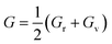
According to Density Functional Theory, a compound's behavior under various stress and other circumstances can be used to determine its mechanical properties.39 The mechanical properties of the GaBX3 compounds are shown in Table 6. The bulk modulus (B), shear modulus (G), Young's modulus (E), Poisson's ratio (v), and Pugh's ratio (B/G) of the compounds are all determined using the elastic stiffness constants Cij matrix.40 The following formulae were used to calculate the values, which are displayed in Table 6:41–43
| |
 | (9) |
| |
 | (10) |
| |
 | (11) |
Table 6 The mechanical characteristics of the compound GaBX3 (B = Cd, Zn and X = Cl, Br)
| Compounds |
Mechanical characteristics |
| Bulk modulus, B (GPa) |
Shear modulus, G (GPa) |
Young modulus, E (GPa) |
Poisson's ratio, ν |
Pugh's ratio B/G |
Machinability index, B/C44 |
Hardness Vickers, Hv |
| GaCdCl3 |
31.485 |
10.838 |
29.165 |
0.346 |
2.905 |
4.355 |
0.069 |
| GaCdBr3 |
25.883 |
9.133 |
24.515 |
0.342 |
2.834 |
4.259 |
0.071 |
| GaZnCl3 |
22.724 |
11.139 |
28.723 |
0.289 |
2.040 |
1.622 |
0.090 |
| GaZnBr3 |
29.623 |
13.581 |
35.343 |
0.301 |
2.181 |
2.233 |
0.086 |
The resistance in a material to compact when uniformly compressed is called bulk modulus (B). Larger B values imply more resistance to volumetric change with pressure. Shear modulus (G) indicates resistance to shear deformation and refers to material stiffness. The stiffness and elastic anisotropy are governed by Young's modulus (E) along the uniaxial stress. Higher E value means a higher stability of a material. ν is the Poisson ratio which describes how material deforms when it is stretched in one direction. The B/G ratio distinguishes between ductile and brittle materials. A higher ratio for a material indicates ductility, and a lower ratio indicates brittleness. The Vickers hardness (Hv) for the Ga-based halide perovskites studied was calculated from Poisson's ratio by means of a semi-empirical relationship,  44 which is used to correlate hardness and ductility.
GaCdCl3 has the largest bulk modulus of 31.485 GPa is also with greater resistance to volume compression. Volume compressibility is most sensitive in GaZnCl3 seems to be widely varied, which has lowest bulk modulus of 22.724 GPa (most wayward tendency). The bulk modulus of GaCdBr3 (25.883 GPa) and GaZnBr3 (29.623 GPa) are intermediate, suggesting relatively low compressibility. Shear modulus (G) for GaCdBr3 is the smallest of 9.133 GPa, making it the softest and highly elastic to shear deformation. On the other hand, GaZnBr3 has the largest G of 13.581 GPa representing the stiffest material among the investigated compounds. This trend is mirrored by the Young's modulus (E) values as well, where GaZnBr3 has the highest value of 35.343 GPa and GaCdBr3 has the lowest value of 24.515 GPa. It can be concluded that for GaCdX3 strength increases from Cl to Br but for GaZnX3 elasticity increases from Cl to Br. Fig. 6(a) represents a comparative study of the moduli for the GaBX3 compounds.
The Poisson's ratio (ν) shown in Fig. 5(b) ranges from 0.289 to 0.346 for the compounds GaBX3. It is noticeable that ν increased while changing X atom from Cl to Br for GaZnX3 but the effect is shown reverse in terms of GaCdX3. GaCdCl3 having the highest ν, indicates higher ductility and metal-like bonding,45 while GaZnCl3 with ν = 0.289 is relatively brittle and exhibits more covalent character. According to Pugh's ratio (B/G), all compounds have values greater than the ductile-to-brittle transition point of 1.75.46 This indicated that the compounds are ductile where GaCdCl3 with Pugh's ratio of 2.905 and GaCdBr3 of 2.834 are more ductile compared to GaZnCl3 of 2.040 and GaZnBr3 of 2.181.
 |
| | Fig. 5 (a) Comparative graphical representation of the elastic constants and (b) Poisson's ratio of the compounds GaBX3 (B = Cd, Zn and X = Cl, Br). | |
 |
| | Fig. 6 (a) Comparative graphical representation of the Pugh's ratio and (b) Kleinman parameter of the compounds GaBX3 (B = Cd, Zn and X = Cl, Br). | |
The machinability index (B/C44)44 reflects ease of mechanical processing. It is highest for GaCdCl3 that is 4.355, and lowest for GaZnCl3 which is 1.622. This implies that Cl-based compounds are more easily machinable than Br-based ones. The calculated Vickers hardness (HV) follows the inverse trend. Having the highest value of 0.090, GaZnCl3 confirms its maximum hardness and higher brittle nature. And GaCdCl3 has the lowest value of 0.069, indicating softness and high ductility.
3.4 Optical properties
3.4.1 Absorption. Absorption coefficient (α) is a measure of how strongly a material absorbs light per unit distance. It is a material property that defines how quickly the intensity of light decreases as it travels through the substance in a quantitative way.47 It is directly connected to the effectiveness of a material in terms of optoelectronics application.The photon energy (E) vs. absorption coefficient graph in Fig. 7 shows the absorption spectra of the materials GaBX3. It is seen that all the materials absorb photon energy in the mid UV to vacuum UV (4–124 eV) region.48 Two trends are noticeable here. Firstly, chloride compounds exhibit higher energy levels than the bromide ones and secondly, the bromide compounds show broader peaks than the chloride ones. All the compounds show lower absorption below 4 eV representing failure to overcome the energy required for forbidden transition of electrons. And the gradual decrease above 20 eV can be due to the overshooting of the electrons that can be explained by Fermi's Golden Rule. At higher photon energy the number of transition states and transition probability both decreases. Also, higher energy photons interact less efficiently with bound electrons.49 GaZnCl3 shows the highest peak at around 17 eV with an absorption coefficient of nearly 2.6 × 105 cm−1 that indicates strong transition of electrons from the halide 3p orbital to the metal (Zn) 4 s orbital. On the contrary, GaCdBr3 apparently shows the lowest peak in between 13–14 eV photon energy with an absorption coefficient close to 2.1 × 105 cm−1. This signifies weak transition of electrons from 4p (Br) to 4 s (Cd) orbital. However, the 4p orbital of Ga also has some contribution to the compounds electronic structure. The other two compounds GaCdCl3 and GaZnBr3 exhibit optical absorption profiles that fall within the spectral range limited by the two end-member compounds. Apparently the compound's application relies in the UV range where a high absorption power is required. The compounds can be useful in surgical tool disinfection, extreme ultraviolet (EUV) lithography, UV detectors and other optoelectronic devices.50–53
 |
| | Fig. 7 The calculated absorption coefficient of GaBX3 (B = Cd, Zn and X = Cl, Br). | |
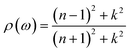
3.4.2 Reflectivity. Light returns to the medium from where it came when it strikes a material's surface. This phenomenon is known as reflectivity of a material, and it depends on how the material interacts with light and surface roughness.54 Fig. 8 shows the reflectivity spectrum ρ(ω)55 for GaBX3 which will help in understanding the reflective nature of the compounds.| |
 | (12) |
 |
| | Fig. 8 The reflectivity spectra of the compounds GaBX3. | |
The optical reflectivity (ρ) plotted as a function of photon energy (E) reveals distinct optical characteristics of the compounds.
Fig. 8 illustrates the reflectivity spectra of the distorted cubic halides GaBX3 over the photon energy range of 0–40 eV. The first strong peaks were found between 4–7 eV range gradually rising from the ground energy level. Strong dipole allowed the inter-band excitations, the halogen p to the metal s/p transition. The bromide compounds show slightly higher reflectivity than the chloride ones in this range because of the higher polarizability and diffusivity of the Br-4p orbital. In the mid-range, 8–17 eV, multiple oscillations have been observed where GaZnBr3 is the most pronounced among others. This could reflect the distorted structure of the compounds due to the crystal filed splitting and band folding, which lifts orbital degeneracy and allows several symmetry-permitted transitions from halogen p and metal d states to higher Ga-centered conduction states. Also, the hybridization of Cd-4d or Zn-3d orbitals are strong at this energy span. At high energy (18–22 eV) range chloride compounds show the highest and sharpest peaks compared to that of bromides because of the more localized orbitals of Cl. However, the maximum reflectivity is nearly 47% shown by GaZnCl3. The rapid decay of reflectivity beyond 22 eV indicates diminished inter-band transition density at higher energies. This refers to weak dielectric response, and the materials become increasingly transparent. Overall, diverse optical response of the compounds makes the bromide ones for UV and chloride ones for extreme-UV (EUV) potential for high-energy optoelectronic and photonic applications.56
3.4.3 Refractive index. The refraction is an important parameter to understand the bending of light inside a matter. Refractive index η(ω) is defined by the ratio of the velocity of light in a vacuum relative to the velocity of light passing through a material (the real part).57 Understanding these electronic and optical properties is critical for assessing how the compounds perform in diverse applications, ranging from photonic and optoelectronic devices to energy-related technologies.58| |
 | (13) |
Fig. 9 demonstrates the light-matter interaction quantified by the refractive index with two parts, real and imaginary. The real (η1) and imaginary (η2) parts of the refractive index of GaBX3 exhibit strong energy dependence that can be directly correlated with their electronic band structures and density of states. The negligible values of η2 for the compounds in the low-energy region (0–3 eV) indicate optical transparency below the fundamental band gap. A sharp increase in η2 between 3 to 5 eV refers to the inter-band transitions triggered from halogen p-derived valence states to Ga- and Zn/Cd-derived conduction bands. This maintains consistency with the calculated band gaps. However, because Br-4p orbital states have a larger energy and stronger delocalization than Cl-3p states, the bromide compounds have an earlier onset and higher absorption intensity. The transitions involving a high joint density of states, mainly from halogen p to metal s/p transitions, result in intense absorption peaks in the 5–12 eV region. Zn-based systems show enhanced η2 owing to stronger Zn-4s hybridization near the conduction band minimum. At higher energies (12–20 eV), broader features are associated with transitions from Ga-3d and Cd-4d semi-core states, as evidenced in the DOS.
 |
| | Fig. 9 The refractive index (a) real part (b) imaginary part of GaBX3 (B = Cd, Zn and X = Cl, Br). | |
The real part η1 represents the phase velocity reduction and dispersion of light due to electronic polarization. η1 exhibits anomalous dispersion near these absorption regions, showing sharp decreases at energies corresponding to η2 maxima, in agreement with Kramers Kronig relations.55 All the compounds show peak indices in the 2–6 eV region and afterwords scattering is observed. Highest static refractive index of GaZnBr3 compound, for both real and imaginary parts, reflects its increased electronic polarizability and faster electromagnetic propagation of wave. At photon energies above 25 eV, both η1 and η2 converge toward free-electron behavior due to diminished inter-band transition probability. In case of Cd, GaCdCl3 is dominant over GaCdBr3, and the scenario is opposite for GaZnX3. These results demonstrate that the optical response of these materials is governed by halogen-metal orbital hybridization and the distribution of electronic states across the valence and conduction bands.
3.4.4 Conductivity. The graphs in Fig. 10 represents σ1 and σ2 as the real and imaginary parts of conductivity on the vertical axis, measured in Siemens per meter (S m−1). Photon energy is captured on the horizontal axis, identified as ‘E' and measured in electron volts (eV). The property is calculated by using the following formula:59| |
 | (14) |
 |
| | Fig. 10 Conductivity (a) real part (b) imaginary part of GaBX3 (B = Cd, Zn and X = Cl, Br). | |
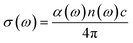
The experimental optical conductivity spectra, represented in Fig. 10(a), of the distorted cubic GaBX3 perovskites display a distinctly semiconducting character, with a very small σ1 at low photon energies, where the σ1 is drastically increasing after surpassing the optical band gap, at which point the inter-band electronic transitions begin to contribute to the σ1.60 Of the materials studied, GaZnCl3 shows the largest peak conductivity of nearly 6 S m−1, suggesting that it has a significant response to low-energy photons and would be a promising optoelectronic suitable to visible to near-UV devices. In GaZnBr3, a more distinct but also wider peak appears at 5.4 eV, which is attributed to better polarizability with the Br substitution. On the other hand, GaCdCl3 shows a strong peak of nearly 6 eV at a moderate intensity of 4.2 S m−1 and with higher energy secondary features, indicating multiple inter-band transitions associated with the Cd-d and Ga-s states. The peak at about 5–6 eV is larger and much wider which means the states are more delocalized and have lower transition probability for GaCdBr3. This results in the emergence of a number of peaks spanning across the spectrum, due in part to band splitting driven by distortion and strong metal-halide hybridization. However, differences in the energies of the transitions facilitate the effective absorption of photons and exciton generation. Based on these conductivity trends observed from an application point of view these materials are excellent potential candidate materials for applications such as UV photodetectors, light-harvesting devices, etc., as well as in optoelectronic functions for tunable absorption behavior.
Imaginary conductivity (σ2) shown in Fig. 10(b) contribute to the dispersive response of the carriers to an oscillating electromagnetic (EM) field and are important for polarization and energy storage. All compounds show simultaneously negative and positive broad features, which point to the transition between absorption-dominated and dispersion-dominated regimes.61 A strong negative minimum is found in the 4–7 eV range with values as small as −4.1 S m−1 (very high loss) for GaZnCl3 and GaZnBr3, elucidating the very strong phase retardation and intra-band polarization effects arising from lattice distortion. As the photon energy increases, σ2 crosses zero and attains positive maxima in the 15–22 eV region, with values approaching 2.5–3.0 S m−1, especially for the Zn-based systems, reflecting strong electronic polarization and coherent inter-band oscillations. These multiple dispersive features originate from complex electronic excitations and crystal-field effects induced by distorted cubic symmetry.
3.4.5 Dielectric function. The dielectric function ε(ω) describes how a material's optical and electrical activity is governed by an external, time-varying electric field. It connects the induced polarization to the applied electric field and defines important optical properties such as refractive index, absorption coefficient, reflectivity, and optical conductivity. In the frequency domain, the dielectric function is a complex quantity represented as| | |
ε(ω) = ε1(ω) + iε2(ω)
| (15) |
To determine the efficiency and performance levels, optoelectronic devices are highly dependent on the dielectric function.62
The real part of the dielectric function (ε1) describes the energy that can be stored in a material when an electric field is applied and thus yields vital information about its polarization behavior.55 For small photon energy ranging less than 5 eV, ε1 is close to zero, indicating that the polarization is not strong since incident light does not induce electrons across bandgap. A sudden jump of ε1 at 5–7 eV corresponds to the beginning of inter-band electronic transitions, that is, photons with an energy greater than band gap energy excite electron from valence band to conduction band leading to strong polarization as shown in Fig. 11(a). There are some notable differences between halide subclasses. The Cl-based perovskites have ε1 peaks at frequency nearly 6 eV while the Br counterparts (4–5 eV) occur at lower energies that are compatible with smaller band gaps. This indicates that Cl entails larger energy barrier for electron excitation. Between 10–15 eV, ε1 falls below zero, indicating the plasma edge, a characteristic trait of free carrier screening, where the material transitions from insulating to reflecting behavior. For higher energies greater than 15 eV, ε1 becomes of a small positive value, which means that the material is transparent as no further electronic transitions can occur. This feature makes cubic GaBX3 perovskites appealing for polarization-dependent optoelectronic devices, in which the ε1 can be tuned via halide substitution for flexible energy storage and field response.
 |
| | Fig. 11 The dielectric function (a) real part (b) imaginary part of GaBX3 (B = Cd, Zn and X = Cl, Br). | |
The imaginary part (ε2) directly measures the inter-band optical absorption, and its spectral characteristics are intimately connected to the electronic and vibrational dynamics.63 The sharp peaks of ε2 at 5–7 eV relate to the first onset of fundamental absorption edges and these are highly correlated with increasing ε1, in agreement with the Kramers–Kronig relation.64 The Br-based perovskites exhibit higher ε2 peak intensities with smaller absorption features compared to the Cl-containing systems, reflecting enhanced inter-band transition coherence and reduced electronic scattering associated with increased halide polarizability. A weak and broader feature above band edge (>7 eV), which can be attributed to the phonon scattering or defect states, hardly enhances the absorption. For photon energies above 10 eV, ε2 drops steeply to near zero since the excitation photons have not enough energy to induce band-to-band transitions. This behavior highlights the importance of halide composition on tuning absorption efficiency, rendering these perovskites interesting for light harvesting applications such as solar cells or LEDs.
3.4.6 Loss function. The loss function L(ω) describes the probability that a fast-moving charged particle such as an electron loses energy while traversing a material due to electronic excitations, particularly plasmon excitations. A plasmon is a collective oscillation of the free or valence electron density in a solid relative to the positively charged ion background. When an external electromagnetic field or a fast electron excites this collective motion at a characteristic frequency, the phenomenon is called plasmon resonance. Mathematically, plasmon resonance occurs at the energy ℏωp where the real part of the dielectric function vanishes:
| ε1(ωp) = 0 and ε2(ωp) ≪ 1 |
| |
 | (16) |
At this condition, electrons oscillate coherently, leading to strong energy absorption or loss.55,65 Understanding a material's optical and electronic characteristics is essential for high-energy and photonic applications.66 The following formula is used to determine the values.
Fig. 12 illustrates the photon energy on the x axis spanning 0 to 40 eV and loss function on the y axis. The prominent peaks observed around 18–21 eV originate from bulk plasmon resonances, which arise due to coherent oscillations of valence electrons. When the real part ε1(ω) of the dielectric function crosses zero the plasmon excitations are activated. This condition is intrinsically linked to the distribution of occupied and unoccupied electronic states across a wide energy window. At higher photon energies (15–25 eV), inter-band transitions from these deep-lying d and halogen p states to high-lying Ga-s/p conduction states accumulate, producing a large joint density of states (JDOS). This enhanced JDOS leads to strong polarization of the electron cloud, ultimately resulting in intense plasmon peaks in the loss spectra. From the plot it is seen that Zn-based compounds exhibit a higher plasmon strength. The highest strength for GaZnCl3 nearly 7.4 is due to the much more localized character of Zn-3d states relative to Cd-4d states. In contrast, bromide compounds show more widely ranging and less intense plasmon peaks from the combination of larger spatial extension and higher polarizability of Br-4p orbitals. This corresponds to the enhanced damping and energy broadening of the band. Thus, the differences in plasmon energy and intensity, and width of the plasmon peak for these compounds directly correspond to the various orbital hybridization, band dispersion as well as valence electron density obtained from DOS bandwidths and corresponding band structures.
 |
| | Fig. 12 The loss function of the compounds GaBX3 (B = Cd, Zn and X = Cl, Br). | |
3.5 Photocatalytic activity
The absolute positions of the CBM and VBM of GaBX3 (B = Cd, Zn; X = Cl, Br) were estimated using the Mulliken electronegativity approach in order to evaluate their redox capabilities, represented in Table 7.67
Table 7 The band edge energies EVB and ECB for photocatalytic activity
| Compounds |
χ (eV) |
Ee (eV) |
Eg (eV) |
EVB (eV) |
ECB (eV) |
| GaCdCl3 |
5.8 |
4.5 |
3.371 |
2.985 |
−0.386 |
| GaCdBr3 |
5.5 |
2.366 |
2.183 |
−0.183 |
| GaZnCl3 |
5.9 |
1.742 |
2.271 |
0.526 |
| GaZnBr3 |
5.6 |
0.648 |
1.424 |
0.776 |
The Mulliken electronegativity (χ) of each compound was calculated as the geometric mean of the electronegativities of its constituent elements, while the CBM and VBM positions were determined using the relations (17) and (18):4,68,69
| |
 | (17) |
where,
Ee = 4.5 eV represents the free-electron energy on the normal hydrogen electrode (NHE) scale. It is found that GaCdCl
3 has a bottom of valence band at 2.985 eV and top of conduction band at −0.386 eV, indicating strong oxidation strength but relatively good reduction potential. A similar feature is found for GaCdBr
3, which has the VBM and CBM of 2.183 eV and −0.183 eV, respectively. By contrast, GaZnCl
3 and GaZnBr
3 present positive CBM positions of 0.526 eV and 0.776 eV, respectively, reflecting a weaker reduction ability while they keep the VBM to be enough satisfied for oxidation reactions (2.271 eV for GaZnCl
3 and 1.424 eV for GaZnBr
3). The Cd-based GaBX
3 compounds, in brief, have more attractive redox character as compared with the Zn-based ones and a high suitableness for oxidation-reduction under photocatalysis process. Furthermore, the tunability of band gaps and proper band-edge positions as well as a stable perovskite structure imply that GaBX
3 materials are promising candidates for visible-light-driven photocatalyst or photodegradation, photoelectrochemical water splitting application, and optoelectronic equipment, such as photodetector.
70 These results show that B-site and X-site substitution can be used as an effective compositional strategy to selectively tune the redox chemistry in GaBX
3 based perovskite materials for further development of functional applied systems.
4
3.6 Thermal properties
A materials response to temperature fluctuations is demonstrated by the thermal characteristics calculated using the first-principle approached findings. Transverse velocity (Vt), longitudinal velocity (Vl), mean velocity (Vm), lattice thermal conductivity (Kph), minimum thermal conductivity (Kmin), Debye temperature (θD), and melting point (Tm) are some of these characteristics. The characteristics of the compound GaBX3 and its likely use in high-temperature conditions are discussed below.| |
 | (19) |
| |
 | (20) |
| |
 | (21) |
| |
 | (22) |
| |
 | (23) |
| |
 | (24) |
| | |
Tm = (554 + 5.911C11) ± 300 K
| (25) |
The speed at which transverse waves travel through a substance is known as the transverse sound velocity (Vt). Compressional or longitudinal waves propagate at a speed known as longitudinal sound velocity (Vl). The speed at which wave material may travel along fibers is known as longitudinal velocity, and the speed at which it can travel across fibers is known as transverse velocity.71 Therefore, the average of the two speeds is the mean velocity (Vm), which provides a useful indication of the wave's speed.72 Kph or lattice thermal conductivity is a measure of how easily a material transfers heat through lattice vibrations.73 Together, these parameters determine the lowest thermal conductivity, referred to as minimum thermal conductivity (Kmin), that can be achieved intrinsically by a material based on its atomic structure and density.74 The Debye temperature (θD) is a singular value for maximum vibrational density of a material. It is determined by the stiffness of a given material and the strength of bonding between lattices.75 Melting temperature (Tm) refers to the temperature at which solid transforms into liquid.76
The chloride-based compounds show better thermal and elastic properties than the bromide ones. Specifically, GaCdCl3 displays Vt and Vl of 1796.802 m s−1 and 3699.139 m s−1, respectively, which results in a mean sound velocity, Vm of 2018.975 m s−1 which suggests that the presence of relatively high acoustic velocities has correlated well with enhanced strong interatomic bonding as well as stiffness of elasticity. GaCdCl3 is consistently the utmost Debye temperature entry in this series with 240.595 K, more than likely due to a stiffer lattice and increased frequencies of vibration. In addition, GaCdCl3 also has a high lattice thermal conductivity of 9.228 W mK−1, meaning that the phonon-mediated heat transport is very efficient. With its melting point of 909.443 K, it has also proven to have excellent thermal stability, thus GaCdCl3 holds great promise as an efficient heat dissipation and thermal resistant material. Likewise, for GaZnCl3, significant thermal parameters were observed, with transverse, longitudinal, and average sound velocities of 1823.454 m s−1, 3349.091 m s−1, and 2034.028 m s−1, respectively. It is comparable to those of GaCdCl3 and indicative of rigid lattice, as given in Table 8. In agreement with the moderately strong bonding, the Debye temperature of GaZnCl3 is 173.097 K. Importantly GaZnCl3 has the largest lattice thermal conductivity of 9.914 W mK−1 among the four compounds studied. This implies that phonons are transported very efficiently in this material. With a melting temperature of 761.898 K, this makes it suitable for intermediate to high temperature thermal management applications, as well. On the other hand, for the Br-contained compounds, their thermal elastic properties decrease due to its bigger atomic mass and the promotion by this atom of phonon scatterings. GaZnBr3 has the sound velocities 1762.678 m s−1 (Vt) and 3304.512 m s−1 (Vl), resulting in an average speed of 1969.160 m s−1. The Debye temperature is about 228.969 K, representing a certain strong chemical bonding; nevertheless, its lattice thermal conductivities are as low as 7.774 W mK−1, implying that it has less phonon transference than the chloride analogs. The melting point of 852.347 K, shows that this compound possesses a quite satisfactory thermal stability but not so good as GaCdCl3. In this series, we find GaCdBr3 to possess the least thermal properties with Vt, Vl of 1476.594 m s−1, 3014.329 m s−1 respectively, and Vm of 1658.405 m s−1 suggesting a softer lattice as well as lowest overall thermal response among others. This is also manifested by its low Debye temperature of 173.444 K, which creates the relaxed lattice mode that enables more phonon scattering, leading to decrease in lattice thermal conductivity (6.559 W mK−1). Besides, GaCdBr3 exhibits the lowest melting temperature of 840.880 K and this makes it comparatively difficult to be used in high temperature techniques. These features imply that GaCdBr3 could be more applicable to devices with low thermal conductivities, for instance, a kind of thermal barrier or heat-insulation component.
Table 8 Calculated thermal properties of the compounds GaBX3 (B = Cd, Zn and X = Cl, Br)
| Compounds |
Vt (m s−1) |
Vl (m s−1) |
Vm (m s−1) |
θD (K) |
Kmin (W mK−1) |
Kpℎ (W mK−1) |
Tm (K) |
| GaCdCl3 |
1796.802 |
3699.139 |
2018.975 |
240.595 |
0.447 |
9.228 |
909.443 |
| GaCdBr3 |
1476.594 |
3014.329 |
1658.405 |
173.444 |
0.283 |
6.559 |
840.880 |
| GaZnCl3 |
1823.454 |
3349.091 |
2034.028 |
173.097 |
0.229 |
9.914 |
761.898 |
| GaZnBr3 |
1762.678 |
3304.512 |
1969.160 |
228.969 |
0.415 |
7.774 |
852.347 |
3.7 Thermodynamic stability
Decomposition energy (ΔEdec) represents the energy difference between a specific perovskite structure and its most stable competing phases.77,78 The thermodynamic stability of the halide compounds was assessed by calculating their decomposition energies with respect to their corresponding binary phases. Using the general decomposition pathway:
| GaBX3 → 0.43GaX3 + 0.57BX2, where B = Zn, Cd and X = Cl, Br. |
The corresponding energy of decomposition is defined by the total energy difference between the ternary compound and its binary constituents:
| ΔEdec = Ef(GaBX3) − [0.43Ef(GaX3) + 0.57Ef(BX2)] |
The calculated thermodynamic parameters for the materials are summarized in Table 9. All investigated ternary compounds exhibit negative decomposition energies, ranging from −0.166 eV per atom for GaCdBr3 to −0.189 eV per atom for GaCdCl3. Although the total energies indicate strong exothermicity reaching a minimum of −1.066 eV per atom for GaZnBr3 the sign of ΔEdec serves as the primary indicator of phase stability. Within this thermodynamic framework, a negative ΔEdec implies that the formation of the perovskite-like ternary phase is energetically favored over phase separation into its binary constituents (GaX3 and BX2). These results confirm that the GaBX3 halides are thermodynamically stable and exhibit strong resistance to spontaneous decomposition into their precursor binaries.2
Table 9 Decomposition energy of the compounds GaBX3
| Compounds |
Total energy (eV per atom) |
Decomposition energy (eV per atom) |
| CdCl2 |
−0.772 |
— |
| CdBr2 |
−0.799 |
— |
| ZnCl2 |
−0.878 |
— |
| ZnBr2 |
−0.905 |
— |
| GaCl3 |
−0.855 |
— |
| GaBr3 |
−0.885 |
— |
| GaCdCl3 |
−0.997 |
−0.189 |
| GaCdBr3 |
−1.002 |
−0.166 |
| GaZnCl3 |
−1.041 |
−0.173 |
| GaZnBr3 |
−1.066 |
−0.170 |
3.8 Phonon dispersion
Phonon dispersion is the physical phenomenon that describes the relationship between energy and quadratic components of momentum for phonons within a crystal lattice, whereby these quasiparticles serve as one of the crucial measurements to understand material dynamic and vibrational properties.79 Subsequent to phonon spectra evaluation, full structural optimization of the lattice parameters and atomic coordinates were performed for computational accuracy. This work focuses on the dynamical properties of GaBX3 materials, offering elastic dispersion relations which enable a robust description of their lattice dynamics. As shown in Fig. 13, the dispersion curves are plotted over the high-symmetry directions Γ-X-M-Γ-X in first Brillouin zone. The horizontal axis identifies these symmetry-specific k-point trajectories, while the vertical axis quantifies the phonon energy levels, representing the lattice's response to external perturbations, such as the oscillating electric fields associated with incident electromagnetic radiation.
 |
| | Fig. 13 Phonon dispersion curves of the compounds GaBX3 (B = Cd, Zn and X = Cl, Br). | |
In the GaCdX3 these imaginary frequencies reach values near −5 THz, whereas the Zn-based counterparts, particularly GaZnBr3, show even more drastic instabilities with modes dropping to approximately −11 THz. These negative frequencies at 0 K indicate that the high-symmetry cubic Pmm phase does not represent a local energy minimum but rather a saddle point on the potential energy surface. While thermodynamic and mechanical stability criteria are satisfied, the phonon results unambiguously reveal that the cubic structures alone correspond to metastable states that can stabilize only under finite temperature effects, anharmonic lattice vibrations or external conditions like pressure. These results demonstrate that lattice dynamics can influence the actual structural stability of GaBX3 perovskites significantly. However, a similar work NaWO3 and CsSnI3 were physically synthesized, theoretical studies revealed negative phonon frequencies.80,81 Also, negative phonon frequencies were observed at 0 K but at higher temperature the stabilized paraelectric phase was found for BaTiO3 and SrTiO3 when physically synthesized.82,83
3.9 Magnetic properties
In the corresponding calculated band structures, α and β channels are for spin-up and spin-down electronic states, respectively as shown in Fig. 14. We see a full overlap of the α and β bands in the entire Brillouin Zone, pointing at no spin-splitting at all high-symmetry points. This degeneracy in the spin channel indicates that these compounds are non-magnetic or diamagnetic. Meaning, all electrons are paired and the net magnetic moment is zero. A well-defined band gap exists around the Fermi level, with the occupied valence bands lying below it and higher unoccupied conduction bands above it. The absence of a crossing between any bands and the Fermi level indicates that these materials are semiconductors or insulators, but not metals.
 |
| | Fig. 14 Magnetic band structure of the compounds GaBX3 (B = Cd, Zn and X = Cl, Br). | |
The magnetic density of states in Fig. 15 provides further evidence of this phenomenon. The α (positive DOS) and β (negative DOS) components are perfectly mirror symmetric with respect to the zero–energy axis that supports the disappearing net spin polarization and confirm that it is a diamagnetic ground state. It is worth pointing out that the total DOS cancels at the Fermi energy for both spin polarizations, confirming also the existence of a finite band gap and clarifying the semiconducting character of these systems.84 Strong DOS peaks can be found in the deep valence region at around −12 to −14 eV, which are contributed mainly from halogen p states, and two other dominant features near −7 to −5 eV and −2 to 0 eV due to Cd or Zn d orbitals hybridizing with Ga p states. The observation of the closure in α and β spin channels can also confirm their diamagnetic behavior and hence, their electronic properties are not influenced by either spin polarization or exchange. This is important as for DFT an erroneously applied magnetic configuration can cause spurious band splitting and erroneous band gap predictions. Their non-magnetic nature enables spin-independent transport in optoelectronic and dielectric devices while providing a robust background for studying dopant, defect or strain-induced magnetism.60,85
 |
| | Fig. 15 Magnetic density of states of the compounds GaBX3 (B = Cd, Zn and X = Cl, Br). | |
3.10 Population analysis
Table 10 provides a complete overview of the charge distribution and bonding properties of GaBX3 (B = Cd, Zn; X = Cl, Br) compounds, based on Mulliken atomic populations, Mulliken charges, Hirshfeld charges, and charge spilling percentages. The population analysis shows a predominant mixed ionic–covalent bonding nature dictated by halogen electronegativity and B-site chemistry. The only very small charge spilling (0.11–0.16%) also ensure the reliability of the orbital projection and validate the Mulliken populations.86 In all complexes, the halogen atoms show prevalent p-orbital occupancy and negative Mulliken and Hirshfeld charges, indicating their behavior as electron acceptors; such anionic character is stronger for Cl in comparison to Br due to the higher electronegativity of chlorine. Gallium, however, maintains a positive charge across all compositions, with its filled d states playing the role of chemically inert cores and a mixed population s–p contributing to Ga–X bonding; this provides strong evidence for considerable orbital hybridization in the cubic phase. The B-site cations' behavior in relation to composition is found to be composition dependent: whereas Cd shows a moderate positive charge and suggests more ionic nature of the Cd–X interaction, with decreasing effective charge and molecular participation for Zn, it implies stronger covalent bonding. The replacement of Cl by Br successively decreases the charge transfer and ionicity and increases covalent nature without disturbing cubic symmetry. In summary, the Mulliken and Hirshfeld analyses together show that the electronic structure stabilization of cubic GaBX3 perovskites arises from an ionic backbone modulated by sizable covalent contributions, which is important to understand their electronic dispersion. This population analysis rationalizes the charge transfer and bonding characters in the cubic perovskites, revealing ionic and covalent contributions. By varying the B-site cation, and halogen substitution, we show how ionicity and hybridization can be systematically adjusted. They are crucial for composition dependence on electronic structure and optoelectronic properties.26
Table 10 Population analysis for the compounds GaBX3 (B = Cd, Zn; X = Cl, Br)
| Compound |
Charge spilling (%) |
Species |
Mulliken atomic populations |
Mulliken charge |
Hirshfeld charge |
| s |
p |
d |
f |
Total |
| GaCdCl3 |
0.14 |
Cl |
1.94 |
5.54 |
0.00 |
0.00 |
7.49 |
−0.49 |
−0.26 |
| Ga |
1.76 |
0.35 |
10.00 |
0.00 |
12.11 |
0.89 |
0.40 |
| Cd |
0.68 |
0.77 |
9.99 |
0.00 |
11.44 |
0.56 |
0.38 |
| GaCdBr3 |
0.11 |
Br |
1.73 |
5.46 |
0.00 |
0.00 |
7.20 |
−0.20 |
−0.24 |
| Ga |
2.02 |
0.42 |
10.00 |
0.00 |
12.43 |
0.57 |
0.39 |
| Cd |
0.97 |
1.02 |
9.99 |
0.00 |
11.98 |
0.02 |
0.34 |
| GaZnCl3 |
0.16 |
Cl |
1.93 |
5.48 |
0.00 |
0.00 |
7.42 |
−0.42 |
−0.22 |
| Ga |
1.83 |
0.41 |
10.00 |
0.00 |
12.23 |
0.77 |
0.32 |
| Zn |
0.66 |
0.86 |
9.99 |
0.00 |
11.51 |
0.49 |
0.33 |
| GaZnBr3 |
0.13 |
Br |
1.71 |
5.40 |
0.00 |
0.00 |
7.11 |
−0.11 |
−0.20 |
| Ga |
2.03 |
0.50 |
10.00 |
0.00 |
12.53 |
0.47 |
0.32 |
| Zn |
1.04 |
1.11 |
9.99 |
0.00 |
12.14 |
−0.14 |
0.29 |
4. Conclusion
This study investigated the suitability of lead-free Ga-based halide perovskites GaBX3 (B = Cd, Zn; X = Cl, Br) as multifunctional materials for optoelectronic and photocatalytic applications. Using first-principles Density Functional Theory calculations, including GGA-PBE structural optimization and HSE06 electronic corrections, structural stability, electronic band structure, optical response, mechanical robustness, thermal behavior, magnetic nature, and photocatalytic redox capability were examined. The results confirm that all compounds are thermodynamically and mechanically stable cubic perovskites with negative formation enthalpy and ductile characteristics. The band gaps were found to be widely tunable from 0.65 up to 3.37 eV, enabling application-specific selection. Bromide substitution narrows the band gap while chloride enhances rigidity and thermal stability. Optical analysis revealed strong UV-visible absorption and favorable dielectric response, whereas band-edge alignment demonstrated promising visible-light water-splitting potential, especially for Cd-based systems. The original goal of this research was to identify environmentally benign alternatives to toxic lead perovskites that simultaneously maintain high optoelectronic performance and structural reliability. The phonon dispersion analysis indicates that the high-symmetry cubic phase represents a metastable state at 0 K, evidence from analogous systems suggests stability under finite temperature or external pressure. This work demonstrates that our investigated GaBX3 compounds are stable and tunable. These multifunctional materials are expected for photodetector, light-harvesting device and photocatalytic hydrogen generation. From a social perspective, the non-toxic perovskites reduce environmental pollution due to lead-based materials for safe applications of renewable energy facilities and green electronics. This research can be further developed by the investigation on defect engineering, strain modulation, heterostructure design and experimental synthesis verification for other researchers. Moreover, doped magnetism and device simulations may promote the development of high-performance devices for practical clean energy applications.
Authors contribution
S. M. Shamsuddoha performed the primary investigation, developed the methodology, managed data curation and wrote the original draft. Tashikur Rahman contributed to conceptualization, formal analysis, and draft preparation. Istiak Ahmed Ovi was responsible for formal analysis, validation, and reviewing. Shapnarup Bandhya assisted with data curation, reviewing, and editing.
Conflicts of interest
The authors declare that they have no known competing financial interests or personal relationships that could have appeared to influence the work reported in this paper.
Data availability
The data that support the findings of this study are available from the corresponding author upon reasonable request.
Supplementary information (SI) is available. See DOI: https://doi.org/10.1039/d6ra01845a.
Acknowledgements
This work was performed at the Computational Materials Science Laboratory, Department of Materials Science and Engineering, Khulna University of Engineering and Technology (KUET), Khulna 9203, Bangladesh.
References
- C. Zhang, D. Kuang and W. Wu, A Review of Diverse Halide Perovskite Morphologies for Efficient Optoelectronic Applications, Small Methods, 2020, 4(2), 1900662, DOI:10.1002/smtd.201900662.
- M. Faghihnasiri, M. Izadifard and M. E. Ghazi, DFT Study of Mechanical Properties and Stability of Cubic Methylammonium Lead Halide Perovskites (CH3 NH3 PbX3 , X = I, Br, Cl), J. Phys. Chem. C, 2017, 121(48), 27059–27070, DOI:10.1021/acs.jpcc.7b07129.
- M. V. Kovalenko, L. Protesescu and M. I. Bodnarchuk, Properties and potential optoelectronic applications of lead halide perovskite nanocrystals, Science, 2017, 358(6364), 745–750, DOI:10.1126/science.aam7093.
- M. Aktary, M. Kamruzzaman and R. Afrose, A comparative study of the mechanical stability, electronic, optical and photocatalytic properties of CsPbX3 (X = Cl, Br, I) by DFT calculations for optoelectronic applications, RSC Adv., 2022, 12(36), 23704–23717, 10.1039/D2RA04591E.
- M. Riaz, S. M. Ali, N. Bano, S. D. Ali and M. A. Shakoori, DFT insights into multifaceted properties of GaCaX3 (X = Cl, Br, I) inorganic cubic halide perovskites for advanced optoelectronic applications, Comput. Theor. Chem., 2025, 1243, 114993, DOI:10.1016/j.comptc.2024.114993.
- M. Radjai, et al., Computational investigation of the structural, elastic, electronic, and thermodynamic properties of chloroperovskites GaXCl3 (X = Be, Ca, or Sr) using DFT framework, Phys. Scr., 2024, 99(6), 065917, DOI:10.1088/1402-4896/ad418b.
- Z. Khan, Insight into the Physical Properties of Lead-free Chloroperovskites GaXCl3 (X = Be, Ca) Compounds: Probed by DFT, Opt. Quantum Electron., 2024, 836 CrossRef CAS.
- I. A. Apon, R. Hasan, Md and M. Islam, First-principles investigation of structural, mechanical, and electronic properties of AMgX3 (A=Ga, In, Tl, and X=Cl, Br, I) perovskites for optoelectronic applications, Phys. Scr., 2025, 100(1), 015931, DOI:10.1088/1402-4896/ad966f.
- S. H. Shah, et al., Investigation of structure, optoelectronic, and thermodynamic properties of gallium-based perovskites GaMF3 (M= Ca, and Cd) for solar cell applications, Opt. Quantum Electron., 2024, 56(9), 1461 CrossRef CAS.
- A. Habib, et al., Insight into the exemplary physical properties of Zn-based fluoroperovskite compounds XZnF3 (X= Al, Cs, Ga, In) employing accurate GGA approach: a first-principles study, Materials, 2022, 15(7), 2669 CrossRef CAS PubMed.
- S. J. Clark, et al., First principles methods using CASTEP, Z. fur Krist.-Cryst. Mater., 2005, 220(5–6), 567–570, DOI:10.1524/zkri.220.5.567.65075.
- J. P. Perdew, K. Burke and M. Ernzerhof, Generalized Gradient Approximation Made Simple, Phys. Rev. Lett., 1996, 77(18), 3865–3868, DOI:10.1103/PhysRevLett.77.3865.
- D. Vanderbilt, Soft self-consistent pseudopotentials in a generalized eigenvalue formalism, Phys. Rev. B Condens. Matter, 1990, 41(11), 7892–7895, DOI:10.1103/PhysRevB.41.7892.
- P. E. Van Camp and V. E. Van Doren, Total energy calculations in the DFT on binary compounds, Int. J. Quantum Chem., 1995, 55(4), 339–345, DOI:10.1002/qua.560550405.
- H. J. Monkhorst and J. D. Pack, Special points for Brillouin-zone integrations, Phys. Rev. B Condens. Matter, 1976, 13(12), 5188–5192, DOI:10.1103/PhysRevB.13.5188.
- T. H. Fiscber and J. Almlof, General methods for geometry and wave function optimization, J. Phys. Chem., 1992, 96, 7 Search PubMed.
- G. Lippert, J. Hutter, P. Ballone and M. Parrinello, Response Function Basis Sets: Application to Density Functional Calculations, J. Phys. Chem., 1996, 100(15), 6231–6235, DOI:10.1021/jp9527766.
- K. Momma and F. Izumi, VESTA 3 for three-dimensional visualization of crystal, volumetric and morphology data, J. Appl. Crystallogr., 2011, 44(6), 1272–1276 CrossRef CAS.
- I. Khan, A. Ullah, N. Rahman, M. Husain, V. Tirth and M. Sohail, First principle study of structural and optoelectronic properties of ZnLiX3 (X = Cl or F) perovskites, Results Phys., 2024, 66, 108019, DOI:10.1016/j.rinp.2024.108019.
- Md. H. Miah, M. U. Khandaker, Md. B. Rahman, M. Nur-E-Alam and M. A. Islam, Band gap tuning of perovskite solar cells for enhancing the efficiency and stability: issues and prospects, RSC Adv., 2024, 14(23), 15876–15906, 10.1039/D4RA01640H.
- Andselisk, Answer to “How to get ionic radii for coordination number 12?”, Chemistry Stack Exchange, accessed: Apr. 06, 2026. https://chemistry.stackexchange.com/a/107813.
- R. D. Shannon, Revised effective ionic radii and systematic studies of interatomic distances in halides and chalcogenides, Acta Crystallogr., Sect. A, 1976, 32(5), 751–767 CrossRef.
- G. Moschou, A. Koliogiorgos and I. Galanakis, Electronic Properties of Cs-Based Halide Perovskites: An Ab Initio Study, Phys. Status Solidi A, 2018, 215(17), 1700941, DOI:10.1002/pssa.201700941.
- Z. Khan, et al., Insight into the physical properties of lead-free Chloroperovskites GaXCl3 (X = Be, Ca) compounds: probed by DFT, Opt. Quantum Electron., 2024, 56(5), 836, DOI:10.1007/s11082-024-06345-3.
- B. M. Ilyas and B. H. Elias, A theoretical study of perovskite CsXCl3 (X=Pb, Cd) within first principles calculations, Phys. B, 2017, 510(Apr), 60–73, DOI:10.1016/j.physb.2016.12.019.
- S. M. Shamsuddoha, S. Bandhya, I. A. Ovi and T. Rahman, First-principles investigation of next-generation lead-free InXCl3 halide perovskites, AIP Adv., 2025, 15(12), 125319, DOI:10.1063/5.0304552.
- L. K. Lamontagne, Band Structures and the Meaning of the Wave Vector K, 2018 Search PubMed.
- Md. B. H. Parosh, et al., DFT Investigations of Non-Toxic Perovskites RbZnX3 (X = F, Cl, and Br): Analyzing the Structural, Electrical, Optical, Mechanical, and Thermodynamic Properties for Suitable Optoelectronic Applications, Int. J. Quantum Chem., 2025, 125(4), e70014, DOI:10.1002/qua.70014.
- Md. S. Sorker, Md. R. Islam, A. Chakraborty and Md. A. Razzak Sarker, First-principles and experimental study to investigate structural, elastic, electronic, thermal, and optical properties of KCdCl3 metal halide perovskite crystals, AIP Adv., 2024, 14(4), 045038, DOI:10.1063/5.0206191.
- S. Idrissi, S. Ziti, H. Labrim and L. Bahmad, Band gaps of the solar perovskites photovoltaic CsXCl3 (X=Sn, Pb or Ge), Mater. Sci. Semicond. Process., 2021, 122, 105484, DOI:10.1016/j.mssp.2020.105484.
- G. Hodes, Perovskite-Based Solar Cells, Science, 2013, 342(6156), 317–318, DOI:10.1126/science.1245473.
- X. Liu, J. Fu, M. M. Han, K. X. Sun and S. L. Wei, First-Principles Study on Electronic Structure, Elasticity, Debye Temperature and Anisotropy of Cubic KCaF3, MSF, 2020, 999, 109–116, DOI:10.4028/www.scientific.net/MSF.999.109.
- C. T. Walker, Solid State Physics over 13 Years: Introduction to Solid State Physics. Charles Kittel. Wiley, New York, edn 3, 1966, 662 pp., illus. $12.50., Science, 155, 3765, 991–991, 1967 Search PubMed.
- F. Mouhat and F.-X. Coudert, Necessary and sufficient elastic stability conditions in various crystal systems, Phys. Rev. B Condens. Matter, 2014, 90(22), 224104, DOI:10.1103/PhysRevB.90.224104.
- F. D. Murnaghan, Finite Deformations of an Elastic Solid, Am. J. Math., 1937, 59(2), 235–260, DOI:10.2307/2371405.
- N. Coburn, Review of Finite Deformations of an Elastic Solid, Math. Mag., 1953, 27(2), 109–111, DOI:10.2307/3029772.
- T. E. Jones, T. C. R. Rocha, A. Knop-Gericke, C. Stampfl, R. Schlögl and S. Piccinin, Adsorbate induced vacancy formation on silver surfaces, Phys. Chem. Chem. Phys., 2014, 16(19), 9002–9014, 10.1039/C4CP00778F.
- M. A. Islam, J. Islam, M. N. Islam, S. K. Sen and A. K. M. A. Hossain, Enhanced ductility and optoelectronic properties of environment-friendly CsGeCl3 under pressure, AIP Adv., 2021, 11(4), 045014, DOI:10.1063/5.0048849.
- Z. B. Wang, B. S. Luk’yanchuk, M. H. Hong, Y. Lin and T. C. Chong, Energy flow around a small particle investigated by classical Mie theory, Phys. Rev. B Condens. Matter, 2004, 70(3), 035418, DOI:10.1103/PhysRevB.70.035418.
- A. Bouhemadou, Calculated structural, electronic and elastic properties of M2GeC (M=Ti, V, Cr, Zr, Nb, Mo, Hf, Ta and W), Appl. Phys. A, 2009, 96(4), 959–967, DOI:10.1007/s00339-009-5106-5.
- R. Hill, The elastic behaviour of a crystalline aggregate, Proc. Phys. Soc., London, Sect. A, 1952, 65(5), 349 CrossRef.
- M. Al-Fahdi, A. Rodriguez, T. Ouyang and M. Hu, High-throughput computation of new carbon allotropes with diverse hybridization and ultrahigh hardness, Crystals, 2021, 11(7), 783 CrossRef CAS.
- T. Rahman, I. A. Ovi, S. M. Shamsuddoha and S. Bandhya, First-principles investigation of the structural, electronic, thermal, and mechanical properties of radium-based halide perovskites: A DFT study, AIP Adv., 2026, 16(2), 025339 CrossRef CAS , accessed: Apr. 06, 2026. https://pubs.aip.org/aip/adv/article/16/2/025339/3380866.
- I. A. Apon, et al., Unveiling the Electronic, Optical, and Mechanical Properties of Lithium-Based Perovskites for Next-Generation Solar Cells, J. Inorg. Organomet. Polym., 2025 DOI:10.1007/s10904-025-03957-4.
- X. Diao, et al., High-throughput screening of stable and efficient double inorganic halide perovskite materials by DFT, Sci. Rep., 2022, 12(1), 12633, DOI:10.1038/s41598-022-16221-3.
- A. V. Shatov, S. S. Ponomarev, and S. A. Firstov, Hardness and deformation of hardmetals at room temperature, in Comprehensive Hard Materials, 2014, pp. 267–299, accessed: Jan. 31, 2026. https://elibrary.ru/item.asp?id=24480635 Search PubMed.
- J. I. Pankove, Optical Processes in Semiconductors, Courier Corporation, 2012, accessed: Dec. 24, 2025. https://books.google.com/books?hl=en%26lr=%26id=Tg3DAgAAQBAJ%26oi=fnd%26pg=PA1%26dq=J.+I.+Pankove,+Optical+Processes+in+Semiconductors.+New+York:+Dover,+1971.%26ots=_FFS6VPM_H%26sig=KEtOLJWUDCD_3_8BIDTsz23mOKE Search PubMed.
- W. Tobiska and A. Nusinov, ISO 21348 - Process for determining solar irradiances, Presented at the 36th COSPAR Scientific Assembly, 2006, 2621, accessed: Dec. 23, 2025. https://ui.adsabs.harvard.edu/abs/2006cosp...36.2621T Search PubMed.
- J.-M. Zhang and Y. Liu, Fermi's golden rule: its derivation and breakdown by an ideal model, Eur. J. Phys., 2016, 37(6), 065406 CrossRef.
- M. D. Hasan, I. A. Apon, I. A. Ovi and M. S. Haque, Calculations of the mechanical, optoelectronic, and magnetic properties of FrGeX3 (X= Cl, Br, I) under hydrostatic pressures based on first-principles theories, AIP Adv., 2024, 14(3), 035341 CrossRef CAS , accessed: Dec. 24, 2025. https://pubs.aip.org/aip/adv/article/14/3/035341/3277997.
- N. Fu, Y. Liu, X. Ma and Z. Chen, EUV lithography: State-of-the-art review, J. Microelectron. Manuf., 2019, 2(2), 1–6 Search PubMed.
- A. P. Robinson and R. A. Lawson, Alternative resist approaches, in Frontiers of Nanoscience, Elsevier, 2016, 11, pp. 447–478, accessed: Dec. 24, 2025. https://www.sciencedirect.com/science/article/pii/B9780081003541000132 Search PubMed.
- A. Shehzad, et al., Photoresist absorption measurement at extreme ultraviolet (EUV) wavelength by thin film transmission method, J. Photopolym. Sci. Technol., 2019, 32(1), 57–66 CrossRef CAS.
- C. Hu, et al., Optical coatings of durability based on transition metal nitrides, Thin Solid Films, 2019, 688, 137339 CrossRef CAS.
- M. Fox, Optical Properties of Solids, Oxford university press, 2010, 3, accessed: Dec. 29, 2025. https://books.google.com/books?hl=en%26lr=%26id=5WkVDAAAQBAJ%26oi=fnd%26pg=PP1%26dq=M.+Fox,+Optical+Properties+of+Solids,+2nd+ed.,+Oxford+University+Press+(2010),+Chapter+2.%26ots=v56Llf6zNF%26sig=AKkzQzJoMiiHdVNTpU0SHTIs2Ug Search PubMed.
- M. Roknuzzaman, K. (Ken) Ostrikov, H. Wang, A. Du and T. Tesfamichael, Towards lead-free perovskite photovoltaics and optoelectronics by ab initio simulations, Sci. Rep., 2017, 7(1), 14025, DOI:10.1038/s41598-017-13172-y.
- C. Raymond and S. Ronca, Relation of structure to electrical and optical properties, in Brydson's Plastics Materials, Elsevier, 2017, pp. 103–125, accessed: Dec. 29, 2025. https://www.sciencedirect.com/science/article/pii/B9780323358248000062 Search PubMed.
- Md. M. Rahaman, et al., Mechanical, electronic, optical, and thermodynamic properties of orthorhonmbic LiCuBiO4 crystal: a first–priciples study, J. Mater. Res. Technol., 2019, 8(5), 3783–3794, DOI:10.1016/j.jmrt.2019.06.039.
- M. Dressel and G. Grüner, Electrodynamics of Solids: Optical Properties of Electrons in Matter. Cambridge university press, 2002, accessed: Jan. 24, 2026. https://books.google.com/books?hl=en%26lr=%26id=Wv-wrtRdWT0C%26oi=fnd%26pg=PR9%26dq=Electrodynamics+of+Solids:+Optical+Properties+of+Electrons+in+Matter,+Cambridge,+U.K%26ots=7NcQPVhMiP%26sig=ATypI5rtkGoxB5Z3odaugT-XRs8 Search PubMed.
- R. M. Martin, Electronic Structure: Basic Theory and Practical Methods. Cambridge university press, 2020 Search PubMed.
- Y. U. Peter and M. Cardona, Fundamentals of Semiconductors: Physics and Materials Properties. Springer Science & Business Media, 2010, accessed: Jan. 24, 2026. https://books.google.com/books?hl=en%26lr=%26id=5aBuKYBT_hsC%26oi=fnd%26pg=PR6%26dq=P.+Y.+Yu+and+M.+Cardona,+Fundamentals+of+Semiconductors:+Physics+and+Materials+Properties,+4th+ed.,+Berlin,+Germany:+Springer,+2010.%26ots=KgDsusXmBU%26sig=4uTNRfjQZseLUjCNcJurSd0dJ8g Search PubMed.
- S. Saha, T. P. Sinha and A. Mookerjee, Structure, structural phase transitions, mechanical properties, defects, etc.-Electronic structure, chemical bonding, and optical properties of paraelectric BaTiO3, Phys. Rev. B Condens. Matter, 2000, 62(13), 8828–8834 CrossRef CAS.
- S. L. Adler, Quantum Theory of the Dielectric Constant in Real Solids, Phys. Rev., 1962, 126(2), 413–420, DOI:10.1103/PhysRev.126.413.
- M. Gajdoš, K. Hummer, G. Kresse, J. Furthmüller and F. Bechstedt, Linear optical properties in the projector-augmented wave methodology, Phys. Rev. B Condens. Matter, 2006, 73(4), 045112, DOI:10.1103/PhysRevB.73.045112.
- R. H. Ritchie, Plasma Losses by Fast Electrons in Thin Films, Phys. Rev., 1957, 106(5), 874–881, DOI:10.1103/PhysRev.106.874.
- S. Boucetta, Theoretical study of elastic, mechanical and thermodynamic properties of MgRh intermetallic compound, J. Magnesium Alloys, 2014, 2(1), 59–63, DOI:10.1016/j.jma.2014.04.001.
- Y. Gong, H. Yu and X. Quan, Origin of Visible Light Photocatalytic Activity of Ag 3 AsO 4 from First-Principles Calculation, Int. J. Photoenergy, 2014, 2014, 1–5, DOI:10.1155/2014/639509.
- J. Liu, S. Chen, Q. Liu, Y. Zhu and J. Zhang, Correlation of crystal structures and electronic structures with visible light photocatalytic properties of NaBiO3, Chem. Phys. Lett., 2013, 572, 101–105, DOI:10.1016/j.cplett.2013.04.040.
- W. Zulfiqar, S. M. Alay-e-Abbas, G. Abbas, A. Laref, J. A. Larsson and A. Shaukat, Revisiting the structural, electronic and photocatalytic properties of Ti and Zr based perovskites with meta-GGA functionals of DFT, J. Mater. Chem. C, 2021, 9(14), 4862–4876, 10.1039/D0TC05964A.
- X. Chen, S. Shen, L. Guo and S. S. Mao, Semiconductor-based Photocatalytic Hydrogen Generation, Chem. Rev., 2010, 110(11), 6503–6570, DOI:10.1021/cr1001645.
- APPROXIMATIONS TO THE REFLECTION AND TRANSMISSION COEFFICIENTS OF PLANE LONGITUDINAL AND TRANSVERSE WAVES* | Earthdoc. accessed: Dec. 04, 2024. https://www.earthdoc.org/content/journals/10.1111/j.1365-2478.1961.tb01670.x.
- S. J. Schön, Chapter 9 - Thermal Properties, in Handbook of Petroleum Exploration and Production, ed.J. H. Schön, in Physical Properties of Rocks, Elsevier, 2011, 8, pp. 337–372. DOI:10.1016/S1567-8032(11)08009-8.
- G. A. Slack, The Thermal Conductivity of Nonmetallic Crystals, in Solid State Physics, ed. H. Ehrenreich, F. Seitz, and D. Turnbull, Academic Press, 1979, 34, pp. 1–71. DOI:10.1016/S0081-1947(08)60359-8.
- Phys. Rev. B Condens. Matter46, 6131 ( 1992) - Lower limit to the thermal conductivity of disordered crystals, accessed: Dec. 04, 2024. https://journals.aps.org/prb/abstract/10.1103/PhysRevB.46.6131 Search PubMed.
- The law of Dulong and Petit | J. Chem. Educ., accessed: Oct. 13, 2024. https://pubs.acs.org/doi/abs/10.1021/ed037p545 Search PubMed.
- Melting temperature prediction via first principles and deep learning - ScienceDirect, accessed: Dec. 04, 2024, https://www.sciencedirect.com/science/article/abs/pii/S0927025622004128.
- W. Sun, et al., The thermodynamic scale of inorganic crystalline metastability, Sci. Adv., 2016, 2(11), e1600225, DOI:10.1126/sciadv.1600225.
- C.-J. Yu, Advances in modelling and simulation of halide perovskites for solar cell applications, J. Phys.: Energy, 2019, 1(2), 022001 CAS.
- S. M. Shamsuddoha, S. Bandhya, I. A. Ovi and T. Rahman, First-principles investigation of next-generation lead-free InXCl3 halide perovskites, AIP Adv., 2025, 15(12), 125319 CrossRef CAS , accessed Apr. 06, 2026. https://pubs.aip.org/aip/adv/article/15/12/125319/3374701.
- C. Çoban, First-Principles Study on Structural, Electronic, Elastic, Phonon, and Thermodynamic Properties of Tungsten Oxide-Based Perovskite NaWO3, J. Electron. Mater., 2021, 50(9), 5402–5411, DOI:10.1007/s11664-021-09068-3.
- L. Monacelli and N. Marzari, First-Principles Thermodynamics of CsSnI3, Chem. Mater., 2023, 35(4), 1702–1709, DOI:10.1021/acs.chemmater.2c03475.
- S. Ehsan, M. Arrigoni, G. K. H. Madsen, P. Blaha and A. Tröster, First-principles self-consistent phonon approach to the study of the vibrational properties and structural phase transition of BaTiO 3, Phys. Rev. B Condens. Matter, 2021, 103(9), 094108, DOI:10.1103/PhysRevB.103.094108.
- C. Verdi, L. Ranalli, C. Franchini and G. Kresse, Quantum paraelectricity and structural phase transitions in strontium titanate beyond density functional theory, Phys. Rev. Mater., 2023, 7(3), L030801, DOI:10.1103/PhysRevMaterials.7.L030801.
- Md. B. H. Parosh, et al., DFT Investigations of Non-Toxic Perovskites RbZnX3 (X = F, Cl, and Br): Analyzing the Structural, Electrical, Optical, Mechanical, and Thermodynamic Properties for Suitable Optoelectronic Applications, Int. J. Quantum Chem., 2025, 125(4), e70014, DOI:10.1002/qua.70014.
- J. Kübler, Theory of Itinerant Electron Magnetism, Oxford University Press, 2021, 172, accessed: Jan. 15, 2026, https://books.google.com/books?hl=en%26lr=%26id=nHs_EAAAQBAJ%26oi=fnd%26pg=PP1%26dq=J.+K%C3%BCbler,+Theory+of+Itinerant+Electron+Magnetism,+Oxford+University+Press,+2009.%26ots=Xf_TQUJtS1%26sig=fYvA6jVElrvtvDCCbTCcd4JIkiA Search PubMed.
- M. K. Bin Hossen, I. A. Ovi, M. A. B. Hossen and M. A. Hossain, Comprehensive first-principle investigation of sodium protactinium oxide (NaPaO3): Unraveling structural, electrical, mechanical, and thermodynamic properties under hydrostatic pressure, Phys. Open, 2025, 22, 100254, DOI:10.1016/j.physo.2025.100254.
|
| This journal is © The Royal Society of Chemistry 2026 |
Click here to see how this site uses Cookies. View our privacy policy here. 
 Open Access Article
 This Open Access Article is licensed under a Creative Commons Attribution-Non Commercial 3.0 Unported Licence
 *a,
Tashikur Rahmana,
Istiak Ahmed Ovia,
Shapnarup Bandhyaa and
Md Jahirul Islam
*a,
Tashikur Rahmana,
Istiak Ahmed Ovia,
Shapnarup Bandhyaa and
Md Jahirul Islam


 44 which is used to correlate hardness and ductility.


