DOI:
10.1039/D5NA01111F
(Paper)
Nanoscale Adv., 2026, Advance Article
A novel electrochemical exfoliation route to tailor the graphene bandgap through silicon incorporation: semi-metallic to semiconducting transition
Received
1st December 2025
, Accepted 2nd April 2026
First published on 10th April 2026
Abstract
Graphene–silicon (Gr–Si) composites were produced by powder compaction, low-temperature sintering, and subsequent electrochemical exfoliation, which was further improved to provide materials with variable band gaps for semiconductor applications. By systematically varying the graphene-to-silicon precursor ratios (85![[thin space (1/6-em)]](https://www.rsc.org/images/entities/char_2009.gif) :15, 80:20 and 75:25), the optical bandgap was successfully modulated from 1.25 eV to 1.56 eV, accompanied by a conductivity variation between 1.033 and 1.223 S m−1. Structural and chemical characterization using XRD, Raman spectroscopy, FTIR spectroscopy, UV-vis spectroscopy, FESEM/EDX and thermal analysis revealed that silicon incorporation induces Si–O–C interfacial bonding and partial sp2 → sp3 rehybridization, leading to disruption of the π-electron network and progressive bandgap opening. Graphene-rich composites exhibited higher electrical conductivity, whereas silicon-rich compositions demonstrated enhanced thermal stability due to the formation of silica-like passivation layers. This scalable synthesis route establishes a direct structure–bandgap–conductivity correlation and highlights the potential of Gr–Si composites for optoelectronic, photovoltaic and next-generation semiconductor devices.
:15, 80:20 and 75:25), the optical bandgap was successfully modulated from 1.25 eV to 1.56 eV, accompanied by a conductivity variation between 1.033 and 1.223 S m−1. Structural and chemical characterization using XRD, Raman spectroscopy, FTIR spectroscopy, UV-vis spectroscopy, FESEM/EDX and thermal analysis revealed that silicon incorporation induces Si–O–C interfacial bonding and partial sp2 → sp3 rehybridization, leading to disruption of the π-electron network and progressive bandgap opening. Graphene-rich composites exhibited higher electrical conductivity, whereas silicon-rich compositions demonstrated enhanced thermal stability due to the formation of silica-like passivation layers. This scalable synthesis route establishes a direct structure–bandgap–conductivity correlation and highlights the potential of Gr–Si composites for optoelectronic, photovoltaic and next-generation semiconductor devices.
1 Introduction
Graphene is a two-dimensional planar carbon nanostructure made up of sp2-hybridized carbon molecules that are one atom thick and form a hexagonal shape. Functional exogenous oxygen-bearing groups like hydroxyl, carbonyl, carboxylic and epoxy groups make up the edges of the nanoparticles. These groups increase the distance between the layers and make the atomic layer hydrophilic.1–5 However, the zero-band gap in pure graphene limits its application in semiconductor devices, as shown in Fig. 1. To make it easier to use graphene in electronics, scientists have tried different ways to create and change band gaps, such as chemical improvement, implanting heteroatoms and mixing it with other materials.6 Nanostructured products have garnered considerable attention in scientific and engineering domains in recent years.7–9 Graphene has amazing qualities. One layer of graphene has a Young's modulus of 1.0 TPa,10 an intrinsic mobility of 2 × 105 cm2 V−1 s−1,11 and a thermal conductivity of (4.84 ± 0.44) × 103 to (5.30 ± 0.48) × 103 W m−1 K−1.12 Graphene quantum dots exhibit unique optical, electrical, photoelectric and spin characteristics. At present, both top-down and bottom-up methods are used to make graphene quantum dots. Both of these methods take a lot of time, money and energy. To make GQDs, a single sheet of graphene is cut or broken up into particles with radii of less than 20 nm using the more effective downward method.13–16 Graphene-based composites are very interesting because graphene makes devices work better when added to them. Graphene composite materials facilitate numerous applications in photonics and optics.17,18 Hybrid graphene–silicon (Gr–Si) systems have become very popular among these methods. This is because silicon is a natural semiconductor and graphene makes the resulting composite stronger and better able to handle heat.
 |
| | Fig. 1 A schematic diagram of the bandgap, reproduced from Rana et al., Advanced Engineering Materials (2025), DOI: 10.1002/adem.202501514, with permission from John Wiley & Sons19 | |
These graphene/silicon interfaces have now shown their usefulness in Schottky junction solar cells, broadband photodetectors, and tunable optoelectronic devices because they absorb more light, separate charges better and change how electronics work. Numerous studies20–23 have demonstrated the synergistic interaction between the electronic characteristics of graphene and the semiconducting properties of silicon. Conversely, the material-level regulation of graphene–silicon hybrids remains underdeveloped. The majority of current research offers device-level demonstrations or methodologies for chemical doping. They don't work together to figure out how graphene/silicon composition, interfacial bonding Si–O–C domains, defect density, microstructural evolution, and bandgap modulation all work together. There are still not many scalable and reproducible ways to make Gr–Si composites with adjustable properties. The precise mechanisms that dictate the tunability of the bandgap in these hybrids are still not fully understood. In this paper, we show a controlled and scalable electrochemical exfoliation method for making graphene–silicon (Gr–Si) composites with adjustable band gaps. We mixed graphite and silicon powders in the right amounts (85:15, 80:20 and 75:25), pressed them together, heated them until they melted and then peeled them off to make very thin graphene sheets with silicon domains inside them. Fig. 2 shows a diagram of the process. For the first time, a direct link between composition, interfacial chemistry, defect structure and the change in the optical bandgap from 1.25 to 1.56 eV has been found by carefully changing the graphene-to-silicon ratio and fine-tuning the exfoliation parameters. To find the structure–property relationship that controls how the composites behave electronically and thermally, full characterization studies were done using XRD, Raman spectroscopy, FTIR spectroscopy, UV-vis spectroscopy, FESEM/EDX, TGA/DSC and four-point probe measurements. The initial comprehensive structure–bandgap–conductivity correlation for electrochemically exfoliated Gr–Si composites offers novel insights into the influence of Si incorporation on electronic states, microstructure, and transport properties.
 |
| | Fig. 2 Schematic illustration of the tunable bandgap exfoliated graphene–silicon (Gr–Si) fabrication process. | |
So, compositional engineering gives Gr–Si hybrids new chances to be used in next-generation semiconductors, optoelectronics and photovoltaics.
Despite extensive reports on graphene–silicon heterostructures at the device level, most prior studies rely on chemical doping, CVD growth, or complex transfer processes, which limit scalability and reproducibility. Furthermore, the majority of existing studies do not systematically correlate graphene–silicon composition with interfacial bonding, defect evolution, and bandgap modulation at the material level. In particular, the mechanisms governing bandgap tunability arising from Si–O–C interfacial domains and π-network disruption remain insufficiently understood.
In this study, we address these limitations by introducing a scalable electrochemical exfoliation strategy combined with controlled powder metallurgy processing to engineer graphene–silicon composites with tunable bandgaps. By varying the silicon content within a percolation-preserving compositional window, we establish, for the first time, a comprehensive structure–bandgap–conductivity relationship in electrochemically exfoliated Gr–Si composites.
2 Materials and characterization
Graphene was created by electro-exfoliating graphite with distilled water, sodium sulfate, graphite, silicon and a silver rod. Graphite and silicon were combined in a variety of molar ratios, including 85:15, 80:20 and 75:25. To create a homogeneous mixture, a known amount of both powders was carefully mixed for roughly 20 minutes using a dry, clean mortar and pestle. A hydraulic jack was pressed from the bottom plate to compress the powder under pressure into a desired shape or size after 1 g of silicon–graphite combination was charged into a die to create the tablets. A high-temperature furnace was used to treat the resulting sintered tablet. For three hours, it was maintained at a steady temperature of 350 °C while being exposed to an electrical input of 20 A and 300 V. A tougher and more resilient tablet resulted from the enhanced inter-particle bonding and grain boundary densification made possible by this heat exposure. All synthesis steps were repeated at least three times to ensure reproducibility and consistent trends were observed across batches. The electrochemical exfoliation voltage was 3 volts, electrolyte concentration was Na2SO4, 56.17 g in 400 ml, stirring rate was 200 to 300 rpm and the exfoliation duration was kept constant to minimize experimental variability. Uncertainty in the optical bandgap determination was estimated from linear-fitting errors in the Tauc plots, while electrical measurements were averaged across multiple probe placements. The graphite–silicon tablet served as the anode and a silver rod as the cathode. A DC power source supplied voltage with a steady current. With occasional stirring and 30-minute interval inspections, the exfoliation process lasted for seven to ten hours. Fig. 3 illustrates that the exfoliated material eventually settled to the beaker's bottom and was gathered for additional processing.
 |
| | Fig. 3 Process flow chart of exfoliated graphene–silicon composites. | |
3 Results and discussion
3.1. XRD analysis
The crystal structure and phase purity of pure silicon and Si 15–25%–graphene 75–85% mixtures were examined through XRD analysis. The scattered maxima of the specimens were identified by comparing them to the established reference silicon cubic (diamond-type, Fd3m) JCPDS 00-026-1481 and graphene hexagonal JCPDS 00-041-1487. The XRD patterns were collected in the 2θ range of 15–65°, validating the successful synthesis of the Si–graphene composite and the crystalline characteristics of the prepared samples (Fig. 4).
 |
| | Fig. 4 XRD pattern observed in Si 15–25 wt% and graphene 75–85 wt% composites. | |
Table 1 shows the main diffraction peaks seen in Gr–Si composites, along with their Miller indices and relative intensities. For the Gr 85% + Si 15% sample, strong and sharp graphene reflections show up at 19.03° (100) and 26.62° (002). The broadened graphene (002) diffraction peak at 26.62° with reduced intensity compared to bulk graphite confirms partial exfoliation and reduced stacking order rather than pristine graphite. The absence of a diffraction peak near 10–12°, typically associated with graphene oxide, further excludes the formation of GO. Increased FWHM values and reduced crystallite sizes indicate few-layer graphene formation with induced microstrain resulting from electrochemical exfoliation and silicon incorporation. This shows that there are multilayer graphitic domains. Silicon reflections that match the 111, 200 and 220 planes show up at 28.07°, 29.03° and 32.14°, respectively. This means that the Si is well-crystallized and is embedded in the graphene matrix. As the Si content increases to 20–25 wt%, the Si peaks get stronger, while the graphene peaks get weaker. This orderly change in peak intensity shows that the amount of Si is going up and the amount of long-range graphitic order is going down as the amount of silicon increases.
Table 1 Summary of XRD analysis from XRD peaks
| Peak position (2θ) |
Phase |
Miller indices |
Intensity (a.u.) |
Comments |
| 19.03° |
Graphene |
100 |
High (Gr 85% + Si 15%) |
Presence of graphitic plane; multilayer graphene |
| 26.62° |
Graphene |
002 |
High (Gr 85% + Si 15%) |
Characteristic graphene stacking reflection |
| 28.07° |
Silicon |
111 |
Medium (Gr 85% + Si 15%) |
Crystalline Si diffraction peak |
| 29.03° |
Silicon |
200 |
Medium (Gr 85% + Si 15%) |
Silicon cubic phase reflection |
| 32.14° |
Silicon |
220 |
Medium (Gr 85% + Si 15%) |
Stable Si orientation plane |
| 29.12° |
Silicon |
111 |
High (Gr 80% + Si 20%) |
Higher Si loading increases peak intensity |
| 32.32° |
Silicon |
200 |
Medium (Gr 80% + Si 20%) |
Silicon cubic phase reflection |
| 33.92° |
Silicon |
311 |
Medium (Gr 80% + Si 20%) |
Indicative of Si crystallinity |
| 29.10° |
Silicon |
111 |
High (Gr 75% + Si 25%) |
Dominant Si signal at high Si content |
| 48.93° |
Silicon |
311 |
Lower (Gr 75% + Si 25%) |
Reduced intensity due to graphene suppression |
After 15% Si doping, graphene shows strong patterns at the diffraction peaks of 26.62° and 28.07°. The diffraction pattern of silicon has clear peaks that match the 111, 200, 220 and 331 planes. This shows that it is crystalline and has a pure phase. The 100 and 002 planes are visible in graphene. The XRD pattern shows that the silicon peaks become stronger, while the characteristic graphene peaks get weaker as the amount of silicon increases. Previous studies have shown that the characteristic graphene diffraction peak is usually weaker in Si–graphene composites because silicon scatters light significantly.24,25 We compared the peak positions and full width at half maximum (FWHM) of different phases and planes to standard values. This showed that the structure was well-ordered and crystalline. Emphasizing the effect of different amounts of silicon and graphene in the composites, 85 wt% graphene and 15 wt% silicon had the highest crystallinity, 85.39%, the largest crystallite size, 131.392 nm, and the lowest dislocation density, 5.792 × 10³ nm−2 in the carbon phase. It also had the smallest distortion degree, 0.0688, which shows that it had better structural order, mechanical integrity and stability. Crystallographic parameters of the tested samples are listed in Table 2.
Table 2 Crystallographic parameters of the tested samples
| Sample name |
% of crystallinity |
Average crystalline size (nm) |
Dislocation density (nm−2 × 1000) |
Average microstrain (ε) |
| Gr 85% + Si 15% |
85.39 |
132.392 |
5.792 |
0.0688 |
| Gr 80% + Si 20% |
66.11 |
115.736 |
7.465 |
0.0783 |
| Gr 75% + Si 25% |
73.84 |
126.978 |
6.202 |
0.0824 |
The d-spacing values are calculated using Bragg's law:26
| |
 | (1) |
where
λ = 1.5406 Å (Cu K radiation) and

.
The following formula is used to determine the degree of crystallinity (%):
| |
 | (2) |
where
Ac = area of crystallinity.
The following Scherrer's formula27,28 is used to compute the dimension of the crystallite (nm):
| |
 | (3) |
where
k = 0.9 (the Scherrer constant),
λ = 0.154006 nm (X-ray source wavelength),
β = full width at half maximum in radians, and
θ = top location in radians.
| |
 | (4) |
where
D = crystallite size (nm).
| | |
Micro strain ε = β/4tanθ
| (5) |
where
β = full width at half maximum in radians and
θ = top location in radians.
3.2. Raman analysis
Fig. 5 shows the intensity-normalised micro-Raman spectra of the exfoliated Gr–Si composites with varying compositions. All spectra exhibit a prominent and sharp peak at ∼520 cm−1, which is assigned to the first-order optical phonon mode of crystalline silicon, as documented in previous studies.29 The narrow linewidth and high intensity of this peak indicate that the silicon phase retains good crystallinity after composite formation, in excellent agreement with X-ray diffraction results and previous literature reports. Notably, the relative intensity of this Si peak increases systematically with increasing silicon content (from Si 15% to Si 25%), reflecting the compositional dependence of the Raman response. In addition to the silicon feature, all samples display the characteristic carbon-related bands, namely the D band (∼1350 cm−1), G band (∼1580 cm−1) and 2D band (∼2700 cm−1), confirming the successful incorporation of graphene within the composite matrix. These peaks are caused by the second-order two-phonon scattering of graphene layers.30 The G band arises from first-order E2g phonon scattering, while the D band is defect-activated first-order scattering, and the 2D band is second-order two-phonon scattering. The 2D band is detected in all spectra; however, it appears broader and less intense than the G band. The estimated intensity ratio (IG/I2D ≈ 0.59) remains below unity for all samples, which is characteristic of few-layer graphene rather than monolayer graphene combined with the broadened 2D lineshape. This observation is consistent with the expected outcome of the exfoliation process and indicates the formation of multilayer graphene with a certain degree of structural disorder. Furthermore, a gradual decrease in the intensity of the D, G, and 2D bands is observed with decreasing graphene content (from 85% to 75%), confirming the compositional tunability of the carbon phase within the composites. Subtle variations in the IG/ID ratio among the samples suggest minor differences in defect density and degree of disorder, likely arising from variations in graphene dispersion and its interaction with the silicon matrix. Overall, the Raman analysis confirms the coexistence of crystalline silicon and few-layer graphene, as well as their successful integration, with composition-dependent structural characteristics that are expected to influence the functional performance of the Gr–Si composites.
 |
| | Fig. 5 Micro Raman spectroscopy of Si–graphene composites. | |
3.3. UV-vis analysis
Fig. 6 shows the absorbance spectra of Gr–Si composites with different compositions that were measured between 300 and 1100 nm. All of the samples have a sharp absorption edge between 350 and 400 nm, which is typical of π–π* electronic transitions in graphene's sp2-bonded carbon domains. The overall absorbance intensity increases steadily as the amount of graphene goes up. This is because the π-electron network gets bigger, which makes it better at collecting light. In Si-rich compositions, like Gr 75:Si 25, the absorption edge shifts slightly to the red. This is because of band tailing effects caused by defects at the Si–O–C interface and mid-gap states that are close to those defects.31 On the other hand, the Gr 85%:Si 15% composite has a clearer absorption onset and a higher baseline absorbance across the visible-NIR range. This means that the carrier delocalization is better and the recombination loss is lower.
 |
| | Fig. 6 (a) UV-vis absorbance spectra of graphene–silicon composites with different compositions in the 300–1100 nm range. The absorbance increases as the amount of graphene increases. (b–d) Tauc plots, which show (αhν)2 as a function of photon energy, show that the bandgap changes between 1.25 and 1.56 eV depending on the composition. This is because of Si–O–C interfacial interactions and graphene π-state coupling. | |
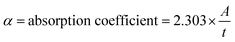
Using Tauc plots of (αhν)2 versus photon energy (hν), we figured out the optical bandgap (Eg) of the graphene–silicon (Gr–Si) composites from the UV-vis absorption data. We assumed that the electronic transition was allowed directly. We figured out the absorption coefficient (α) from the measured absorbance and we extended the linear part of each (αhν)2 curve to meet the energy axis at (αhν)2. This technique is frequently utilized for graphene-based semiconductors and thin-film hybrid materials.22,24 The optical bandgap energy (Eg) was calculated using Tauc's relation,32 as given below:
where
(
A = absorbance and
t = thickness),
33 t = thickness,
34 hν = photon energy,
Eg = optical bandgap energy,
A = constant, and
n = a constant that can take different values depending on the type of electronic transition.
Fig. 6(a)–(d) show the absorbance spectra and Tauc plots for the Gr 85% + Si 15%, Gr 80% + Si 20% and Gr 75% + Si 25% composites. The optical bandgaps were extracted by linear extrapolation of (αhν)2 versus photon energy, yielding values of 1.25 eV, 1.50 eV and 1.56 eV for increasing silicon content. This method is consistent with established graphene–silicon hybrid semiconductor studies. So, as the silicon content goes from 15 wt% to 25 wt%, the optical bandgap goes from 1.25 eV to 1.56 eV. This shows that adding Si is a good way to change the electronic structure of Gr–Si hybrid systems.
The gradual rise in Eg with Si loading is due to changes in the graphene π-electron network caused by silicon atoms and Si–O–C interfacial bonding. Adding Si creates localized electronic states and partial sp2 → sp3 rehybridization, which breaks up π-band delocalization and creates a finite bandgap. Similar mechanisms for widening the bandgap have been found in silicon-doped graphene, where Si 3p orbitals interact with graphene π-states to create energy levels that depend on the composition.35,36 These studies demonstrate that Si doping or Si–C hybridization can alter optical absorption edges, generate mid-gap states and enhance the effective bandgap via structural distortion and symmetry breaking.
3.4. Thermal analysis (TGA-DSC)
The thermogravimetric profiles in Fig. 7(b) show three areas where all the samples lost mass. Thermal stability was evaluated based on the degradation onset temperature and residual mass behavior rather than total mass loss. Although the Si-rich composite exhibits higher total mass loss due to silicon oxidation, the delayed onset of major degradation and formation of protective Si–O–C networks indicate enhanced thermal resistance at elevated temperatures. However, the Gr–Si composites show a small increase in mass (1–3%) below 200 °C, especially in the Si-rich samples from this study, which has been reported to be due to oxidation of Si particles and taking up of oxygen at early stages.37 This anomaly is due to the early oxidation of silicon particles and Si–O–C domains that are on the surface when there is oxygen in the air. A gradual decline means that the remaining organic groups are oxidizing, and the oxygen-containing groups C–O, C![[double bond, length as m-dash]](https://www.rsc.org/images/entities/char_e001.gif) O, and Si–O–C are breaking down. It is shown that adding Si improves thermal passivation by creating silica-like shells at the interface. Above 700 °C, the carbon lattice breaks down and Si turns into SiO2 in the air, which causes a sharp weight loss of 10–15%. This shows that adding more silicon makes the material more thermally stable. Fig. 7(a) shows the differential scanning calorimetry (DSC) curves of graphene–silicon (Gr–Si) composites taken in air from room temperature to 1200 °C. The wide endothermic region below 300 °C is where moisture is released, and surface species break down. The successive exothermic peaks at higher temperatures (500–850 °C) are where defective carbon is oxidized and Si–O–C and SiO2 networks are formed. Fig. 7(c) shows derivative DSC curves (heat-flow rate versus temperature). There are several exothermic maxima between 500 °C and 850 °C, which correspond to the oxidation of carbon domains in order and the restructuring of the Si–O–C network. The Si-rich composite (Gr 75:Si 25) has the sharpest and most temperature-shifted exothermic peak, which shows that the protective SiO2 passivation layer that forms at the interface makes the material more thermally stable and slows down the start of oxidation.38
O, and Si–O–C are breaking down. It is shown that adding Si improves thermal passivation by creating silica-like shells at the interface. Above 700 °C, the carbon lattice breaks down and Si turns into SiO2 in the air, which causes a sharp weight loss of 10–15%. This shows that adding more silicon makes the material more thermally stable. Fig. 7(a) shows the differential scanning calorimetry (DSC) curves of graphene–silicon (Gr–Si) composites taken in air from room temperature to 1200 °C. The wide endothermic region below 300 °C is where moisture is released, and surface species break down. The successive exothermic peaks at higher temperatures (500–850 °C) are where defective carbon is oxidized and Si–O–C and SiO2 networks are formed. Fig. 7(c) shows derivative DSC curves (heat-flow rate versus temperature). There are several exothermic maxima between 500 °C and 850 °C, which correspond to the oxidation of carbon domains in order and the restructuring of the Si–O–C network. The Si-rich composite (Gr 75:Si 25) has the sharpest and most temperature-shifted exothermic peak, which shows that the protective SiO2 passivation layer that forms at the interface makes the material more thermally stable and slows down the start of oxidation.38
 |
| | Fig. 7 (a) DSC, (b) TGA and (c) derivative DSC thermograms of graphene–silicon composites showing initial mass gain due to silicon oxidation and enhanced thermal stability with higher Si content. | |
3.5. FTIR analysis
Fig. 8 shows the FTIR spectra of Gr–Si composites with different compositions (Gr 85% + Si 15%, Gr 80% + Si 20% and Gr 75% + Si 25%). It shows that the surface functionalization changes significantly as the silicon content goes up. Normalized FTIR peak intensities reveal a systematic increase in CO and C–O vibrational modes with increasing silicon content, indicating enhanced oxidation and interfacial bonding. This trend supports bandgap widening via localized electronic states and partial sp2 → sp3 rehybridization. The peak at about 3066 cm−1, which corresponds to aromatic C–H stretching, is the same in all three samples. This shows that the sp2 carbon domains in the graphene are still there.39 The CO stretching peak at about 1755 cm−1 gets stronger as the amount of silicon increases. This means that more oxidation is happening and more carboxyl and ester groups are forming. As more silicon is added, the C–O stretching peak at 1180 cm−1 gets stronger. This means that there are more oxygenated functional groups.40 The peak around 2407 cm−1, which is due to OCO stretching, is stronger in the Gr 80% + Si 20% composite. This means that samples with moderate silicon content can hold more CO2.41 The FTIR spectrum shows a peak at 667 cm−1 that is usually linked to C–Br stretching or O–H bending in alcohols or phenols. It shows that there is either a carbon–bromine bond or a hydroxyl group, which gives us information about the material's chemical makeup.42 The Si–O bond, which is usually seen around 512 cm−1, is not very clear in the FTIR spectra. So, these samples don't show any clear signs of Si–O bonding. Also, as the amount of silicon increases, the amount of oxidation, oxygen functionalities and Si–O bonding increase. This makes the bandgap wider and the conductivity lower. The Gr 75% + Si 25% composite (S3) has the most oxidation and the biggest bandgap.43,44 The functional groups and chemical bonding of the tested samples are noted in Table 3.
 |
| | Fig. 8 FTIR spectra of graphene–silicon composites with varying compositions (Gr 75%–Si 25%, Gr 80%–Si 20% and Gr 85%–Si 15%), recorded over the range 400–3700 cm−1, illustrating the characteristic vibrational bands associated with Gr–Si interactions and confirming composition-dependent variations in functional group contributions and bonding environments. | |
Table 3 Comparison of the functional groups and chemical bonding of the tested samples
| Sample name |
Peak position wavenumber [cm−1] |
Functional groups |
Class |
Peak details |
| S1 |
3633 |
O–H (free) (alcohol/phenol) |
Alcohol, phenol |
Strong, sharp |
| 3062 |
C–H (aromatic) |
Aromatic hydrocarbon |
Medium to weak |
| 2356 |
OCO |
Carbonyl |
Strong absorption |
| 2938 |
N–H (amine salt) |
Amine salt |
Strong, broad |
| 1770 |
CO |
Ester, aldehyde |
Strong, sharp |
| 1527 |
N–O |
Nitro compound |
Medium |
| 1299 |
C–O |
Alcohol, ether |
Strong, sharp |
| 968 |
CC |
Alkene |
Medium |
| 581 |
C–I |
Halo compound |
Strong, sharp |
| 609 |
C–Br |
Halo compound |
Strong |
| S2 |
3409 |
N–H stretching |
Primary amine |
Medium |
| 2969 |
C–H stretching |
Alkane |
Medium |
| 2337 |
OCO |
Carbon dioxide |
Strong, sharp |
| 1677 |
C–H bending |
Aromatic compound |
Medium |
| 1369 |
O–H bending |
Alcohol |
Medium |
| 1068 |
C–N stretching |
Amine |
Strong |
| 647 |
C![[triple bond, length as m-dash]](https://www.rsc.org/images/entities/char_e002.gif) C stretching C stretching |
Alkene |
Medium |
| 497 |
C–Cl stretching |
Alkyl chloride |
Strong, sharp |
| S3 |
3629 |
O–H (free) (alcohol/phenol) |
Alcohol, phenol |
Strong, broad |
| 3054 |
C–H (aromatic) |
Aromatic hydrocarbon |
Medium to weak |
| 2356 |
OCO |
Carbonyl |
Strong absorption |
| 2938 |
N–H (amine salt) |
Amine salt |
Strong, broad |
| 1758 |
CO |
Ester, aldehyde |
Strong, sharp |
| 1515 |
N–O |
Nitro compound |
Medium |
| 1153 |
C–O |
Alcohol, ether |
Strong, sharp |
| 964 |
CC |
Alkene |
Medium |
| 513 |
C–I |
Halo compound |
Strong |
| 609 |
C–Br |
Halo compound |
Strong |
3.6. FESEM analysis
FESEM was employed to study the surface morphology and microstructural evolution of the Gr–Si composites. Fig. 9(a) depicts the microstructure of a 15% Si addition, characterized by smooth, wrinkled graphene sheets that create a continuous conductive network, interspersed with a limited number of finely dispersed Si nanoparticles. Fig. 9(b) shows the enlarged graphene area where the lamellar carbon layers tightly overlap, which makes sure that there are few defect sites and abundant electrical connectivity. This morphology will allow for metallic-like conduction with an optical band gap of about 1.25 eV. The homogeneous texture with low surface roughness also shows that the sheets stick together well and that Si does not fully agglomerate. This confirms that graphene keeps its natural two-dimensional continuity and high carrier mobility even when Si concentration is low.4 This gets rough and grainy, with Si clusters evenly spread out throughout the graphene matrix. In the same way, the area marked in Fig. 9(b) had Si clusters inside the graphene flakes and the interfacial Si–O–C zones from partial oxidation and bonding between Si and C atoms during thermal processing are shown in Fig. 9(c). The morphology suggests that silicon atoms are partially integrated into the graphene framework, resulting in defect states at the interfaces and localized energy levels.
 |
| | Fig. 9 Field emission scanning electron microscopy images of graphene + silicon composites of (a) Gr 85% + Si 15%, (b) Gr 80% + Si 20% and (c) Gr 75% + Si 25%. | |
The presence of conductive graphene and semiconducting Si–O–C domains elucidates the intermediate bandgap (1.50 eV) identified in UV-vis/Tauc analysis. Similar hybrid interfaces have been documented to enhance charge separation and photocarrier longevity in graphene–Si composites.45,46 Fig. 9(c) shows that the FESEM images of the 25% Si sample are made up of big silicon granules and broken graphene sheets. This shows that Si is clumping together and graphene is less continuous. The Si–O–C-rich cluster zones show that oxidized silicon cores are surrounded by disordered carbon. This suggests that there is some phase separation and the formation of silica-like shells. The morphological transformation indicates a definitive shift from metallic graphene behavior to semiconductor-like performance, analogous to the findings in the Si-functionalized graphene systems reported by Xu et al.47
Table 4 presents the elemental composition of graphene–silicon composite samples with weight ratios of 85:15, 80:20, and 75:25, taken at magnifications of 1000×, 2000×, 50000× and 75000×. The table shows that C and O are the most common atomic elements in all of the samples, while Si is present in smaller amounts. The Gr 75% + Si 25% sample had the most carbon atoms (69.02 atom%), which means it had a lot of graphene in it. The amount of silicon atoms went down as the amount of graphene went up.
Table 4 Elemental analysis of graphene–silicon (Gr–Si) composite samples at different weight ratios
| Sample |
Element |
keV |
Mass (%) |
Sigma |
Atom (%) |
| Gr 85% + Si 15% |
C K |
0.277 |
52.31 |
0.30 |
60.60 |
| O K |
0.525 |
42.13 |
0.51 |
36.64 |
| Si K |
1.739 |
5.56 |
0.12 |
2.76 |
| Total |
|
100.00 |
|
100.00 |
| Gr 80% + Si 20% |
C K |
0.277 |
50.53 |
0.27 |
58.50 |
| O K |
0.525 |
45.44 |
0.50 |
39.50 |
| Si K* |
1.739 |
4.03 |
0.10 |
2.00 |
| Total |
|
100.00 |
|
100.00 |
| Gr 75% + Si 25% |
C K |
0.277 |
61.98 |
0.27 |
69.02 |
| O K |
0.525 |
35.80 |
0.48 |
29.93 |
| Si K* |
1.739 |
2.22 |
0.07 |
1.06 |
| Total |
|
100.00 |
|
100.00 |
Elemental identification based solely on FESEM contrast is insufficient. Therefore, EDX spectra were used to confirm compositional variations. It is noted that EDX is surface sensitive and semi-quantitative. Hence, measured silicon contents may differ from bulk precursor ratios due to exfoliation induced segregation, oxidation and spatial heterogeneity. Fig. 10(a)–(c) show the EDX spectra of Gr–Si composites with three different compositions. The spectra show characteristic elemental peaks for C Kα (0.28 keV), O Kα (0.52 keV), and Si Kα (1.74 keV). The spectra show that carbon, oxygen and silicon are all present in all of the samples, which proves that silicon was successfully hybridized into the graphene framework. The changes in relative intensity show changes in composition and shape that are in line with what FESEM shows. Fig. 10(a) shows that the 85% Gr + Si 15% sample with high carbon content (52 wt%) and moderate oxygen level (42 wt%) has a dominant continuous graphene matrix, with only a small amount of Si (5.6 wt%). This composition matches the smooth, conductive shape seen in FESEM and explains why the optical bandgap is the lowest (1.25 eV). Fig. 10(b) shows an 80% Gr + 20% Si spectrum with 50.53 wt% C, 45.44 wt% O, and 4.03 wt% Si. The Si percentage looks a little lower than in S1, but the higher oxygen content suggests that there is more interfacial oxidation and Si–O–C bonding. This agrees with the granular shape seen in FESEM for this sample. These oxidized domains create localized electronic states that make it harder for carriers to move around. This is consistent with the intermediate bandgap (1.50 eV) and the highest sheet resistance of the samples. The composition shows a transition zone where graphene sheets and Si–O–C regions are present at the same time, which makes the structure more disordered. Fig. 10(c) shows (Gr 75% + Si 25%) that the relative Si peak intensity goes up and the O Kα signal gets stronger. This suggests that Si oxidation and Si–O–C bond formation are both happening more quickly. The higher oxygen content (45 wt%) shows that there is more interfacial hybridization, which is in line with the granular texture seen in FESEM. These Si–O–C linkages create localized electronic states that partially open the bandgap (1.50 eV) and keep the conductivity at a moderate level. The compositional trend (C > O > Si) and the changes in the Si and O peaks show that Si–O–C interfaces are forming over time, which control the pathways for charge transport. There have been reports of similar behavior in graphene–silicon nanohybrids, where controlled Si oxidation and interfacial bonding change how well the materials work for both light and electricity (Fig. 11).48
 |
| | Fig. 10 Energy-dispersive X-ray spectra of graphene + silicon: (a) Gr 85% + Si 15%, (b) Gr 80% + Si 20% and (c) Gr 75% + Si 25% composites. | |
 |
| | Fig. 11 Four-point probe resistivity measurements of graphene–silicon (Gr–Si) composites: (a) sheet resistance (Rs) and conductivity (σ) versus silicon content and (b) graphical correlation between bandgap (Eg) and electrical conductivity (σ). | |
Table 5 shows a summary of electrical conductivity and how it relates to the structure. Four-point probe measurements at room temperature indicate that conductivity diminishes as the optical bandgap expands from 1.25 eV (Gr 85% + Si 15%) to 1.56 eV (Gr 75% + Si 25%), which aligns with the gradual disruption of the π-conjugated graphene network due to Si incorporation. S1 (Gr 85%/Si 15%) has the lowest sheet resistance (8.179 kΩ; 1.223 S m−1) because FESEM shows that the graphene pathways are continuous and the Si is well-dispersed. S2 (Gr 80%/Si 20%) has the highest resistivity (9.678 kΩ; 1.033 S m−1) because the Si clusters are coarser, which stops percolation, and the Raman ID/IG is higher. S3 (Gr 75%/Si 25%) has the biggest bandgap, but it still regains some conductivity (8.867 kΩ; 1.128 S m−1) because graphene ribbons go around Si agglomerates and make new conductive networks. Similar to earlier research, adding Si to graphene broke up π-networks, raised the bandgap, and lowered the conductivity.49 These results, along with TGA/DSC evidence of silica-like passivation at high temperature, show that the quality of Si dispersion, not just the amount, controls the transport–bandgap trade-off in Gr–Si composites. This means that S1 can be used for contact/interconnect roles and S3 can be used for optoelectronic junctions where a wider gap with moderate conductivity is needed. Our findings for S1–S3 establish a correlation between the expanding band gap and diminishing conductivity in our Gr–Si composites.50
Table 5 Relationship between silicon content, bandgap modulation and electrical conductivity in graphene–silicon composites
| Nominal composition (Gr:Si) |
Bandgap Eg (eV) |
Sheet resistance Rs (kΩ) |
Conductivity σ (S m−1) |
| 85:15 |
1.25 |
8.179 |
1.223 |
| 80:20 |
1.50 |
9.678 |
1.033 |
| 75:25 |
1.56 |
8.867 |
1.128 |
3.7. Surface topography and particle analysis
Fig. 12 shows the analysis of the FESEM image application in Mountain 9, including surface topography, 3D views, and particles. The Gr 85% + Si 15% sample had very small particles, about 0.22–0.30 µm, and very large particles, with a perimeter of 900 µm and a low particle density of about 0.15 particles per mm2. These big groups made sharp height changes in the 3D surface model, which made the topography uneven, with isolated high peaks being the most common. The surface became much more even as Si rose to 20 wt%. The Gr 80% + Si 20% sample had a particle density of about 0.19–0.21 particles per mm2 and the range of particle sizes got smaller. The smallest features were still between 0.18 and 0.25 µm and the largest particles had a perimeter of only about 600–650 µm. The average size of the particles remained around 3.0–3.3 µm, which shows that the smaller particles were well-distributed. The corresponding 3D view showed a surface with a fine texture because there were a lot of moderate-height protrusions and no sudden changes in elevation, which is consistent with better dispersion. The particle density in the Gr 75% + Si 25% sample was about 0.18–0.20 particles per mm2, which is similar to the 20% Si composition. However, the particle size distribution was wider again.
 |
| | Fig. 12 3-D views, surface topography, and particle analysis of the composites: (a) Gr 85% + Si 15%, (b) Gr 80% + Si 20%, and (c) Gr 75% + Si 25%. | |
The smallest sizes were between 0.20 and 0.28 µm, and the biggest features had a perimeter of 720 to 780 µm. The average size went up to about 4.4–4.8 µm, which means that agglomeration happened again. The 3D topography showed wide, connected hills instead of separate peaks. The observation also showed that higher Si loading helps thicker and more connected surface domains grow. Overall, the best morphology was achieved at 20 wt% Si, because height distribution, along with particle size and density, was able to create the most stable and uniform surface structure.
4 Conclusions
This study introduces an innovative electrochemical exfoliation technique to manipulate the bandgap of graphene with regulated silicon integration, facilitating a distinct transition from semi-metallic to semiconducting properties. Graphene–silicon composites with composition dependent bandgaps ranging from 1.25 to 1.56 eV were synthesized. Silicon acts as an interfacial modulator, inducing π-network disruption through Si–O–C bonding and localized electronic states. The quality of silicon dispersion, rather than absolute silicon content, governs the trade-off between bandgap opening and electrical conductivity. This is because graphene has a natural limit of zero bandgap. Through extensive structural, morphological, thermal, optical, and electrical analyses, we establish for the first time a complete structure–bandgap–conductivity correlation for electrochemically exfoliated Gr–Si composites, providing new insights into how compositional tuning influences electronic state modulation.
The cold sintering and controlled electrochemical exfoliation fabrication method used here is a scalable way to get around the current material-level limits of graphene–silicon hybrids by making it possible to engineer the bandgap in a precise and repeatable way. XRD and Raman studies show that mid-gap defect states appear and graphitic crystallinity is disrupted as silicon content increases. UV-vis and Tauc analyses show that the bandgap widens depending on the composition, which is due to Si–O–C interfacial bonding and partial sp2 → sp3 rehybridization. The most important thing is that the quality of dispersion, not the amount of silicon, affects transport performance: graphene-rich composites (Gr85:Si15) have high conductivity and low defect densities, which makes them good for high-frequency interconnects. Intermediate compositions (Gr80:Si20) have higher sheet resistance because Si–O–C clusters and silicon-rich materials (Gr75:Si25) partially regain conductivity through secondary graphene networks while also being more thermally stable.
Thermal analysis has shown that all of these composites are very stable at high temperatures. Si-rich samples, on the other hand, showed the formation of a protective SiO2 passivation shell above 700 °C, which shows that they can be used in high-temperature devices. FESEM and EDX characterization studies further illustrate composition-dependent morphological evolution, wherein well-dispersed silicon nanoparticles facilitate coherent electron pathways at low Si loading and provoke agglomeration at elevated Si content, thereby enhancing bandgap widening through localized electronic state formation.
In general, and especially where tunable band gaps and controlled thermal stability are needed, these results show that Gr–Si composites are exciting materials for semiconductor, optoelectronic, and photovoltaic applications. So, the Gr75:Si25 composition is a good mix of semiconducting performance and moderate conductivity for optoelectronic junctions. Future research should concentrate on integrating density functional theory and molecular dynamics simulations to elucidate atomic-scale details regarding bandgap evolution and interfacial charge-transfer mechanisms.
Conflicts of interest
The authors declare no conflicts of interest.
Data availability
The data supporting this article is provided as part of the Supplementray information (SI). Supplementary information is available. See DOI: https://doi.org/10.1039/d5na01111f.
Acknowledgements
The authors would like to express their sincere thanks to Dhaka University of Engineering & Technology, Gazipur, Gazipur-1707, Bangladesh, for their important assistance and direction in finishing this research project.
References
- C. N. R. Rao, A. K. Sood, K. S. Subrahmanyam and A. Govindaraj, Graphene: the new two-dimensional nanomaterial, Angew Chem. Int. Ed. Engl., 2009, 48(42), 7752–7777, DOI:10.1002/anie.200901678.
- J. Jinschek, E. Yucelen, H. Calderon and B. Freitag, Quantitative atomic 3-D imaging of single/double sheet graphene structure, Carbon, 2011, 49, 556–562, DOI:10.1016/j.carbon.2010.09.058.
- M. J. Allen, V. C. Tung and R. B. Kaner, Honeycomb carbon: A review of graphene, Chem. Rev., 2010, 110(1), 132–145, DOI:10.1021/cr900070d.
- A. K. Geim and K. S. Novoselov, The rise of graphene, Nat. Mater., 2007, 6(3), 183–191, DOI:10.1038/nmat1849.
- A. K. Geim, Graphene: status and prospects, Science, 2009, 324(5934), 1530–1534, DOI:10.1126/science.1158877.
- Y. Zhang, Y.-W. Tan, H. L. Stormer and P. Kim, Experimental observation of the quantum Hall effect and Berry's phase in graphene, Nature, 2005, 438(7065), 201–204, DOI:10.1038/nature04235.
- E. Solati and D. Dorranian, Investigation of the Structure and Properties of Nanoscale Grain-Size beta-Tantalum Thin Films, Mol. Cryst. Liq. Cryst., 2013, 571, 67–76, DOI:10.1080/15421406.2012.741347.
- Ş. Ţălu, S. Solaymani, M. Bramowicz, N. Naseri, S. Kulesza and A. Ghaderi, Surface Micromorphology and Fractal Geometry of Co/CP/X (X= Cu, Ti, SM and Ni) Nanoflake Electrocatalysts, RSC Adv., 2016, 6 10.1039/C6RA01791F.
- Ş. Ţălu, M. Bramowicz, S. Kulesza, S. Solaymani, A. Shafiekhani, A. Ghaderi and M. Ahmadi, Gold Nanoparticles Embedded in Carbon Film: Micromorphology Analysis, J. Ind. Eng. Chem., 2015, 35 DOI:10.1016/j.jiec.2015.12.029.
- C. Lee, X. Wei, J. Kysar and J. Hone, Measurement of the Elastic Properties and Intrinsic Strength of Monolayer Graphene, Science, 2008, 321, 385–388, DOI:10.1126/science.1157996.
- K. Bolotin, et al., Ultrahigh Electron Mobility in Suspended Graphene, Solid State Commun., 2008, 146, 351–355, DOI:10.1016/j.ssc.2008.02.024.
- A. Balandin, et al., Superior Thermal Conductivity of Single-Layer Graphene, Nano Lett., 2008, 8, 902–907, DOI:10.1021/nl0731872.
- M. Bacon, S. J. Bradley and T. Nann, Graphene Quantum Dots, Part. Part. Syst. Charact., 2014, 31(4), 415–428, DOI:10.1002/ppsc.201300252.
- J. Shen, Y. Zhu, X. Yang and C. Li, ChemInform Abstract: Graphene Quantum Dots: Emergent Nanolights for Bioimaging, Sensors, Catalysis and Photovoltaic Devices, Chem. Commun., 2012, 48, 3686–3699, 10.1039/c2cc00110a.
- J. Zhang, et al., Strongly Green-Photoluminescent Graphene Quantum Dots for Bioimaging Applications, Chem. Commun., 2011, 47, 6858–6860, 10.1039/c1cc11122a.
- C. Zhu, J. Zhai and S. Dong, Bifunctional fluorescent carbon nanodots: Green synthesis via soy milk and application as metal-free electrocatalysts for oxygen reduction, Chem. Commun., 2012, 48, 9367–9369, 10.1039/c2cc33844k.
- Y. H. Lee, L. Polavarapu, N. Gao, P. Yuan and Q.-H. Xu, Enhanced Optical Properties of Graphene Oxide–Au Nanocrystal Composites, Langmuir, 2012, 28(1), 321–326, DOI:10.1021/la204047a.
- S. Bongu, P. Bisht, T. V. Thu and A. Sandhu, Multiple Nonlinear Optical Response of Gold Decorated-Reduced Graphene Oxide-Nanocomposite for Photonic Applications, Journal of Atomic, Molecular, Condensate and Nano Physics, 2015, 2, 207–214, DOI:10.26713/jamcnp.v2i3.346.
- M. M. Rana, M. A. Chowdhury, H. Aoyon, M. R. Khandaker and M. H. Hossain, Tunable Bandgap and Structural Characterization of Boron-Doped Graphene Synthesized through Electrochemical Exfoliation, Adv. Eng. Mater., 2025 DOI:10.1002/adem.202501514.
- T. Feng, et al., Efficiency enhancement of graphene/silicon-pillar-array solar cells by HNO3 and PEDOT-PSS, Nanoscale, 2012, 4(6), 2130, 10.1039/c2nr12001a.
- X. Miao, et al., High Efficiency Graphene Solar Cells by Chemical Doping, Nano Lett., 2012, 12, 2745–2750, DOI:10.1021/nl204414u.
- X. An, F. Liu, Y. Jung and S. Kar, Tunable Graphene-Silicon Heterojunctions for Ultrasensitive Photodetection, Nano Lett., 2013, 13(3), 909–916, DOI:10.1021/nl303682j.
- K. S. Novoselov, et al., Electric Field Effect in Atomically Thin Carbon Films, Science, 2004, 306(5696), 666–669, DOI:10.1126/science.1102896.
- C. Fu, C. Song, L. Liu, W. Zhao and X. Xie, High Reversible Silicon/Graphene Nanocomposite Anode for Lithium-Ion Batteries, Int. J. Electrochem. Sci., 2016, 11(1), 154–164, DOI:10.1016/S1452-3981(23)15833-0.
- H. Huang, The Effect of Commercialized Binders on Silicon Oxide Anode Material for HighCapacity Lithiumion Batteries, Int. J. Electrochem. Sci., 2016, 11, 8697–8708, DOI:10.20964/2016.10.29.
- L. Pevelen and D. Delphine, Small Molecule X-Ray Crystallography, Theory and Workflow, ed J. C. Lindon, Academic Press, 2010, pp. 2559–2576 Search PubMed.
- S. Fatimah, R. Ragadhita, D. F. A. Husaeni and A. Bayu Dani Nandiyanto, ASEAN Journal of Science and Engineering, 2022, 2, 65 CrossRef.
- D. J. Lim, N. A. Marks and M. R. Rowles, Carbon, 2020, 162, 475 CrossRef CAS.
- K. Krishnamoorthy, M. Veerapandian, R. Mohan and S.-J. Kim, Investigation of Raman and photoluminescece studies of reduced graphene oxide sheets, Appl. Phys. A, 2011, 106, 501–506, DOI:10.1007/s00339-011-6720-6.
- S. Dash, T. Dash and T. Rout, Preparation of graphene oxide by dry planetary ball milling technique under oxygen atmosphere, IOP Conf. Ser.:Mater. Sci. Eng., 2020, 872, 12180, DOI:10.1088/1757-899X/872/1/012180.
- M. Houmad, H. Zaari, A. Benyoussef, A. El Kenz and H. Ez-Zahraouy, Optical conductivity enhancement and band gap opening with silicon doped graphene, Carbon, 2015, 94, 1021–1027, DOI:10.1016/j.carbon.2015.07.033.
- P. R. Jubu, O. Adedokun, C. Mbakaan, A. Nathan-Abutu, E. Danladi, J. N. Tsaviv, P. I. Kyesmen, B. J. Akeredolu, A. T. Adepoju, F. Aungwa, Y. Yusof, O. S. Obaseki, Y. S. Elzawiei and M. Z. Pakhuruddin, J. Mater. Sci.: Mater. Electron., 2025, 36, 961 CrossRef CAS.
- T. Pandit, Absorbance and Transmittance Measurement of CsI Thin Films, 2013 Search PubMed.
- R. Rai and B. K. Singh, Absorbance and Transmittance Measurement of CsI Thin Films, 2013 Search PubMed.
- M. Shahrokhi and C. Leonard, Tuning the band gap and optical spectra of silicon-doped graphene: Many-body effects and excitonic states, J. Alloys Compd., 2017, 693, 1185–1196, DOI:10.1016/j.jallcom.2016.10.101.
- S. Sahu and G. C. Rout, Band gap opening in graphene: a short theoretical study, Int. Nano Lett., 2017, 7(2), 81–89, DOI:10.1007/s40089-017-0203-5.
- G. Ge, et al., Manipulating Oxidation of Silicon with Fresh Surface Enabling Stable Battery Anode, Nano Lett., 2021, 21(7), 3127–3133, DOI:10.1021/acs.nanolett.1c00317.
- C. Yin, X. Li, P. Chen, G. M. Kale and B. Zhu, Oxidation resistance and wettability of graphite/SiC composite, Int. J. Mater. Res., 2018, 109(7), 629–637, DOI:10.3139/146.111644.
- G. Surekha, K. V. Krishnaiah, N. Ravi and R. Padma Suvarna, FTIR, Raman and XRD analysis of graphene oxide films prepared by modified Hummers method, J. Phys.: Conf. Ser., 2020, 1495, 012012, DOI:10.1088/1742-6596/1495/1/012012.
- Y. Liang, D. Wu, X. Feng and K. Müllen, Dispersion of graphene sheets in organic solvent supported by ionic interactions, Adv. Mater., 2009, 21(17), 1679–1683, DOI:10.1002/adma.200803160.
- S. Saxena, T. A. Tyson, S. Shukla, E. Negusse, H. Chen and J. Bai, Investigation of structural and electronic properties of graphene oxide, Appl. Phys. Lett., 2011, 99(1), 013104, DOI:10.1063/1.3607305.
- N. Prabavathi and N. S. Nayaki, Experimental Spectroscopic (FT-IR, FT-Raman, NMR) and DFT Studies of 7-methoxy-4-bromomethylcoumarin, J. Environ. Nanotechnol., 2014, 3(2), 108–121, DOI:10.13074/jent.2014.03.142072.
- P. Shemella and S. K. Nayak, Electronic structure and band-gap modulation of graphene via substrate surface chemistry, Appl. Phys. Lett., 2009, 94(3) DOI:10.1063/1.3070238.
- C. V. Gomez, E. Robalino, D. Haro, T. Tene, P. Escudero, A. Haro and J. Orbe, Structural and Electronic Properties of Graphene Oxide for Different Degree of Oxidation, Mater. Today: Proc., 2016, 3(3), 796–802, DOI:10.1016/j.matpr.2016.02.011.
- L. K. Pillari, K. Lessoway and L. Bichler, Carbon nanotube and graphene reinforced magnesium matrix composites: A state-of-the-art review, J. Magnesium Alloys, 2023, 11, 1825–1905, DOI:10.1016/j.jma.2023.05.010.
- J. Lee, C. Lee, J. Jun, D. Shin and J. Jang, A metal-oxide nanofiber-decorated three-dimensional graphene hybrid nanostructured flexible electrode for high-capacity electrochemical capacitors, J. Mater. Chem. A, 2014, 2(30), 11922–11929, 10.1039/C4TA01695E.
- M. Houmad, H. Zaari, A. Benyoussef, A. Kenz and H. Ez-Zahraouy, Optical Conductivity enhancement and band gap opening With Silicon doped graphene Optical Conductivity enhancement and band gap opening With Silicon doped graphene, Carbon, 2015, 94, 1021–1027, DOI:10.1016/j.carbon.2015.07.033.
- M. Houmad, H. Zaari, A. Benyoussef, A. El Kenz and H. Ez-Zahraouy, Optical conductivity enhancement and band gap opening with silicon doped graphene, Carbon, 2015, 94, 1021–1027, DOI:10.1016/j.carbon.2015.07.033.
- C. Chen, et al., An insitu iodine-doped graphene/silicon composite paper as a highly conductive and self-supporting electrode for lithium-ion batteries, RSC Adv., 2017, 7(61), 38639–38646, 10.1039/C7RA06871A.
- M. M. Ervasti, Z. Fan, A. Uppstu, A. V Krasheninnikov and A. Harju, Silicon and silicon-nitrogen impurities in graphene: Structure, energetics, and effects on electronic transport, Phys. Rev. B:Condens. Matter Mater. Phys., 2015, 92(23), 235412, DOI:10.1103/PhysRevB.92.235412.
|
| This journal is © The Royal Society of Chemistry 2026 |
Click here to see how this site uses Cookies. View our privacy policy here. 
 Open Access Article
 This Open Access Article is licensed under a Creative Commons Attribution-Non Commercial 3.0 Unported Licence
 *a,
Md. Arefin Kowsera,
Mohammad Asaduzzanaman Chowdhurya,
Md. Masud Ranaa,
Hasanuzzaman Aoyona,
Abdul Ahadb,
Md. Abdulla Al Koraisa,
Tasnim Alam Sayedib,
Samsul Islama and
Md. Masud Khanb
*a,
Md. Arefin Kowsera,
Mohammad Asaduzzanaman Chowdhurya,
Md. Masud Ranaa,
Hasanuzzaman Aoyona,
Abdul Ahadb,
Md. Abdulla Al Koraisa,
Tasnim Alam Sayedib,
Samsul Islama and
Md. Masud Khanb


 .
.


 (A = absorbance and t = thickness),33 t = thickness,34 hν = photon energy, Eg = optical bandgap energy, A = constant, and n = a constant that can take different values depending on the type of electronic transition.


