DOI:
10.1039/D5NA01014D
(Paper)
Nanoscale Adv., 2026,
8, 1386-1399
Multipolar origin and polarization-controlled high-Q quasi-BIC Fano resonances in dielectric metasurfaces for sensing applications
Received
1st November 2025
, Accepted 6th January 2026
First published on 7th January 2026
Abstract
We designed a multifunctional all-dielectric metasurface employing cuboid structures patterned with bow-tie-shaped nanoholes; it exhibits multiple Fano resonances induced by quasi-bound states in the continuum (quasi-BICs) through structural asymmetry. Among them, several resonant modes demonstrated high quality factors in the range of 103–104, along with near-unity modulation depth and strong spectral contrast. The optical responses were analyzed utilizing the finite-difference time-domain (FDTD) method, with Fano profiles fitted to theoretical models and the BIC-governed modes validated via the inverse-square ratio law. Furthermore, multipolar decomposition and electromagnetic spatial field profiles revealed the origins of the resonance, while LC circuit modeling provided additional physical insight into the Fano profiles. The proposed metasurface also exhibited strong polarization dependence, indicating its potential for active optical switching. Finally, the refractive-index sensing performance, including the potential for detecting Vibrio cholerae in an appropriate environment, reached a sensitivity of 342 nm per RIU and a figure of merit of 217.14 RIU−1. Advancing the control of high-Q quasi-BIC Fano resonances, this study highlights Fano resonators’ potential for refractive-index sensing and active switching.
1 Introduction
Metasurfaces with engineered strong light–matter interactions enable advanced and multifunctional control over optical wavefronts, including amplitude, phase, polarization, and dispersion.1–5 Their compactness, high design flexibility, and ability to integrate with existing platforms make them ideal candidates for next-generation technologies in flat optics, compact imaging, on-chip photonic circuits, and broadband optical communication.6–8 By harnessing the sharp spectral features arising from resonant effects, such as Fano resonances and bound states in the continuum (BICs), these planar photonic structures provide exceptional capability for light manipulation at subwavelength scales.9–12 This ability depends critically on the material’s inherent optical characteristics and the precise engineering of resonant nanostructures. Metasurfaces are broadly categorized into plasmonic and all-dielectric types, each distinguished by their resonance mechanisms and electromagnetic response.13 Plasmonic metasurfaces, typically composed of noble metals or graphene, rely on localized surface plasmon resonances to achieve strong near-field confinement in the visible to near-infrared range.14,15 However, their practical utility is constrained by inherent ohmic losses, which limit Q factors and degrade performance in applications requiring high spectral selectivity.16 Notably, all-dielectric metasurfaces constructed from high-refractive-index materials, such as silicon, germanium and gallium phosphide, support low-loss Mie resonances and enable the excitation of high-Q modes, including BICs, through careful control of geometric and symmetry parameters. These structures exhibit minimal absorption losses and enhanced field confinement, and are compatible with CMOS fabrication processes, making them particularly attractive for scalable and low-loss photonic integration.17–19
Among the various multipolar excitations in nanophotonics, the toroidal dipole (TD), first introduced by Zeldovich in 1957, has emerged as a distinctive mode arising from closed-loop displacement currents, representing a unique excitation in all-dielectric metasurfaces, with weak radiation and behavior markedly different from conventional electric (ED) and magnetic dipole (MD) responses.20 Although TD modes were previously overlooked due to masking by dominant multipoles, recent studies have demonstrated that their excitation can be selectively enhanced through structural asymmetry, near-field coupling, and engineered high-index dielectric arrays.21,22 These configurations support a high Q factor with suppressed radiative loss, making them promising for applications in sensing and nonlinear optics. However, the relatively weak near-field confinement of TD modes highlights further optimization in geometry and materials design to maximize their photonic functionality.
Ultra-narrow optical resonances with exceptionally high Q factors and minimal losses play a vital role in modern nanophotonics, enabling enhanced light–matter interactions essential for applications such as high-sensitivity sensors, nonlinear optics, slow-light devices, narrowband absorbers, and spectral filters.4,23–27 A common route to achieving such resonances is through Fano resonance, resulting from interference between radiative and non-radiative modes, producing sharp asymmetric line shapes.28,29 This effect becomes particularly pronounced when combined with BICs, arising from non-radiating localized states embedded within the continuous radiation spectrum.30 Although ideal BICs possess infinite Q factors and zero linewidth, practical implementation is achieved through quasi-BICs, where slight structural asymmetry induces weak coupling to free-space radiation, resulting in finite but extraordinarily high Q factors.31–34 Such mechanisms have been widely utilized to excite high-Q TD Fano resonances in all-dielectric metasurfaces.35 Pang et al. introduced square defects into Si tetramer arrays to realize polarization-independent quasi-BICs.36 Sun et al. employed a nanorod–ring unit with broken symmetry, enabling tunable TD resonances by varying the nanorod length.35 Li et al. achieved BIC-governed high-Q resonances in a Si-based hollow metasurface by incorporating asymmetric air holes.22 Additionally, Lv et al. investigated quadrupolar quasi-BICs in GaP nanodisk arrays activated via lateral displacement.13 However, beyond geometric asymmetry, this effect can also be realized through material asymmetry. Yu et al. demonstrated dual-band, polarization-insensitive TD modes using permittivity-asymmetric Si–InAs cuboid tetramers.37 Although GaP exhibits a high refractive index comparable to Si, comprehensive investigations of GaP-based metasurfaces, especially regarding BIC-governed Fano resonances, remain lacking. Moreover, hollow-structured GaP metasurfaces tailored for such resonance phenomena have yet to be thoroughly explored.
In this paper, we present an all-dielectric metasurface exhibiting multiple Fano resonances in the near-infrared (NIR) regime, predominantly governed by MD and TD excitations. The incorporation of structural asymmetry—achieved by modifying both the dimension and orientation of a single triangular nanohole of bow-tie-shaped nanoholes—introduced quasi-BIC-supported Fano resonances, resulting in additional pronounced Fano resonances. These resonances exhibited both exceptionally high quality factors and modulation depths. The Fano profiles for both symmetry and asymmetry configurations were fitted using the theoretical model, while the BIC mode was validated by calculating the inverse-square ratio law. Additionally, the Fano resonances were interpreted using an equivalent LC circuit model to elucidate the underlying resonance mechanism. To further analyze the origin of resonance, the contributions of various multipolar moments were investigated through spatial distributions of the electric and magnetic fields. The impact of the polarization angle on optical performance was investigated, demonstrating potential for being utilized as an optical switch. Moreover, the impact of the structural parameters was also investigated. Finally, the sensing capability of the structure was assessed by changing the ambient refractive index to simulate the presence of Vibrio cholerae. This all-dielectric metasurface, with lower complexity in design, offers promising prospects for advanced applications in refractive index (RI) sensing and active photonic switching.
2 Structure design and methodology
Fig. 1(a) depicts our proposed all-dielectric metasurface, comprising a two-dimensional periodic array of GaP nanocuboids with a square cross-section and bow-tie-shaped nanoholes, deposited on a SiO2 substrate along the x and y axes with a periodicity P = 650 nm.
 |
| | Fig. 1 (a) 3D schematic illustration of the proposed all-dielectric bow-tie-etched metasurface; (b) x–y and (c) x–z plane view of the structure. The optimized structural parameters: P = 650 nm, w = 550 nm, tSiO2 = 200 nm, tGaP = 150 nm, and δ = s2 – s1. (d) Optical simulation configuration of the proposed structure. | |
The thickness of the substrate was considered to be tSiO2 = 200 nm. Moreover, Fig. 1(b) and (c) present the cross-sectional views along the xy- and yz-planes, respectively. The side of the square-shaped cross-section of the GaP nanocuboids was w = 550 nm, while the thickness was tGaP = 150 nm. The bow-tie-shaped nanoholes were comprised of two equilateral triangles with side lengths s1 and s2, separated from center to center with a distance of 275 nm. To facilitate the BIC, an asymmetry parameter δ was introduced, defined as δ = s2 – s1. The complex refractive index of GaP and SiO2 were adopted from Bond et al.38 and Palik et al.,39 respectively; see the SI for details.
We employed the finite-difference time-domain (FDTD) approach in Ansys Lumerical to quantitatively investigate the optical properties of our proposed structure. The simulation configuration is illustrated in Fig. 1(d). Since our proposed metasurface exhibited periodicity along the x and y axes, we employed periodic boundary conditions to reduce the computational space and simulation time while applying 12-layer perfectly matched layer (PML) boundary conditions along both directions of the z-axis to eliminate parasitic reflections from the structure. An additional mesh with dimensions 4 nm × 4 nm × 4 nm was incorporated for precise simulation. The simulation was conducted by considering the structure immersed in a liquid medium, such as water, with a refractive index of 1.33 at a temperature of 300 K. A CW-normalized plane-wave source was positioned incident from the top of the structure with the wavelength ranging from 900 nm to 1600 nm. We employed a frequency-domain field and power monitor beneath the structure to quantify the transmittance T(λ), which is the ratio of the transmitted power, PT(λ), to the incident power, PI(λ), expressed as follows:4
| |  | (1) |
3 Results and discussion
3.1 Dimensional asymmetry
The asymmetry in the dimensions of the bow-tie-shaped nanoholes allowed our proposed structure to exhibit resonances governed by the BIC. Fig. 2(a) illustrates the transmittance spectra of the structure for δ = 0 nm (s1 = s2 = 130 nm) and δ = 100 nm (s1 = 130 nm, s2 = 230 nm).
 |
| | Fig. 2 (a) Transmittance spectra of our proposed structure for δ = 0 nm and 100 nm. Plot of FDTD-calculated and fitted graphs for (b) δ = 0 nm near λ = 1044 nm and 1217 nm, and (c) δ = 100 nm near λ = 911 nm, 1159 nm and 1278 nm under TM-polarized incident light. (d) Schematics of the LC circuit models for Mode I and II (δ = 0 nm). (e) FDTD-calculated and fitted curves with the LC circuit for Mode I and II, for δ = 0 nm. | |
When δ = 0 nm, the structure maintained a distinct in-plane symmetry, resulting in two sharp Fano profiles at λ = 1044 nm (Mode I), and 1217 nm (Mode II). The structure also supported symmetry-protected BICs with theoretically infinite Q factors, but they remained undetectable in the transmittance spectrum. Moreover, we analyzed the finite-size effects of the structure (20 × 20 array) for this configuration, which resulted in broader but qualitatively consistent resonance behavior; see the SI for details. However, the in-plane symmetry was disrupted when we considered δ = 100 nm, allowing the non-radiative bound states to couple with the free-space continuum and access the radiation channel.22 Consequently, the radiation channel transformed into a resonant mode, allowing energy leakage and outward radiation, which led to the transformation of symmetry-protected BICs into quasi-BICs.13 Therefore, we observed three additional Fano-profile resonances at λ = 911 nm (Mode III), 1159 nm (Mode IV), and 1278 nm (Mode V) governed by quasi-BICs. Meanwhile, Mode I and II in the Fano profile of this structure experienced a blue-shift to λ = 1036 nm and 1195 nm, respectively.
The performance of the metasurface in optical applications can be evaluated based on the modulation depth, spectral contrast ratio, and Q-factor of the Fano resonance. The modulation depth is defined by:37
| | 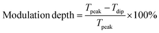 | (2) |
where
Tpeak and
Tdip are the maximum and minimum values of the transmittance spectrum, respectively. Moreover, we calculated the spectral contrast ratio by utilizing these two parameters:
| | 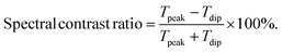 | (3) |
To consider the transmittance spectra qualitatively, the Fano model can be expressed as:
| | 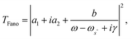 | (4) |
where
a1,
a2, and
b are the real number constants,
ωs° and
ω are the resonance and angular frequency, and
γ is the overall damping loss. The radiative
Q-factor,
Qrad, can be defined as
Qrad =
ωs°/2γ. We employed
eqn (4) to fit the calculated Modes I and II for
δ = 0 nm and III to V for
δ = 100 nm.
Fig. 2(b) and (c) present the calculated and fitted Fano profiles for
δ = 0 nm (Mode I and II) and for 100 nm (Mode III to V), demonstrating that the fitted curve closely aligns with the calculated data.
Table 1 summarizes the extracted
Qrad values from these fittings, modulation depth, and spectral contrast ratio for Modes I and II (
δ = 0 nm) and I–V (
δ = 100 nm).
Table 1 Extracted values of quality factor, modulation depth, and spectral contrast ratio for Modes I and II (δ = 0 nm) and III–V (δ = 100 nm)
|
δ
|
Mode |
Quality factor (Qrad) |
Modulation depth (%) |
Spectral contrast ratio (%) |
| 0 nm |
I |
2.90 × 10² |
99.93 |
99.87 |
| II |
1.10 × 10² |
99.78 |
99.57 |
| 100 nm |
I |
6.14 × 10² |
74.51 |
59.39 |
| II |
1.54 × 10² |
99.95 |
99.89 |
| III |
3.17 × 10³ |
98.50 |
97.04 |
| IV |
8.96 × 101 |
99.50 |
99.00 |
| V |
6.38 × 10⁴ |
47.15 |
30.85 |
A simplified LC circuit based on the stable-input impedance mechanism can be employed to replicate the Fano resonance profile. Introducing a capacitor or an inductor in parallel with the LC circuit enables coupling between a broadband bright mode and a narrowband dark mode, thus giving rise to an asymmetric Fano-like resonance.40Fig. 2(d) depicts the LC circuit representations for Modes I and II (δ = 0 nm), where a complementary capacitor and inductor were incorporated for Modes I and II, respectively. The corresponding stable-input impedances of these configurations are as follows:
| | 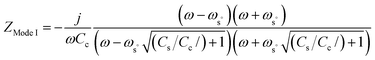 | (5) |
| | 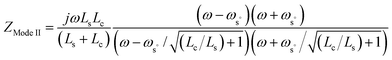 | (6) |
Here, j is the imaginary unit, Ls and Cs denote the series inductor and capacitor, while Lc and Cc represent the complementary inductor and capacitor, respectively. We can define transmittance as the ratio of incident power (Pinput) to transmitted power (Poutput). Fig. 2(e) depicts both the LC-circuit-fitted and calculated Modes I and II (δ = 0 nm), demonstrating a good match between the fitted data and the calculated result; see the SI for details.
Fig. 3(a) provides further insight into the formation of symmetry-breaking quasi-BIC-supported Fano resonance profiles by illustrating the transmittance spectra for δ = 0 nm to 125 nm. At δ = 0 nm, the transmittance spectrum exhibited three symmetry-protected BICs with a theoretically infinite Q-factor. When δ ≠ 0 nm, the in-plane symmetry was broken, leading to the appearance of three distinct Fano profiles (Mode III to V) supported by symmetry-breaking quasi-BICs. At δ = 25 nm, we found these resonances at λ = 921 nm, 1198 nm, and 1299 nm, while at δ = 125 nm, these resonances experienced a blue-shift to λ = 911 nm, 1159 nm, and 1278 nm, respectively. Moreover, Modes I and II exhibited a blue-shift, similar to the discussion in the previous section. These blue-shifts resulted from the decrease in the effective refractive index of the metasurface with the increase in the asymmetry degree α. Here, α represents normalized perturbation, defined as the ratio of ΔA to A, where ΔA and A represent the area of the broken part (i.e., reduced area due to symmetry breaking (δ ≠ 0 nm) of the bow-tie shaped nanohole) and the GaP-based dielectric part, respectively. Here, we adopted the normalized perturbation since it quantifies the fractional modification of the GaP dielectric region rather than a single structural displacement. Moreover, the Qrad experienced a decrease with the increase in α, resulting from the wider radiation channel, which gave rise to more energy loss through radiation. Fig. 3(b) and (c) illustrate the extracted Qrad as a function of α for Modes III and IV, which maintained the inverse-square ratio law Qrad ∝ (α)−2. This trend satisfied the fundamental criterion for a symmetry-protected BIC, indicating that the Fano resonance was governed by the BIC. This linear relation resulted from the incorporated α, which represented multiple geometric contributions simultaneously, rather than the actual symmetry-breaking perturbation.
 |
| | Fig. 3 (a) Transmittance spectra for different asymmetry parameters, δ = 0 nm to 125 nm, under TM-polarized incident light; (b) and (c) relationship between the Q-factor, Qrad, and the degree of asymmetry α for Mode III and IV, respectively. α was defined by the ratio of ΔA and A. The solid red line represents the fitted data, indicating an inverse-square relationship between the Qrad and α. Additionally, the inset of (b) highlights the magnitude of ΔA, denoted by the marked red region. | |
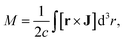
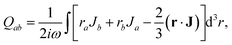
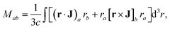
The underlying physical mechanism responsible for the emergence of Fano resonances can be elucidated through multipole decomposition. This method resolves the total response into distinct contributions, including the electric dipole (ED), magnetic dipole (MD), electric quadrupole (EQ), magnetic quadrupole (MQ), and toroidal dipole (TD). The moments of these are mathematically defined as:13
| |  | (7) |
| |  | (8) |
| |  | (9) |
| |  | (10) |
| |  | (11) |
where
J,
r, and
c represent the current density, displacement vector, and speed of light, respectively, while
a and
b denote the Cartesian tensor components.
Fig. 4(a) presents the 3D schematics of the ED, MD, and TD modes. The corresponding scattering power contributions of each multipole (ED, MD, TD, EQ and MQ) for the case of δ = 0 nm are shown in Fig. 4(b). As observed, at a distinct resonance wavelength, a specific multipolar component dominated the scattering response. Specifically, Mode I exhibited a dominant MD contribution, while Mode II was primarily influenced by the TD response. Consequently, the electromagnetic field distribution was primarily governed by the strongest dipolar excitation. Fig. 4(c) and (d) show the spatial distributions of the electric and magnetic fields at λ = 1044 nm, while Fig. 4(e) and (f) correspond to λ = 1217 nm.
 |
| | Fig. 4 (a) 3D schematic representation of ED, MD, and TD modes. (b) Scattering power contributions from individual multipole moments—namely ED, TD, MD, EQ, and MQ—for the proposed structure at δ = 0 nm, where the red-shaded regions highlight resonant Modes I and II. Spatial distribution of electric and magnetic fields in the x–y plane (c and d) at λ = 1044 nm and (e and f) at λ = 1217 nm. White arrows indicate the orientation of the corresponding field vectors. | |
At λ = 1044 nm, the magnetic field distribution in the xy-plane featured two oppositely circulating loops, which drove an anticlockwise vortex of the electric field in the xz-plane. This configuration reflects the dominant influence of MD excitation at this resonance, oriented in the negative y direction. In contrast, at λ = 1217 nm, the electric field assumed a similar looped structure in the xy-plane, while the magnetic field exhibited a clockwise vortex in the yz-plane, revealing the dominance of TD excitation at this resonance in the positive x direction. For δ = 100 nm, a pronounced TD excitation was identified at λ = 911 nm, whereas MD excitation was found to dominate at λ = 1159 nm and λ = 1278 nm; see the SI for details.
3.2 Rotational asymmetry
The rotation of an individual triangular nanohole introduces in-plane symmetry breaking within our proposed structure. To examine this effect, we investigated the rotational dependence of a single nanohole in our structure with δ = 0 nm, rotating from 0° to 360°. As shown in Fig. 5(a), Mode I remained at λ = 1044 nm throughout the entire rotation range, indicating its robustness to rotational asymmetry.
 |
| | Fig. 5 (a) Transmittance spectra of the proposed structure, incorporating rotational asymmetry (one triangular nanohole rotated from 0° to 360°, as in the figure). (b) Scattering power contributions from individual multipole moments at the rotation of 180°. (c) Electric and magnetic field distribution profile for λ = 1201 nm at 180°. | |
In contrast, Mode II red-shifted from λ = 1217 nm to λ = 1221 nm as the rotation increased from 0° to 180°. Upon further rotation to 360°, Mode II gradually blue-shifted, ultimately returning to its original resonance wavelength at λ = 1217 nm. Meanwhile, an additional resonance was observed near Mode II with the rotation of this single nanohole. At a rotation angle of 90°, this resonance emerged at λ = 1207 nm with a modulation depth of 46.46%. As the nanohole rotated further to 180°, the resonance exhibited a blue-shift to λ = 1201 nm, accompanied by a significantly enhanced modulation depth of 93.53%. The corresponding Qrad was 9.86 × 10² at both 90° and 270°, but decreased to 4.40 × 10² at 180°. The observed blue-shift and Qrad reduction with increasing asymmetry suggest that this resonance originated from a quasi-BIC. To further elucidate the origin of the additional Fano resonance, the scattering power contributions from individual multipole moments were analyzed for a rotational angle of 180°. As shown in Fig. 5(b), the resonance at λ = 1201 nm is predominantly governed by the MD, EQ, and MQ modes. This interpretation is further supported by the electric and magnetic field distributions in Fig. 5(c), where two anti-clockwise and one clockwise loops in the electric field confirm the coexistence of MD and EQ characteristics. Additionally, the localized out-of-plane magnetic field excitation indicates a strong presence of MD and MQ contributions.
3.3 Impact of light polarization
Owing to the asymmetric configuration of the proposed structure, we analyzed its optical response under varying polarization angles, φ, of the incident light. The analysis was carried out for φ ranging from 0° to 90°, considering structural asymmetries of δ = 0 nm and 100 nm. The corresponding transmittance spectra are shown in Fig. 6(a) and (b). For δ = 0 nm, Mode I maintained its resonance wavelength and modulation depth, though its Q-factor decreased to 1.38 × 10². In contrast, Mode II exhibited a gradual reduction in modulation depth with increasing φ, and fully vanished at φ = 90°. Interestingly, a new Fano profile emerged at λ = 1175 nm as φ increased, characterized by a Q-factor of 4.34 × 10² and a modulation depth of 99.96% at φ = 90°. Fig. 6(c) illustrates the transmittance at λ = 1175 nm, and 1217 nm for φ = 0° to 360°, presenting the obvious on–off state of the corresponding resonance modes. For δ = 100 nm, all Fano profiles except Mode I exhibited a gradual reduction in modulation depth with increasing φ, and totally disappeared at φ = 90°. However, four new Fano profiles started to appear with the increase in φ. At φ = 90°, new four Fano profiles were found at λ = 936 nm, 1012 nm, 1030 nm, and 1148 nm with modulation depths of 73.06%, 26.64%, 80.07%, and 98.21%, respectively. The Q-factors of these four Fano profiles were 4.70 × 10³, 2.95 × 10³, 6.64 × 10², and 1.73 × 10³, respectively. The transmittance at these particular wavelengths is shown in Fig. 6(d) for φ = 0° to 360° to clearly present the on–off state. The aforementioned characteristics of both structures with δ = 0 nm and 100 nm allow them to be utilized as an active optical switch.
 |
| | Fig. 6 Transmittance spectra for (a) δ = 0 nm, and (b) δ = 100 nm at polarization angles φ = 0° to 90°. Polar plot of transmittance spectra for φ = 0° to 360° at (c) λ = 1175 nm and 1217 nm for δ = 0 nm and at (d) λ = 911 nm, 936 nm, 1012 nm, 1030 nm, 1148 nm, 1159 nm, 1195 nm, and 1278 nm for δ = 100 nm. | |
3.4 Impact of structural parameters
The impact of the key structural parameters, namely, the thickness of the GaP cuboids, tGaP, and the distance between nanoholes, dnanoholes, on the optical performance of the structure was investigated. The corresponding optical performance is discussed below.
3.4.1 Impact of thickness of GaP cuboids.
To examine the impact of the tGaP, we varied the tGaP from 50 nm to 250 nm for δ = 0 nm and 100 nm, while keeping other structural parameters constant. Fig. 7(a) and (b) illustrate the corresponding transmittance spectra for δ = 0 nm and 100 nm, respectively. For δ = 0 nm, Modes I and II were located at λ = 902 nm and λ = 997 nm at tGaP = 50 nm. However, as tGaP increased, both Fano profiles exhibited a significant red-shift, reaching λ = 1230 nm and λ = 1332 nm at tGaP = 250 nm, primarily due to the increased effective refractive index of the structure. Moreover, some additional resonant modes were observed for further increases in tGaP > 175 nm, suggesting the emergence of additional resonant pathways due to increased optical thickness. However, for δ = 100 nm, these additional modes appeared earlier due to the introduction of asymmetry in the nanoholes, and a single mode (Mode III) was found for our proposed structure with tGaP = 150 nm. Despite the asymmetry (δ = 100 nm), the overall mode evolution with increasing tGaP followed a similar trend to the symmetric case (δ = 0 nm). Specifically, at tGaP = 50 nm, Modes I and II were at λ ∼ 900 nm and λ = 990 nm, and red-shifted to λ = 1214 nm and 1302 nm at tGaP = 250 nm. Meanwhile, Mode III emerged around tGaP of 145 nm at λ = 906 nm, and gradually shifted to λ = 998 nm at tGap = 250 nm. In addition, Modes IV and V, initially located at λ = 980 nm and 1036 nm for tGaP = 50 nm, were red-shifted to λ = 1251 nm and 1405 nm, respectively, as tGaP increased to 250 nm.
 |
| | Fig. 7 Transmittance spectra for varying tGaP from 50 nm to 250 nm at (a) δ = 0 nm and (b) δ = 100 nm and for varying dnanoholes from 0 nm to 200 nm at (c) δ = 0 nm and (d) δ = 100 nm. | |
3.4.2 Impact of the distance between nanoholes.
The distance between the triangular nanoholes, dnanoholes, in the bow tie-shaped structure was varied to investigate the impact on optical responses for both symmetric (δ = 0 nm) and asymmetric (100 nm) cases. The range of dnanoholes from 0 nm to 200 nm was considered, and the resulting transmittance spectra are presented in Fig. 7(c) and (d) for symmetric (δ = 0 nm) and asymmetric (100 nm) cases, respectively. In a symmetric structure, Mode I remained almost at the same resonance wavelength with the increase in dnanoholes. However, Mode II experienced both a red-shift and a blue-shift, starting at λ = 1143 nm for dnanoholes = 0 nm, and ending at λ = 1212 nm for dnanoholes = 200 nm. For the asymmetric case, a similar dual-shift behavior was observed for Mode IV, which shifted from λ = 1135 nm to λ = 1152 nm across the same range of dnanoholes, while both Modes I and II remained at nearly the same resonance wavelengths. Notably, Modes III and V exhibited contradictory trends in activation: Mode III appeared at larger dnanoholes, and disappeared at smaller dnanoholes, while Mode V displayed inverse behavior.
3.5 Sensing of Vibrio cholerae
Owing to the high quality factor, Qrad, exhibited by our proposed structure, we further explored its potential for refractive-index (RI) sensing. Specifically, the structure was employed to detect Vibrio cholerae, a bacterium with an approximate refractive index of 1.365.41 Nevertheless, practical detection of Vibrio cholerae would depend on implementing proper biochemical surface functionalization and microfluidic handling of the analyte. The corresponding transmittance spectra for a single bacterium for both δ = 0 nm and 100 nm are illustrated in Fig. 8(a), where the associated resonance wavelength shifts are also marked. For both cases, the most prominent resonance shifts were associated with Mode I, which were 10.75 nm and 10.58 nm for δ = 0 nm and 100 nm, respectively; however, the modulation depth was lower (74.51%) for δ = 100 nm. Interestingly, Mode III at δ = 100 nm offered a strong trade-off, exhibiting both a high Qrad and significant modulation depth, alongside a resonance shift of 7.13 nm. Fig. 8(c) and (d) depict the transmittance spectra for an increasing number of V. cholerae bacteria (0 to 10) for δ = 0 nm, and 100 nm, respectively. In both cases, the resonance wavelength exhibited a red-shift, attributed to the increase in the effective refractive index introduced by additional bacteria cells. The corresponding performance parameters, namely sensitivity (S) and figure of merit (FOM), are shown in Fig. 9(a) and (b), respectively, which were calculated via:| |  | (12) |
| |  | (13) |
 |
| | Fig. 8 (a) Transmittance spectra for pure water and a single Vibrio cholerae bacterium for δ = 0 nm and 100 nm. Resonance shifts due to the presence of the bacterium are indicated by blue shading. (b) Schematic illustration of V. cholerae sensing by the proposed structure. (c) and (d) Transmittance spectra for 0–10 V. cholerae bacteria at δ = 0 nm and 100 nm, respectively. | |
 |
| | Fig. 9 (a) Sensitivity (S) and (b) figure of merit (FOM) corresponding to the resonance shifts for 1–10 bacteria under both asymmetry parameters (δ = 0 nm and 100 nm.). | |
Here, Δλ, Δn, and FWHM represent the resonance wavelength shift, the change in refractive index, and the full width at half maximum of the resonance, respectively. As previously discussed, Mode I exhibited the most prominent resonance wavelength shifts for both δ = 0 nm and δ = 100 nm, which was directly reflected in its sensitivity. For single-bacterium detection, Mode I at δ = 0 nm yielded the highest sensitivity among all modes, with a value of 306.85 nm per RIU. A comparable sensitivity of 302.28 nm per RIU was observed for Mode I at δ = 100 nm. In both symmetric and asymmetric cases, Mode I exhibited a consistent increase in sensitivity with the number of bacteria, reaching approximately 342 nm per RIU when ten bacteria were present.
Since the FOM is strongly related to the quality factor, Mode III (δ = 100 nm) achieved significantly higher FOM values than the other modes, maintaining an average of around 200 RIU−1, peaking at 217.14 RIU−1 for three bacteria. Interestingly, despite its superior sensitivity, Mode I at δ = 100 nm showed relatively lower FOM values, fluctuating around 124 RIU−1. Consequently, Mode III (δ = 100 nm) outperformed in terms of FOM, indicating its potential advantage for applications requiring high spectral resolution and detection precision.
4 Comparative analysis
Table 2 summarizes the key performance metrics of previously reported all-dielectric metastructures exhibiting Fano resonances, highlighting the compelling performance balance achieved by the proposed bowtie-shaped nanohole-based cuboid metasurface. Zhang et al. employed a lucky-knot structure using Si and BaF2 materials in the mid-infrared region, yielding a relatively low Q-factor of 5.20 × 10² and a FOM of only 32.7 RIU−1, although the authors reported a high sensitivity (S) of 986 nm per RIU.42 Li et al. designed a structure with a nanocube with two square air holes operating in the 1100–1600 nm range, which achieved an ultrahigh Q-factor of 1.54 × 10⁵ and nearly 100% modulation depth by exploiting TD and MD resonances.22 However, the derived FOM of 389 RIU−1and the sensitivity 287.5 nm per RIU remained moderate. In other work, cuboid tetramer clusters reported by Yu et al. demonstrated strong multipolar interactions (TD and MQ) and yielded a FOM of 910 RIU−1, with a Q-factor of 1.13 × 10⁴ and S = 182 nm per RIU, but again operated over a narrower spectral window (1080–1200 nm).37 Lv et al. pushed the sensing performance further with a four-pillar structure with GaP, showing an extremely high S of 488.99 nm per RIU and an exceptional FOM of 2.51 × 10⁵ RIU−1, facilitated by a combination of EQ, MQ, and MD resonances.13 Another structure comprising GaP-based hollow nanocuboids was proposed by Algorri et al., reaching a Q-factor of around 105 along with a sensitivity of 200 nm per RIU.43 Pang et al. introduced a nanoblock tetramer cluster incorporating square defects, achieving a Q-factor of 1.66 × 10⁴ and nearly 100% modulation depth. Their structure supported TD and MQ excitations, delivering an excellent sensitivity of 256 nm per RIU and a high FOM of 2519.7 RIU-1.36 Nousios et al. utilized Si on a sapphire substrate to make a square slot etched structure with a silicon bridge. By changing the width of this bridge, they achieved resonances with Q-factors of up to 107, governed by TD, MQ, and EQ.44 Algorri et al. proposed a similar structure using Si and SiO2, achieving a similar Q-factor, sensitivity S = 58.9 nm per RIU, and FOM = 11.7 × 10⁴ RIU-1.45 Li et al. proposed an I-shaped bar and Φ-shaped disk configuration with structural asymmetry based on distance variation.22 The design achieved a Q-factor of 1.77 × 10⁴ and high sensitivity S = 784.8 nm per RIU through TD and MD excitation.
Table 2 Comparison of all-dielectric metastructures exhibiting Fano resonances, highlighting key performance metrics. The last row corresponds to the proposed structure in this work
| Structure type |
Material |
Operating wavelength (nm) |
Asymmetry parameter |
Quality factor |
Modulation depth |
Excitation mode |
S (nm per RIU) |
FOM (RIU−1) |
Ref. |
| Lucky knot |
Si, BaF2 |
6500–8000 |
— |
5.20 × 10² |
— |
— |
986 |
32.7 |
42
|
| Nanocube with two square air holes |
Si, SiO2 |
1100–1600 |
Air hole dimension |
1.54 × 10⁵ |
Nearly 100% |
TD, MD |
287.5 |
389 |
22
|
| Cuboid tetramer clusters with symmetric structural parameters |
— |
1080–1200 |
Permittivity |
1.13 × 10⁴ |
Nearly 100% |
TD, MQ |
182 |
910 |
37
|
| Four cylindrical pillars |
GaP, MgF2 |
1030–1180 |
Placement of two pillars |
1.47 × 10⁴ |
— |
EQ, MQ, MD |
488.99 |
2.51 × 10⁵ |
13
|
| Hollow nanocuboid |
GaP, SiO2 |
— |
Hole position |
∼105 |
— |
ED |
200 |
— |
43
|
| Nanoblock tetramer clusters |
Si, SiO2 |
1000–1350 |
Square defects |
1.66 × 10⁴ |
Nearly 100% |
TD, MQ |
256 |
2519.7 |
36
|
| Square slot etched structure |
Si, Sapphire |
1300–2000 |
Width of silicon bridge |
∼107 |
— |
TD, MQ, EQ |
— |
— |
44
|
| Square slot ring etched structure |
Si, SiO2 |
1400–1700 |
Width of silicon bridge |
∼107 |
— |
— |
58.9 |
11.7 × 10⁴ |
45
|
| I-shaped bar and Φ-shaped disk |
Si |
1100–1300 |
Distance between bar and neighboring disks |
1.77 × 10⁴ |
— |
TD, MD |
784.8 |
— |
22
|
| Bowtie-shaped nanohole-based cuboid |
GaP, SiO2 |
900–1600 |
Dimension of triangular nanohole |
6.38 × 10⁴ |
Nearly 100% |
TD, MD |
342 |
217.14 |
This work |
In contrast, our work presents a bowtie-shaped nanohole-based cuboid comprising GaP, designed for the near-infrared region, a range more compatible with on-chip integration and bio-sensing. The incorporated geometric asymmetry enables the excitation of both TD and MD modes, peak Q-factor of 6.38 × 10⁴, near-unity modulation depth, and an appreciable sensitivity of 342 nm per RIU. The corresponding FOM of 217.14 RIU−1 surpassed those in most recent works while maintaining a compact and fabrication-friendly configuration.
5 Suggested fabrication techniques
Although our study was conducted through numerical simulation, previous studies have corroborated the experimental feasibility of fabricating the proposed structure. The fabrication sequence, from the initial SiO2 substrate to the completed device, is schematically presented in Fig. 10. The GaP cuboid layer can be deposited through radio-frequency (RF) sputtering,46 a well-established technique for achieving uniform and high-quality semiconductor thin films. To define the bow-tie-shaped nanohole patterns, electron beam lithography (EBL) can be employed. This process starts with the spin-coating of an EBL-sensitive resist layer on top of the GaP surface. After patterning the resist using high-resolution EBL writing, the design can be transferred into the GaP layer via inductively coupled plasma (ICP) etching.22 Subsequent removal of the residual resist will complete the fabrication, yielding the final device structure with the designed nanophotonic features. Since practical fabrication inevitably introduces nanoscale deviations from the nominal geometry, we conducted a study on the fabrication tolerance by considering the effect on Qrad by dimensional perturbation of ± 10 nm, ± 5 nm, and 0 nm; see the SI for details.
 |
| | Fig. 10 Suggested fabrication techniques for our proposed metasurface structure with possible steps from the SiO2 substrate to final structure. | |
6 Conclusions
We proposed a multifunctional all-dielectric metasurface, harnessing precisely engineered structural asymmetry to produce multiple high-Q quasi-BIC Fano resonances. The physical origins of these modes were clarified through multipolar decomposition, revealing dominant MD and TD contributions. To further validate the resonance features, LC circuit modeling and theoretical Fano profile fitting were employed, while the BIC nature was confirmed through the inverse-square law. The proposed structure offered a remarkable combination of spectral sensitivity, modulation depth, and design simplicity with a Q-factor approaching 104, pronounced polarization selectivity, and notable refractive-index sensing performance, where a sensitivity of 342 nm per RIU and FOM of 217.14 RIU−1 were achieved for Vibrio cholerae. Furthermore, its CMOS compatibility and tunable optical response significantly broaden its applicability, making it a powerful candidate for next-generation integrated photonic technologies, including high-performance biosensing, active optical modulation, nonlinear light–matter interactions, and beyond.
Author contributions
Soikot Sarkar: conceptualization, methodology, visualization, software, investigation, writing – original draft, writing – review & editing. Ahmed Zubair: conceptualization, methodology, visualization, resources, supervision, writing – original draft, writing – review & editing.
Conflicts of interest
The authors declare no conflicts of interest.
Data availability
The simulation files for this article are available on GitHub: https://github.com/ahmedzubair003/Quasi_BIC_Fano_Dielectric_Metasurfaces.
Supplementary information (SI):material information, LC modeling, the origin of resonances for asymmetric configuration, finite-size analysis, and fabrication tolerance analysis. See DOI: https://doi.org/10.1039/d5na01014d.
Acknowledgements
S. Sarkar and A. Zubair acknowledge the Department of Electrical and Electronic Engineering, Bangladesh University of Engineering and Technology, for providing access to Ansys Lumerical software and essential computational support.
Notes and references
- A. M. Shaltout, V. M. Shalaev and M. L. Brongersma, Science, 2019, 364, eaat3100 Search PubMed.
- T. Pertsch, S. Xiao, A. Majumdar and G. Li, Photonics Res., 2023, 11, OMFA1–OMFA3 CrossRef.
- D. Sarker and A. Zubair, J. Mater. Chem. C, 2025, 13, 19106–19124 RSC.
- S. Sarkar, D. Sarker and A. Zubair, Mater. Adv., 2024, 5, 7455–7466 RSC.
- P. P. Nakti, D. Sarker, M. I. Tahmid and A. Zubair, Nanoscale Adv., 2023, 5, 6858–6869 RSC.
- A. I. Kuznetsov, M. L. Brongersma, J. Yao, M. K. Chen, U. Levy, D. P. Tsai, N. I. Zheludev, A. Faraon, A. Arbabi, N. Yu, D. Chanda, K. B. Crozier, A. V. Kildishev, H. Wang, J. K. W. Yang, J. G. Valentine, P. Genevet, J. A. Fan, O. D. Miller, A. Majumdar, J. E. Fröch, D. Brady, F. Heide, A. Veeraraghavan, N. Engheta, A. Alù, A. Polman, H. A. Atwater, P. Thureja, R. Paniagua-Dominguez, S. T. Ha, A. I. Barreda, J. A. Schuller, I. Staude, G. Grinblat, Y. Kivshar, S. Peana, S. F. Yelin, A. Senichev, V. M. Shalaev, S. Saha, A. Boltasseva, J. Rho, D. K. Oh, J. Kim, J. Park, R. Devlin and R. A. Pala, ACS Photon., 2024, 11, 816–865 CrossRef CAS PubMed.
- K. Koshelev, A. Bogdanov and Y. Kivshar, Sci. Bull., 2019, 64, 836–842 CrossRef PubMed.
- O. Islam, D. Sarker, K. B. M. S. Mahmood, J. Debnath and A. Zubair, Nanoscale Adv., 2025, 7, 1134–1142 Search PubMed.
- H. Chen, X. Fan, W. Fang, B. Zhang, S. Cao, Q. Sun, D. Wang, H. Niu, C. Li, X. Wei, C. Bai and S. Kumar, Biomed. Opt. Express, 2024, 15, 294–305 CrossRef CAS PubMed.
- M. Kang, T. Liu, C. T. Chan and M. Xiao, Nat. Rev. Phys., 2023, 5, 659–678 CrossRef.
- Y. Yi, Q. Song, L. Jiang, Z. Yi, Y. Yi and M. Long, Opt Laser. Technol., 2025, 183, 112372 CrossRef.
- E. Jafari, M. A. Mansouri-Birjandi and A. Tavousi, Opt. Continuum, 2024, 3, 78–93 CrossRef CAS.
- J. Lv, Y. Ren, D. Wang, J. Wang, X. Lu, Y. Yu, W. Li, Q. Liu, X. Xu, W. Liu, P. K. Chu and C. Liu, Opt. Express, 2024, 32, 28334–28347 CrossRef CAS PubMed.
- X. Yang, H. Xu, H. Xu, M. Li, H. Yu, Y. Cheng and Z. Chen, Phys. Scr., 2024, 99, 055518 CrossRef CAS.
- D. Sarker, P. P. Nakti, M. I. Tahmid, M. A. Z. Mamun and A. Zubair, Opt. Express, 2021, 29, 42713–42725 CrossRef CAS.
- Y. Liang, D. P. Tsai and Y. Kivshar, Phys. Rev. Lett., 2024, 133, 053801 CrossRef CAS PubMed.
- D. Wang, X. Fan, W. Fang, H. Niu, J. Tao, C. Li, X. Wei, Q. Sun, H. Chen, H. Zhao, Y. Yin, W. Zhang, C. Bai and S. Kumar, Opt. Express, 2023, 31, 10805–10819 Search PubMed.
- J. Wang, J. Kühne, T. Karamanos, C. Rockstuhl, S. A. Maier and A. Tittl, Adv. Funct. Mater., 2021, 31, 2104652 Search PubMed.
- F. Song, B. Xiao and J. Qin, Opt. Express, 2023, 31, 4932–4941 Search PubMed.
- J. Xu, H. Fan, Q. Dai, H. Liu and S. Lan, J. Phys. D: Appl. Phys., 2021, 54, 215102 CrossRef CAS.
- M. Li, Q. Ma, A. Luo and W. Hong, Opt Laser. Technol., 2022, 154, 108252 Search PubMed.
- H. Li, S. Yu, L. Yang and T. Zhao, Opt Laser. Technol., 2021, 140, 107072 CrossRef CAS.
- D. Sarker and A. Zubair, Phys. Chem. Chem. Phys., 2024, 26, 10273–10283 Search PubMed.
- S. Xie, S. Sun, Z. Li, J. Yang, W. Shen and X. Guan, J. Phys. D: Appl. Phys., 2023, 56, 405109 CrossRef CAS.
- C. Chen, R. He and J. Guo, Opt. Express, 2025, 33, 8712–8725 Search PubMed.
- J. Feng, L.-S. Wu and J.-F. Mao, Opt. Express, 2023, 31, 12220–12231 Search PubMed.
- Y. Ye, S. Yu, H. Li, Z. Gao, L. Yang and T. Zhao, Results Phys., 2022, 42, 106025 CrossRef.
- T. Wang, S. Liu, J. Zhang, L. Xu, M. Yang, B. Han, D. Ma, S. Jiang, Q. Jiao and X. Tan, Results Phys., 2024, 58, 107451 Search PubMed.
- T. Wang, W. Fang, H. Guo, J. Pang, X. Fan, C. Li, X. Wei and S. Kumar, Appl. Opt., 2024, 63, 6322–6330 CrossRef CAS.
- L. Yang, S. Yu, H. Li and T. Zhao, Opt. Express, 2021, 29, 14905–14916 CrossRef CAS PubMed.
- B. K. Bhowmik, K. M. Rohith, P. Duhan and G. Kumar, Appl. Phys. Lett., 2024, 125, 161701 CrossRef CAS.
- J. Liu, H. Dai, J. Ju and K. Cheng, Phys. Chem. Chem. Phys., 2024, 26, 9462–9474 Search PubMed.
- H. Dong, Y. He, H. Zhu, Y. Chen, Y. Zhang and J. Wang, Opt. Commun., 2025, 592, 132273 CrossRef CAS.
- C. Zhao, Y. Huo, T. Liu, Z. Liao, C. Xu and T. Zhang, J. Opt. Soc. Am. B, 2024, 41, 36–45 CrossRef CAS.
- F. Sun, X. Fan, W. Fang, J. Zhao, W. Xiao, C. Li, X. Wei, J. Tao, Y. Wang and S. Kumar, Opt. Express, 2024, 32, 18087–18098 CrossRef CAS PubMed.
- J. Pang, W. Fang, X. Fan, Q. Chen, H. Guo, T. Wang, X. Wei, C. Bai and S. Kumar, Opt. Express, 2024, 32, 31905–31919 CrossRef CAS PubMed.
- S. Yu, Y. Wang, Z. Gao, H. Li, S. Song, J. Yu and T. Zhao, Opt. Express, 2022, 30, 4084–4095 CrossRef PubMed.
- W. L. Bond, J. Appl. Phys., 1965, 36, 1674–1677 Search PubMed.
-
E. D. Palik, Handbook of Optical Constants of Solids, Elsevier Science, 1998 Search PubMed.
- B. Lv, R. Li, J. Fu, Q. Wu, K. Zhang, W. Chen, Z. Wang and R. Ma, Sci. Rep., 2016, 6, 31884 CrossRef CAS PubMed.
- P. Y. Liu, L. K. Chin, W. Ser, T. C. Ayi, P. H. Yap, T. Bourouina and Y. Leprince-Wang, Lab Chip, 2014, 14, 4237–4243 RSC.
- Y. Zhang, Z. Liang, D. Meng, Z. Qin, Y. Fan, X. Shi, D. R. Smith and E. Hou, Results Phys., 2021, 24, 104129 Search PubMed.
- J. F. Algorri, V. Dmitriev, H. E. Hernández-Figueroa, L. Rodríguez-Cobo, F. Dell’Olio, A. Cusano, J. M. López-Higuera and D. C. Zografopoulos, Opt. Mater., 2024, 147, 114631 Search PubMed.
- G. Nousios, J. F. Algorri, W. Fuscaldo, F. Dell’Olio, S. Romano, G. Zito, B. Miranda, Y. Ding, V. Dmitriev, L. C. Andreani, M. Galli, O. Tsilipakos, E. E. Kriezis and D. C. Zografopoulos, Opt Laser. Technol., 2025, 192, 113398 Search PubMed.
- J. F. Algorri, F. Dell’Olio, P. Roldán-Varona, L. Rodríguez-Cobo, J. M. López-Higuera, J. M. Sánchez-Pena, V. Dmitriev and D. C. Zografopoulos, Opt. Express, 2022, 30, 4615–4630 CrossRef CAS PubMed.
- B. Tilmann, G. Grinblat, R. Berté, M. Özcan, V. F. Kunzelmann, B. Nickel, I. D. Sharp, E. Cortés, S. A. Maier and Y. Li, Nanoscale Horiz., 2020, 5, 1500–1508 RSC.
|
| This journal is © The Royal Society of Chemistry 2026 |
Click here to see how this site uses Cookies. View our privacy policy here. 
 Open Access Article
 This Open Access Article is licensed under a Creative Commons Attribution-Non Commercial 3.0 Unported Licence
 ab and
Ahmed
Zubair
ab and
Ahmed
Zubair


