DOI:
10.1039/D6MA00062B
(Paper)
Mater. Adv., 2026,
7, 6242-6253
Grain structure–controlled growth of InSb crystals: a grain boundary engineering approach for enhanced thermoelectric performance
Received
14th January 2026
, Accepted 7th May 2026
First published on 13th May 2026
Abstract
InSb polycrystalline ingots were prepared using the direct melt quenching method at different cooling rates: slow cooling (SC), air quenching (AQ), and ice water quenching (IWQ). The crystal structure and grain structure of the InSb ingots were analysed by XRD and FESEM. The variations in the grain structure, grain orientation, and grain boundaries of the samples with different cooling rates were analysed by EBSD. The Seebeck coefficient (S) of the InSb samples decreased with increasing cooling rates owing to a slight decrease in the electrical resistivity. A high-power factor (PF) of 6951 µW m−1 K−2 was achieved for the IWQ sample at 573 K compared to the SC InSb sample (5935 µW m−1 K−2 at 573 K). The thermal conductivity decreased for the IWQ InSb sample (6.60 W m−1 K−1 at 573 K) compared to SC InSb (7.29 W m−1 K−1 at 573 K) due to the modifications in the grain structures, grain boundary densities and grain boundary characteristics of InSb during rapid cooling, which enhanced the phonon scattering in the IWQ sample. Subsequently, a high zT value of 0.60 was achieved at 573 K for the IWQ InSb sample compared to the SC InSb sample (zT of 0.46 at 573 K).
1. Introduction
Electrical energy is very significant for all sectors in this modern world. The demand for electric energy is rapidly increasing due to the increasing global human population.1 Furthermore, the high amount of burning of fossil fuels emits CO2, which leads to an increase in global warming.2,3 Hence, an alternative and sustainable energy source is needed to fulfil the energy requirement as well as the energy demand. Such a kind of clean energy is more important for a green and pollution-free environment to realize sustainable developments.4–6 In industries and automobiles, a lot of energy remains unused in the form of heat energy.7,8 Thermoelectric (TE) technology is a promising technology for converting this kind of waste heat into useful electricity through the principle of the Seebeck effect.9,10 A thermoelectric device consists of p-type and n-type materials connected electrically in series and thermally in parallel. TE technology is pollution-free and environmentally friendly, with non-movable parts that offer practical operational integration.11 TE technology is useful in various applications, such as thermoelectric generators, wearable watches, Peltier modules, sensors, and electronic gadgets. The performance of a TE functional material is based on the figure of merit (zT), as shown in the following equation:| |  | (1) |
where S is the Seebeck coefficient, ρ is the electrical resistivity, κT is the total thermal conductivity, and T is the absolute temperature.12 A good thermoelectric material should have zT > 1 to be suitable for practical applications. A high zT can be attained by increasing the power factor (PF)  and reducing the thermal conductivity.13 The PF can be enhanced by hetero valence substitution,14,15 doping,12,16,17 compositing,18–20 and nano-inclusions.21–23 Thermal conductivity can be suppressed through nano-structuring24–26 of the material, defect engineering,27–29 point defect scattering,27,28 grain boundary engineering,30,31 phonon engineering,24,32–35 and melt quenching.32,36 Good thermoelectric materials behave like phonon glass–electron crystal (PGEC).33 However, in general, the thermal and electrical conductivities are coupled. Therefore, it is quite difficult to enhance the performance of TE energy harvesting materials by decoupling their electrical and thermal conductivities. Semiconductors are suitable materials for improving the zT value of the material37 because semiconductors have optimum carrier concentrations and tunable bandgaps as well as low thermal conductivity.38 A lot of semiconductor materials exhibit high TE performance. Bi2Te336,37 and Si1−xGex39 are familiar semiconductor materials for low- and high-temperature TE applications, respectively. However, an appropriate functional material for mid-temperature TE applications is still lacking, despite the high performance of a few materials such as SnSe and GeTe.40,41
InSb is a narrow bandgap semiconductor with a bandgap of 0.18 eV, making it suitable for TE applications.42 The material has high mobility (μ) and carrier concentration (n) in the range of 104–105 cm2 V−1 S−1 and ∼1017 cm−3, respectively.43,44 Besson et al. prepared sphalerite-structured InSb nanoparticles by alloying Sb with indium nano clusters.45 Cheng et al. reported melt-quenched polycrystalline InSb1.04 ingots with a zT value of 1.28 at 773 K.46 Min Jin et al. prepared InSb ingots using the Bridgman technique and achieved a zT of 0.63 at 700 K.44 Kang Wang et al. reported a zT value of 0.4 for a melt-quenched InSb sample.47 Yamaguchi et al. achieved a zT value of 0.60 at 673 K, which was grown using the Czochralski method.48 Kaiqi Zhang et al. reported the AgSb0.973Cd0.017Se2 crystal with a high thermoelectric zT value of 1.7 at 723 K using the Bridgman crystal growth technique.31 Qi-Qi Wang et al. reported a high zT value of ∼0.9 at 300 K and an excellent average zT value of 1.26 using the in situ loading Bridgman growth method.30 However, the high thermal conductivity (∼16–18 W m−1 K−1 at 300 K) affects the zT of InSb material, which limits its practical applications.46 Therefore, it is essential to reduce the thermal conductivity of InSb to enhance zT.49,50 Developing new strategies, like nanostructuring,51 grain boundary engineering,30,31 and nano inclusions,52 are the imperative techniques for suppressing the thermal conductivity of InSb. Among these strategies, rapid melt quenching is one of the bulk preparation processes used to prepare InSb with controlled grain structures. This technique effectively controls the grain structure and, consequently, the grain boundaries. The grain boundaries are the active regions for controlling thermal conductivity through effective phonon scattering. The manipulation of the grain boundaries through the crystallization process is an effective strategy for enhancing the zT value. However, this approach has not yet been systematically investigated for InSb. Therefore, in the present study, InSb was crystallized by applying the melt quenching technique at different cooling rates to manipulate its grain structures. The structural, morphological and thermoelectric properties of the melt-quenched InSb ingots were evaluated. By optimizing the grain structure, the TE performance was greatly enhanced with low thermal conductivity. The thermal conductivity is effectively reduced for the IWQ InSb sample (6.60 W m−1 K−1 at 573 K) compared to SC InSb (7.29 W m−1 K−1 at 573 K) due to the modification of the grain structures and grain boundary densities, which enhanced the phonon scattering in the IWQ sample. Subsequently, a high zT of 0.60 was achieved at 573 K for the IWQ InSb sample compared to the SC InSb sample (zT of 0.46 at 573 K). The experimental results highlight a simple and scalable microstructural engineering strategy and establish InSb as a useful material for high-performance thermoelectric systems.
2. Experimental section
2.1 Materials
InSb polycrystals were prepared using the direct melt quenching technique at different cooling rates. High-purity source materials of indium shots (6 N purity) and antimony shots (6 N purity) were purchased from Osaka Chemicals, Japan. The stoichiometric equimolar ratio of (1![[thin space (1/6-em)]](https://www.rsc.org/images/entities/char_2009.gif) :1) In and Sb was loaded into a cylinder-shaped quartz ampoule (16 mm inner diameter × 20 mm outer diameter × 15 cm length), and the ampoule was evacuated under the vacuum pressure of 10−5 Torr. Then the sealed quartz ampoule was kept in a high-temperature furnace. The temperature of the furnace was increased from 35 to 640 °C at a ramping rate of 5 °C min−1 and dwelled at 640 °C for 15 hours to achieve homogeneous melting of the indium and antimony shots. After homogeneous melting, the ampoule with the molten sample was cooled at a cooling rate of 1 °C min−1 to prepare the sample under slow cooling. Similarly, the other two ampoules with In and Sb samples were sealed and melted under identical conditions. After the dwelling period, the ampoules were drastically cooled by air quenching and ice water quenching processes. After the growth experiment, the InSb ingots were cut and polished into rectangular and circular-shaped samples. These samples were used to measure the TE properties at different temperatures. The prepared slow-cooled, air-quenched, and ice water-quenched samples were named SC InSb, AQ InSb and IWQ InSb, respectively. A schematic diagram of the InSb sample preparation procedure is shown in Fig. 1(a). The thermal cycling program used for crystallization at different cooling rates is shown in Fig. 1(b).
:1) In and Sb was loaded into a cylinder-shaped quartz ampoule (16 mm inner diameter × 20 mm outer diameter × 15 cm length), and the ampoule was evacuated under the vacuum pressure of 10−5 Torr. Then the sealed quartz ampoule was kept in a high-temperature furnace. The temperature of the furnace was increased from 35 to 640 °C at a ramping rate of 5 °C min−1 and dwelled at 640 °C for 15 hours to achieve homogeneous melting of the indium and antimony shots. After homogeneous melting, the ampoule with the molten sample was cooled at a cooling rate of 1 °C min−1 to prepare the sample under slow cooling. Similarly, the other two ampoules with In and Sb samples were sealed and melted under identical conditions. After the dwelling period, the ampoules were drastically cooled by air quenching and ice water quenching processes. After the growth experiment, the InSb ingots were cut and polished into rectangular and circular-shaped samples. These samples were used to measure the TE properties at different temperatures. The prepared slow-cooled, air-quenched, and ice water-quenched samples were named SC InSb, AQ InSb and IWQ InSb, respectively. A schematic diagram of the InSb sample preparation procedure is shown in Fig. 1(a). The thermal cycling program used for crystallization at different cooling rates is shown in Fig. 1(b).
 |
| | Fig. 1 Schematic of the sample preparation process (a) and thermal cycling program (b). | |
2.2 Characterization
The physicochemical and thermoelectric properties of polycrystalline InSb samples were characterized using various physicochemical characterization techniques, such as X-ray diffraction (XRD), field emission scanning electron microscopy (FESEM), energy dispersive X-ray spectroscopy (EDX), electron back scatter diffraction (EBSD), Raman spectroscopy, X-ray photoelectron spectroscopy (XPS), Hall measurements, Seebeck coefficient, and thermal diffusivity measurements. XRD was used to characterize the phase purity and crystal structures of the prepared samples. The analysis was performed using a Bruker D8 advance X-ray diffractometer (Japan) with Cu Kα1 radiation (λ = 1.5406 Å). FESEM and EDX analyses revealed the surface grain structure and elemental composition. These analyses were performed using a Carl-Zeiss instrument. Raman spectroscopy analysis was performed to examine the vibrational properties of the InSb samples. A RENISHAW instrument (UK), equipped with a 532 nm laser and a CCD array NIR detector, was used for the analysis. X-ray photoelectron spectroscopy (XPS) was used to determine the chemical binding states of the samples using a ULVAC instrument. Hall effect measurements were performed to determine the electrical properties, such as the carrier concentration and mobility, of the samples using an EXCEL India instrument. The Seebeck coefficient and electrical resistivity were measured using a ZEM 3 instrument (Advance Riko, Japan). Thermal diffusivity was determined using the laser flash technique with a Netzsch LFA-457 instrument under an argon gas atmosphere. These combined techniques provided a detailed understanding of the structural, morphological, electrical and thermal characteristics of the prepared InSb samples. The densities of all samples were calculated for cylindrical-shaped ingots. The achieved relative densities of SC, AQ and IWQ InSb are 89.1%, 87.2% and 85.3%, respectively.
3. Results and discussion
3.1 Structural analysis of InSb samples
Fig. 2(i)(a) shows the XRD pattern of the InSb ingots, which confirms the space group of F-43m with a cubic crystal structure of the InSb ingots. The obtained diffraction peak positions are 23.84°, 39.45°, 46.61°, 56.25°, 62.76°, 71.65°, and 76.77° for the corresponding planes (111), (220), (311), (400), (331), (422), and (511), respectively. All the diffraction peak positions are fine-matched with JCPDS card no. 06-0208.44,53,54Fig. 2(b) shows an enlarged and closer view of the most intense peak hkl value of (111). The intensity of the peak is suppressed for the rapidly cooled samples (AQ InSb and IWQ InSb) compared to the slow-cooled one (SC InSb). Moreover, the peaks are relatively broadened for the AQ InSb and IWQ InSb samples, which is mainly due to the higher lattice strain induced by rapid cooling. Ice-water quenching causes rapid cooling that suppresses atomic rearrangement, thereby freezing in fast-growing orientations, such as the (311) planes. This results in a preferred (311) texture and an enhanced (311) diffraction peak intensity. The crystallite sizes (D) were calculated using the following Scherrer's eqn (2):| |  | (2) |
where D is the crystallite size, λ is the X-ray wavelength (1.5406 Å), β is the full width at half maximum (FWHM) and θ is the diffraction angle. The lattice strain (β) was calculated using the following equation:| |  | (3) |
 |
| | Fig. 2 (i) XRD diffraction patterns of InSb polycrystalline materials at various cooling rates (a) and a closer view of the XRD patterns of the (111) plane (b). (ii) Rietveld refinement of InSb samples of SC InSb (a), AQ InSb (b), IWQ InSb (c) and crystal structure (d) samples. (iii) Williamson–Hall plot of SC InSb (a), AQ InSb (b), and IWQ InSb (c) of InSb samples. | |
The lattice strain and related defects in the crystals facilitate phonon scattering, which is beneficial for controlling heat transport. The calculated lattice parameters, lattice micro strain, and crystallite size are listed in Table 1.
Table 1 Lattice parameter, lattice strain and crystallite size of InSb samples at different cooling rates
| InSb with cooling rates |
Lattice parameter (Å) |
Crystallite size (nm) |
Lattice micro strain |
| SC |
6.47 |
118.5 |
0.3109 |
| AQ |
6.47 |
85.0 |
0.2809 |
| IWQ |
6.50 |
43.6 |
0.2613 |
Fig. 2(ii) shows the Rietveld refinement of various cooled samples. The refinement validates the observed changes in lattice parameters and phase purity of SC InSb (a), AQ InSb (b), and IWQ InSb (c) samples. Fig. 2(iii) shows the Williamson–Hall (W–H) plots of SC InSb (a), AQ InSb (b), and IWQ InSb (c) and the crystal structure (d) of InSb samples. From the W–H plot, the lattice strain and crystallite size were calculated. The crystallite size decreased as the cooling rate increased mainly due to reduced grain growth. The lattice micro strain slightly decreased as the cooling rate increased due to faster cooling, which can suppress prolonged atomic diffusion. The calculated crystallite size and lattice strain are tabulated in Table 1.
3.2 Morphological analysis of the prepared InSb samples
Fig. S1(a1)–(c3) shows the FESEM images of the prepared ingots: SC InSb (a1)–(a3), AQ InSb (b1)–(b3), and IWQ InSb (c1)–(c3) samples. Fig. S2 illustrates EDX analysis of SC InSb (a), AQ InSb (b) and IWQ InSb (c) samples. The EDX spectrum confirms the presence of In and Sb for each sample. The elemental compositions of all the samples are illustrated in Table T1 (SI). Fig. S3 depicts the elemental mapping of SC InSb (a1–a4), AQ InSb (b1–b4), and IWQ InSb (c1–c4) samples.
Fig. 3 shows the FESEM images and EBSD orientation mappings of the SC InSb (a1) and (a2), AQ InSb (b1) and (b2), and IWQ InSb (c1) and (c2) samples with colored standard triangles of orientations. Fig. 3(a1), (b1) and (c1) were obtained from the centre parts, and Fig. 3(a2), (b2) and (c2) were obtained from the periphery parts of each sample. The EBSD analysis shows the crystallographic grain structure of the InSb samples with clear grain size variations in all the samples at different cooling rates. The EBSD analysis revealed grain growth as the cooling rates increased. During the quenching process, the molten InSb solidified rapidly as a function of the cooling rate. From the EBSD analysis, the average grain sizes at the centre and edge of the samples were found to be 910 µm and 905 µm in SC InSb, 467 µm and 482 µm in AQ InSb, and 213 µm and 158 µm in IWQ InSb, respectively. The coloured standard stereotype triangle shows the different orientations in the grains. During the quenching process, a large number of nucleations were formed in the molten InSb and grew rapidly, which restricted grain growth and resulted in fine grain structures. Therefore, the number of grain boundaries increased in IWQ InSb when compared to SC InSb. The grain boundary character distributions of SC InSb, AQ InSb and IWQ InSb samples are shown in Table S4(a)–(c). From Table S4(a), it is obvious that the low angle Σ3 and Σ9 grain boundaries were mainly observed in SC InSb. Table S4(b) shows the grain boundary characteristics of the AQ InSb sample. In the AQ InSb sample, the low angle grain boundaries of Σ3, Σ9 and higher angle grain boundaries of Σ27a, Σ27b, and Σ19a were observed. These mixed grain boundaries facilitate the effective scattering of the long-range phonon. Table S4(c) shows the grain boundary characteristics of the IWQ InSb sample. In the IWQ InSb sample, the low angle grain boundaries of Σ3, Σ9 and higher angle grain boundaries of Σ27a, Σ27b, Σ35b, and Σ19b were observed. In this sample, a higher amount of higher angle grain boundaries was present compared to the other samples. These higher angle grain boundaries facilitate effective scattering of the phonons, resulting in low κT.
 |
| | Fig. 3 EBSD images of SC InSb (a1 – center, a2 – periphery), AQ InSb (b1 – center, b2 – periphery), and IWQ InSb (c1 – center, c2 – periphery) samples with a colored standard triangle of orientation. | |
3.3 Raman analysis of the InSb samples
Fig. 4 shows the Raman spectra of SC InSb (a), AQ InSb (b), and IWQ InSb (c) recorded in the Raman shift range of 111–300 cm−1. The spectra exhibit characteristic vibrational features corresponding to the longitudinal optical (LO) and transverse optical (TO) phonon modes of InSb. For SC InSb, Raman peaks are observed at 108 cm−1 (A1g), 143 cm−1 (A1g), and 177 cm−1 (B1g). The AQ InSb sample shows similar modes at 107 cm−1 (A1g), 143 cm−1 (A1g), and 178 cm−1 (B1g). In contrast, IWQ InSb exhibits Raman peaks at 105 cm−1 (A1g), 140 cm−1 (A1g), 179 cm−1 (B1g), and an additional LO mode at 188 cm−1 (A1g). All observed Raman modes are in good agreement with previously reported literature values for crystalline InSb,34,53 confirming the successful formation of the InSb phase. The Raman peaks corresponding to the rapidly cooled samples exhibit noticeable broadening and enhanced intensity, which can be attributed to lattice strain and disorder-induced relaxation of Raman selection rules, leading to modified phonon vibrational behaviour. The comparatively higher strain in IWQ InSb, inferred from the pronounced LO mode and peak broadening is consistent with the XRD results summarized in Table 1, indicating increased lattice distortion caused by rapid quenching.
 |
| | Fig. 4 Raman spectra of SC InSb (a), AQ InSb (b), and IWQ InSb (c) samples. | |
3.4 Electrical transport properties of InSb prepared at different cooling rates
The ρ of the InSb samples with respect to temperature is shown in Fig. 5(a). The ρ of all samples decreased with increasing temperature, confirming the semiconductor behaviour of the sample. The ρ was slightly decreased while increasing the cooling rate. The ρ was slightly decreased from 2.74 × 10⁻⁵ Ω m (SC InSb sample) to 2.41 × 10⁻⁵ Ω m (IWQ InSb sample) at 319 K (Fig. 5(a)). Fig. 5(b) shows the variation in n of the prepared InSb samples. The n was almost in the same order of 1017 cm−3 for all the InSb samples (Fig. 5(b)). The μ of InSb slightly increased from 1280 cm2 V−1 s−1 (SC InSb) to 1508 cm2 V−1 s−1 (IWQ InSb) while increasing the cooling rates (Fig. 5(c)). The slight decrease in ρ with an increasing cooling rate is possibly due to the presence of higher angle grain boundaries in the rapidly cooled samples, as observed in the EBSD analysis. The higher angle grain boundaries result in higher μ in the samples, leading to low resistivity in the rapidly cooled samples despite the same range of n values.
 |
| | Fig. 5 Variation of ρ (as a function of temperature) (a), n (b) and μ (c) of SC InSb, AQ InSb and IWQ InSb samples. | |
3.5 Seebeck coefficient of InSb samples
Fig. 6 shows the Seebeck coefficients (S) of all the InSb ingots as a function of temperature. The S values of all the InSb samples show negative values, indicating that all the prepared samples have n-type semiconducting behaviour. The S value decreased with increasing cooling rate due to the low ρ values of the samples. The SC InSb shows a high S of −245 µV K−1 at 319 K compared to IWQ InSb (−233 µV K−1 at 319 K). The decrease in S with increasing temperature is attributed to intrinsic carrier excitation and the resulting bipolar conduction in narrow bandgap InSb, where thermally generated minority carriers reduce the net S through carrier compensation.
 |
| | Fig. 6 Seebeck coefficient of SC InSb, AQ InSb and IWQ InSb samples. | |
3.6 Thermoelectric power factor of the InSb samples
The PF of the samples was calculated from the measured S and ρ values at different temperatures. Fig. 7 shows the variations in the PF of InSb samples prepared at different cooling rates. A high PF of 6951 µW m−1 K−2 was achieved for IWQ InSb at 573 K compared to the SC InSb sample (5935 µW m−1 K−2 at 573 K). The low ρ values of the fine grain structured IWQ InSb sample resulted in higher PF compared to the other samples.
 |
| | Fig. 7 Temperature-dependent power factors of SC InSb, AQ InSb and IWQ InSb samples. | |
3.7 Thermal conductivity measurement of InSb
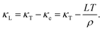
Fig. 8(a) displays the κT of various cooled InSb samples with respect to temperature. The κT is the combination of electronic thermal conductivity (κe) and lattice thermal conductivity (κT), which is represented using the following equation:55,56
 |
| | Fig. 8 (a)–(e) Total thermal conductivity (κT) (a), electronic thermal conductivity (κe) (b), lattice thermal conductivity (κL) (c), and temperature-dependent Lorentz number (L) (d) of InSb samples with cooling rates as a function of temperature and thermal conductivity comparison for various reported values (e). | |
The κT decreased as the cooling rate of the samples increased. The SC InSb has the κT of 7.29 W m−1 K−1 at 573 K, and it reduces to 6.60 W m−1 K−1 at the same temperature for the IWQ InSb. Fig. 8(b) shows the κe of the InSb samples at various temperatures. The κe was calculated using the following equation:
| |  | (5) |
The κe increased due to decrease in the ρ of the samples with the cooling rate. Fig. 8(c) shows the temperature-dependent Lorentz number (L) of the prepared InSb samples at different cooling rates. The magnitude of L was calculated using the measured S values and their relations, as shown in the following equation (eqn (6)):55,56
| |  | (6) |
The L was increased as a function of the cooling rate due to the decrease in ρ.
Fig. 8(d) illustrates the κL of the InSb samples as a function of temperature. The κL was extracted by subtracting the κe from κT, using the following equation:57
| |  | (7) |
The κL decreased as the cooling rates of the sample increased. The κL decreased with increasing temperature due to enhanced phonon–phonon Umklapp scattering, reducing the phonon mean free path at elevated temperatures. In addition, the EBSD images confirm a systematic reduction in grain size at the centres and edges from 910 µm and 905 µm in the SC InSb sample to 213 µm and 158 µm in the IWQ sample, respectively, leading to a significant increase in grain boundary density. These grain boundaries act as effective phonon scattering centers, further limiting thermal transport. The combined effect of intrinsic phonon–phonon scattering and extrinsic grain boundary scattering results in a pronounced suppression of κL, particularly in the fine-grain structured IWQ InSb samples. The grain boundary character distributions of the SC InSb, AQ InSb, and IWQ InSb samples are shown in Table S4 (a)–(c). SC InSb contains only low-angle Σ3 and Σ9 boundaries, resulting in weaker phonon scattering and higher lattice thermal conductivity (κl). In the AQ InSb sample, additional high-angle boundaries (Σ27a, Σ27b, and Σ19a) were present, which enhanced phonon scattering and reduced κL. IWQ InSb contains the highest fraction of higher angle boundaries (Σ27a, Σ27b, Σ35b, and Σ19b), leading to the strongest phonon scattering, which resulted in the lowest κL among all samples. Fig. 8(e) shows the thermal conductivity comparisons with the reported values of similar materials.46,48,49,53,58,59 The measured thermal conductivity of the samples is relatively lower than that of the reported values.
Furthermore, as evident from XRD analysis, the increased structural disorder promotes phonon scattering, leading to reduced κL. The broadening of peaks and lower wavenumber shifts in the Raman spectra (Fig. 4) further confirm the lattice distortion in the IWQ sample compared to the SC sample. As shown in EBSD images (Fig. 3(a1)–(c2)), the IWQ InSb sample has smaller-sized grains compared to the SC InSb sample. As a result, the IWQ InSb sample has a greater number of grain boundaries, as shown in Fig. 3(c1) and (c2), which are responsible for effective scattering of phonons, leading to decreased κL. A schematic of the phonon scattering mechanism is shown in Fig. 9.
 |
| | Fig. 9 Schematic of phonon scattering mechanisms for the SC InSb and IWQ InSb samples. | |
3.8 Figure of merit of InSb ingots with different cooling rates
Fig. 10(a) demonstrates the zT value of the prepared InSb samples with various cooling rates as a function of temperature. The zT was calculated using the PF and κT as a function of temperature. To obtain a high zT value, an extremely high PF and low κL are essential. Among all the samples, the IWQ InSb sample shows high PF and low κL. As a result, a higher zT value of 0.60 was achieved at 573 K for the IWQ InSb sample compared to the SC InSb sample (zT of 0.46 at 573 K). The zT values were compared with those of previous studies, as shown in Fig. 10(b).46,48,49,53,58,59 The obtained zT values are relatively higher than those of previously reported similar materials.
 |
| | Fig. 10
zT value of InSb samples (a) with cooling rate as a function of temperature and comparison chart for various reported studies (b). | |
4. Conclusion
The polycrystalline InSb samples were prepared using the melt quenching technique at different cooling rates. The structural and surface morphological investigation of the samples was extensively carried out using XRD and FESEM. The ρ slightly decreased with increasing cooling rates. The S of the prepared InSb samples was measured up to 573 K. A high PF of 6951 µW m−1 K−2 was achieved for the IWQ InSb sample at 573 K compared to the SC InSb sample (5935 µW m−1 K−2 at 573 K). κT is reduced for the IWQ InSb sample (6.60 W m−1 K−1) compared to SC InSb (7.29 W m−1 K−1) at 573 K due to modification in the grain structures and grain boundary densities, which enhanced the phonon scattering in the IWQ sample. As a result, a high zT value of 0.60 was achieved at 573 K for the IWQ InSb sample compared to the SC InSb sample (zT of 0.46 at 573 K). The experimental results demonstrate that grain structure modification through the melt quenching process is an effective approach for enhancing the TE performance of InSb.
Author contributions
M. Sivakumar: conceptualization, methodology, formal analysis, investigation, validation, data curation, writing – original draft. J. Prasath: formal analysis, investigation. S. Senthamizh Raja: investigation, formal analysis. R. Annie Victoria Rose: formal analysis, investigation. J. Mani: formal analysis, investigation. L. C. Chuang: formal analysis, investigation, validation. Sri Sai Samhitha Gadhavajhala: formal analysis, data curation. Bhuvanesh Srinivasan: investigation, formal analysis, writing – review & editing. R. Jayavel: resources, writing – review & editing. K. Fujiwara: formal analysis, investigation, writing – review & editing, validation. M. Arivanandhan: conceptualization, project administration, resources, writing – review & editing, supervision.
Conflicts of interest
There are no conflicts to declare.
Data availability
The data supporting the findings of this study are available within the article and its supplementary information (SI). Supplementary information is available. See DOI: https://doi.org/10.1039/d6ma00062b.
Additional raw data are available from the corresponding author upon reasonable request.
Acknowledgements
This work was supported by the DST-INSPIRE Fellowship with INSPIRE code IF200541 awarded to M. S. The author M. S. would like to acknowledge the support from the Department of Science and Technology (DST), New Delhi, Government of India, for the award of DST Inspire Fellowship (Reference No: DST/INSPIRE FELLOWSHIP/2020/IF200541). The work is financially supported by the GIMRT collaborative project (202308-RDKGE-0536, 202408-RDKGE-0534), Tohoku University, Sendai, Japan. S. S. S. G. thanks PMRF for the fellowship. B. S. thanks the Anusandhan National Research Foundation (ANRF/erstwhile SERB) for the funding (File Numbers SRG/2023/002282 and CRD/2024/000912) and IIT-Madras for the seed grant (NFSG).
References
- Y. Li, X. Wang, D. Luo, Y. Shi, Y. Ren and Y. Yan, e-Prime – Adv. Electr. Eng. Electron. Energy, 2023, 4, 100180 CrossRef.
- T. Hong, C. Guo, D. Wang, B. Qin, C. Chang, X. Gao and L. D. Zhao, Mater. Today Energy, 2022, 25, 100985 CrossRef CAS.
-
Z. G. Chen, G. Hana, L. Yanga, L. Cheng and J. Zou, 2012, preprint DOI:10.1016/j.pnsc.2012.11.011.
-
L. Wang, T. Chu, S. Yuan, P. Zou, W. Zhai, X. Zheng and M. Xia, 2025, preprint DOI:10.1016/j.enconman.2025.119621.
- A. P. Sobha and S. K. Narayanankutty, IEEE Trans. Nanotechnol., 2014, 13, 835–841 Search PubMed.
-
O. Caballero-Calero, J. R. Ares and M. Martín-González, 2021, preprint DOI:10.1002/adsu.202100095.
-
H. Mamur, Ö. F. Dilmaç, J. Begum and M. R. A. Bhuiyan, 2021, preprint DOI:10.1016/j.clema.2021.100030.
-
R. Singh, S. Dogra, S. Dixit, N. I. Vatin, R. Bhardwaj, A. K. Sundramoorthy, H. C. S. Perera, S. P. Patole, R. K. Mishra and S. Arya, 2024, preprint DOI:10.1016/j.hybadv.2024.100176.
- Y. Liu, G. Song, K. Tai, Z. Yu, Y. Ran, J. He and Y. Wu, Thin Solid Films, 2025, 809, 140585 CrossRef CAS.
-
L. Huang, Y. Zheng, L. Xing and B. Hou, 2023, preprint DOI:10.1016/j.tsep.2023.102064.
-
S. H. Zaferani, M. W. Sams, R. Ghomashchi and Z. G. Chen, 2021, preprint DOI:10.1016/j.nanoen.2021.106572.
- Z. Zhou, J. Yang, Q. Jiang, Y. Luo, D. Zhang, Y. Ren, X. He and J. Xin, J. Mater. Chem. A, 2016, 4, 13171–13175 RSC.
- A. Sampathu, M. Sivakumar, R. Chellakumar, D. Narendran, J. Kasthuri, S. Kumaran, M. Arivanandhan and M. Balakrishnan, Mater. Sci. Semicond. Process., 2025, 204, 110284 CrossRef.
- P. H. M. Böttger, K. Valset, S. Deledda and T. G. Finstad, J. Electron. Mater., 2010, 39, 1583–1588, DOI:10.1007/s11664-010-1269-2.
- R. Annie Victoria Rose, D. Sidharth, M. Sivakumar, J. Kasthuri, B. Srinivasan, R. Jayavel and M. Arivanandhan, ChemPhysChem, 2025, 26, e202500395 CrossRef PubMed.
- Y. Yu, C. Zhou, T. Ghosh, C. F. Schön, Y. Zhou, S. Wahl, M. Raghuwanshi, P. Kerres, C. Bellin, A. Shukla, O. Cojocaru-Mirédin and M. Wuttig, Adv. Mater., 2023, 35, 2300893 CrossRef CAS PubMed.
-
Q. Xiong, G. Han, G. Wang, X. Lu and X. Zhou, 2024, preprint DOI:10.1002/adfm.202411304.
- Q. Jian, Y. Gong, C. Chen, R. Sun, S. Zhao, T. Shen, Q. Zhang, Y. Geng, Y. Li, W. Dou, C. Liang, Y. Liu, D. Xiang, P. Ying and G. Tang, ACS Appl. Mater. Interfaces, 2025, 17, 15527–15534 Search PubMed.
- J. Chen, L. Wang, D. Ren, Y. Chu, Y. Wu, K. Meng, J. Miao, X. Xu and Y. Jiang, Synth. Met., 2018, 239, 13–21 CrossRef CAS.
- W. Li, Z. Yu, C. Liu, Y. Peng, B. Feng, J. Gao, G. Wu, X. Bai, J. Chen, X. Wang and L. Miao, J. Adv. Ceram., 2023, 12, 1511–1520 CrossRef CAS.
- L. L. Huang, J. Zhang, Z. M. Wang, X. G. Zhu, J. M. Li, C. Zhu, D. Li, C. J. Song, H. X. Xin and X. Y. Qin, Materialia, 2018, 3, 169–173 CrossRef CAS.
- L. Xie, H. Tong, G. Peng, H. Wu, W. Shi, K. Yu, J. Hu, L. Jiao, X. Dong, F. Guo, W. Cai, Y. Zhang, H. Wu, Z. Liu and J. Sui, Nat. Commun., 2025, 16, 7484 CrossRef CAS PubMed.
- V. C. S. Theja, V. Karthikeyan, D. S. Assi, H. Huang, C. H. Shek and V. A. L. Roy, Adv. Energy Sustainability Res., 2023, 4, 2300125 CrossRef CAS.
- V. P. Kannan, V. Lourdhusamy, I. Paulraj, C. J. Liu and M. Sridharan, ACS Appl. Mater. Interfaces, 2023, 15, 47058–47069, DOI:10.1021/acsami.3c10418.
- S. Perumal, S. Roychowdhury and K. Biswas, Inorg. Chem. Front., 2016, 3, 125–132 RSC.
- Q. Wang, Z. Li, L. Xu, T. Jiang, J. Wang, X. Qian and S. Wang, Mater. Today Phys., 2022, 27, 100818 CrossRef CAS.
- Q. Zhang, Z. Xiong, J. Jiang, W. Li, G. Xu, S. Bai, P. Cui and L. Chen, J. Mater. Chem., 2011, 21, 12398–12401 RSC.
- Y. Luo, J. Yang, Q. Jiang, W. Li, Y. Xiao, L. Fu, D. Zhang, Z. Zhou and Y. Cheng, Nano Energy, 2015, 18, 37–46 CrossRef CAS.
- C. Wang, D. Cong, G. Tang, X. Zhou and J. Li, Chem. Eng. J., 2024, 496, 154313 CrossRef CAS.
- Q. Q. Wang, K. F. Liu, Y. Y. Su, X. C. Liu, Q. Liu, S. Zhou, J. Liu and S. Q. Xia, Acta Mater., 2023, 255, 119028 CrossRef CAS.
- K. Zhang, Y. Huang, S. Liu, Q. Xiong, S. Zheng, B. Zhang, G. Wang, Y. Pan, G. Han, G. Wang, X. Lu, X. Chen and X. Zhou, Adv. Mater., 2025, 37, 2503496 CrossRef CAS PubMed.
- N. Grevtsov, E. Chubenko, V. Bondarenko, I. Gavrilin, A. Dronov, S. Gavrilov, D. Goroshko, O. Goroshko, G. Rymski and K. Yanushkevich, Mater. Res. Bull., 2025, 184, 113258 CrossRef CAS.
- T. Zhu, K. Swaminathan-Gopalan, K. Stephani and E. Ertekin, Phys. Rev. B, 2018, 97, 174201 CrossRef CAS.
- T. Palasyuk, C. Jastrzebski, A. Khachapuridze, E. Litwin-Staszewska, T. Suski, I. Grzegory and S. Porowski, Phys. Status Solidi RRL, 2024, 18, 2400093 Search PubMed.
- R. Abinaya, J. Archana, S. Harish, M. Navaneethan, C. Muthamizhchelvan, S. Ponnusamy, H. Udono, R. Sugahara, Y. Hayakawa and M. Shimomura, J. Colloid Interface Sci., 2021, 584, 295–309 Search PubMed.
- D. K. Meena, R. S. C. Bose, S. Vinoth, K. Annapurna and K. Ramesh, Appl. Phys. A, 2022, 128, 528 Search PubMed.
-
X. Tang, Z. Li, W. Liu, Q. Zhang and C. Uher, 2022, preprint DOI:10.1002/idm2.12009.
- J. D. Henderson, L. Pearson, H. Y. Nie and M. C. Biesinger, Surf. Interface Anal., 2025, 57, 81–97 Search PubMed.
- A. Vishwakarma, N. S. Chauhan, R. Bhardwaj, K. K. Johari, S. R. Dhakate, B. Gahtori and S. Bathula, J. Electron. Mater., 2021, 50, 364–374 CrossRef CAS.
- S. Perumal, M. Samanta, T. Ghosh, U. S. Shenoy, A. K. Bohra, S. Bhattacharya, A. Singh, U. V. Waghmare and K. Biswas, Joule, 2019, 3, 2565–2580 CrossRef CAS.
-
C. Liu, Z. Zhang, Y. Peng, F. Li, L. Miao, E. Nishibori, R. Chetty, X. Bai, R. Si, J. Gao, X. Wang, Y. Zhu, N. Wang, H. Wei and T. Mori, Charge transfer engineering to achieve extraordinary power generation in GeTe-based thermoelectric materials, 2023.
- V. Nirmal Kumar, Y. Hayakawa, H. Udono and Y. Inatomi, Intermetallics, 2019, 105, 21–28 CrossRef CAS.
- Y. Chen, X. L. Shi, D. Li, J. Zhu, M. Li, L. Zhang, Z. Zhang, Z. Feng, X. Ma, H. Zhong, S. Li and Z. G. Chen, Acta Mater., 2025, 286, 120736 CrossRef CAS.
- M. Jin, X. Bai, Z. Tang, S. Zhao, Y. Chen, L. Zhou, Y. Peng, X. Chen and X. Xu, Mater. Res. Bull., 2021, 142, 111411 CrossRef CAS.
- D. Besson, M. Treilleux, A. Hoareau and C. Esnouf, Philos. Mag. A, 2000, 80, 1139–1149 CAS.
- Y. Cheng, J. Yang, Q. Jiang, D. He, J. He, Y. Luo, D. Zhang, Z. Zhou, Y. Ren and J. Xin, J. Mater. Chem. A, 2017, 5, 5163–5170 RSC.
- K. Wang, P. Qin, Z. H. Ge and J. Feng, Mater. Lett., 2017, 209, 373–375 CrossRef CAS.
- S. Yamaguchi, T. Matsumoto, J. Yamazaki, N. Kaiwa and A. Yamamoto, Appl. Phys. Lett., 2005, 87, 1–3 CrossRef.
- S. Ghosh, S. M. Valiyaveettil, G. Shankar, T. Maity, K. H. Chen, K. Biswas, S. Suwas and R. C. Mallik, ACS Appl. Energy Mater., 2020, 3, 635–646 CrossRef CAS.
- W. Li, T. Xu, Z. Ma, Y. Cheng, J. Li, Q. Jiang, Y. Luo and J. Yang, Mater. Today Energy, 2022, 29, 101091 CrossRef CAS.
- M. Sivakumar, D. Sidharth, B. Srinivasan and M. Arivanandhan, J. Alloys Compd., 2024, 1009, 176908 CrossRef CAS.
- L. L. Huang, J. Zhang, Z. M. Wang, X. G. Zhu, J. M. Li, C. Zhu, D. Li, C. J. Song, H. X. Xin and X. Y. Qin, Materialia, 2018, 3, 169–173 CrossRef CAS.
- J. Palraj, M. Moorthy, S. Katlakunta and S. Perumal, Ceram. Int., 2022, 48, 29284–29290 CrossRef CAS.
- Z. Lu, B. Huang, G. Li, X. Zhang, Q. An, B. Duan, P. Zhai, Q. Zhang and W. A. Goddard, npj Comput. Mater., 2021, 7, 111 Search PubMed.
- R. Annie Victoria Rose, D. Sidharth, M. Arivanandhan and R. Jayavel, New J. Chem., 2024, 48, 11506–11517 Search PubMed.
- D. Sidharth, I. Paulraj, V. Lourdhusamy, M. Arivanandhan and C. J. Liu, J. Eur. Ceram. Soc., 2024, 44, 954–960 Search PubMed.
- D. Sidharth, B. Srinivasan, A. S. A. Nedunchezhian, P. Thirukumaran, M. Arivanandhan and R. Jayavel, J. Phys. Chem. Solids, 2022, 160, 110303 CrossRef CAS.
- D. Zhang, H. Wu, Z. Zhou, S. Zheng, B. Zhang, Y. Zhou, X. Lu and X. Zhou, Mater. Today Phys., 2023, 32, 101020 CrossRef CAS.
- Z. Du, X. Chen, J. Zhu and J. Cui, Curr. Appl. Phys., 2018, 18, 893–897 CrossRef.
|
| This journal is © The Royal Society of Chemistry 2026 |
Click here to see how this site uses Cookies. View our privacy policy here. 
 Open Access Article
 This Open Access Article is licensed under a Creative Commons Attribution-Non Commercial 3.0 Unported Licence
 a,
J.
Prasath
a,
S. Senthamizh
Raja
a,
R. Annie Victoria
Rose
a,
J.
Mani
b,
L. C.
Chuang
c,
Sri Sai Samhitha
Gadhavajhala
d,
Bhuvanesh
Srinivasan
a,
J.
Prasath
a,
S. Senthamizh
Raja
a,
R. Annie Victoria
Rose
a,
J.
Mani
b,
L. C.
Chuang
c,
Sri Sai Samhitha
Gadhavajhala
d,
Bhuvanesh
Srinivasan

 and reducing the thermal conductivity.13 The PF can be enhanced by hetero valence substitution,14,15 doping,12,16,17 compositing,18–20 and nano-inclusions.21–23 Thermal conductivity can be suppressed through nano-structuring24–26 of the material, defect engineering,27–29 point defect scattering,27,28 grain boundary engineering,30,31 phonon engineering,24,32–35 and melt quenching.32,36 Good thermoelectric materials behave like phonon glass–electron crystal (PGEC).33 However, in general, the thermal and electrical conductivities are coupled. Therefore, it is quite difficult to enhance the performance of TE energy harvesting materials by decoupling their electrical and thermal conductivities. Semiconductors are suitable materials for improving the zT value of the material37 because semiconductors have optimum carrier concentrations and tunable bandgaps as well as low thermal conductivity.38 A lot of semiconductor materials exhibit high TE performance. Bi2Te336,37 and Si1−xGex39 are familiar semiconductor materials for low- and high-temperature TE applications, respectively. However, an appropriate functional material for mid-temperature TE applications is still lacking, despite the high performance of a few materials such as SnSe and GeTe.40,41


