DOI:
10.1039/D6MA00009F
(Paper)
Mater. Adv., 2026,
7, 3407-3438
Harnessing the untapped potential of a lanthanide-based perovskite (RbYbCl3) absorber: from material properties to device implementation
Received
4th January 2026
, Accepted 11th February 2026
First published on 12th February 2026
Abstract
The increasing demand for clean and sustainable energy has led to intensified research into lead-free perovskite materials as potential alternatives for next-generation photovoltaic devices. This study investigates the highly promising lanthanide-based perovskite RbYbCl3 as a stable and efficient absorber using a multiscale approach that combines first-principles analysis with device-level simulations. Structural optimization through Birch–Murnaghan equation of state (EOS) fitting confirmed the thermodynamic stability of the cubic perovskite phase (Pm![[3 with combining macron]](https://www.rsc.org/images/entities/char_0033_0304.gif) m). Additionally, electronic structure calculations revealed a direct band gap that falls within the optimal range for solar energy harvesting. The direct band gaps calculated using both the PBEsol and TB-mBJ methods were found to be 0.343 eV and 1.713 eV, respectively. Optical analysis indicated a strong absorption coefficient (∼105 cm−1), low reflectivity, and minimal energy loss across the visible and ultraviolet spectrum, highlighting the material's suitability for photovoltaic applications. To translate these intrinsic properties into practical applications, SCAPS-1D simulations were conducted using tailored transport layers. Among 64 combinations, we tested devices with IGZO, SnS2, WO3, and ZnO as electron transport layers (ETLs) and Cu2O as the hole transport layer (HTL) in the configuration FTO/ETL/RbYbCl3/Cu2O/Pt. The highest achieved power conversion efficiency was 25.06%, with an open-circuit voltage of 1.328 V, a short-circuit current of 22.85 mA cm−2, and a fill factor of 89.36% at an absorber thickness of ≥1.0 µm, which matches almost 95% of the Shockley–Queisser limit for solar cells. This study demonstrates a strong correlation between material-level properties and device-level outcomes, establishing RbYbCl3 as a promising lanthanide-based, lead-free perovskite absorber. The findings not only expand the scope of rare-earth halide perovskites in photovoltaics but also pave the way for their future integration into scalable and stable solar energy technologies.
m). Additionally, electronic structure calculations revealed a direct band gap that falls within the optimal range for solar energy harvesting. The direct band gaps calculated using both the PBEsol and TB-mBJ methods were found to be 0.343 eV and 1.713 eV, respectively. Optical analysis indicated a strong absorption coefficient (∼105 cm−1), low reflectivity, and minimal energy loss across the visible and ultraviolet spectrum, highlighting the material's suitability for photovoltaic applications. To translate these intrinsic properties into practical applications, SCAPS-1D simulations were conducted using tailored transport layers. Among 64 combinations, we tested devices with IGZO, SnS2, WO3, and ZnO as electron transport layers (ETLs) and Cu2O as the hole transport layer (HTL) in the configuration FTO/ETL/RbYbCl3/Cu2O/Pt. The highest achieved power conversion efficiency was 25.06%, with an open-circuit voltage of 1.328 V, a short-circuit current of 22.85 mA cm−2, and a fill factor of 89.36% at an absorber thickness of ≥1.0 µm, which matches almost 95% of the Shockley–Queisser limit for solar cells. This study demonstrates a strong correlation between material-level properties and device-level outcomes, establishing RbYbCl3 as a promising lanthanide-based, lead-free perovskite absorber. The findings not only expand the scope of rare-earth halide perovskites in photovoltaics but also pave the way for their future integration into scalable and stable solar energy technologies.
1. Introduction
The growing global population and rapid industrialization continue to drive increasing energy demand, which remains heavily dependent on fossil fuels such as coal, oil, and natural gas.1 This dependence accelerates resource depletion and contributes to severe environmental and societal challenges.2–5 Consequently, the transition toward sustainable and environmentally friendly energy sources has become imperative. Among renewable technologies, solar energy has emerged as one of the most promising solutions due to its abundance, scalability, and minimal environmental impact.6 In this context, perovskite solar cells (PSCs) have gained remarkable attention owing to their excellent optoelectronic properties, tunable bandgaps, low fabrication cost, and rapidly improving power conversion efficiency (PCE).7,8
Thin-film PSCs, in particular, have attracted significant attention due to their rapid rise in efficiency and cost-effective fabrication and best environmental impact. Organic-based perovskites such as CH3NH3PbI3 are excellent light harvesters and have played a pivotal role in driving efficiency improvements.9,10 Since their emergence in 2009 as efficient photon absorbers,11 hybrid halide PSCs have achieved efficiencies surpassing 10% within a few years,12 with record values reaching 22.7% and further advancing to 47.1% using multi-junction concentrator solar cells in the United States.13 Despite this remarkable progress, the instability of organic-based perovskites under humidity, temperature, and UV exposure, together with the toxicity of lead (Pb), has hindered their path to commercialization.14,15 These challenges have motivated intensive research into lead-free alternatives, with various classes such as Sn- and Ge-based perovskites, Bi- and Sb-based compounds, and rare-earth halides being explored.16 For instance, Azmat et al. reported that CsTmCl3 exhibits direct bandgaps of 1.18 eV (without SOC) and 0.99 eV (with SOC), highlighting its suitability for optoelectronic applications.17 While Pb-based PSCs still hold the record for high efficiencies (up to 20.1%),18 lead-free inorganic variants like CsSnI3, CsSnBr3, and CsGeBr3 have shown lower efficiencies due to oxidation and instability issues.19 Similarly, Brik et al.20 found that CsABr3 (A = Sn, Ge, Ca) in cubic form exhibited high susceptibility to substitution, with CsGeBr3 presenting a bandgap smaller than the experimental 2.32 eV, while Schwarz et al.21 demonstrated pressure-dependent absorption in CsGeCl3/Br3, underscoring the tunability of halide perovskites. Altogether, these studies highlight both the immense promise and the persistent challenges of lead-free perovskites, and they establish a strong rationale for further exploration of novel systems, particularly rare-earth halide perovskites, as a viable pathway toward stable, efficient, and environmentally friendly solar energy technologies.
In recent years, rare-earth halide perovskites with the general formula A–Ln–X3 have emerged as promising candidates due to their enhanced chemical stability, non-toxicity, and tunable optoelectronic properties.22,23 The incorporation of lanthanide ions introduces localized f–f transitions and enhances structural stability, making these materials suitable for optoelectronic, photovoltaic, and thermoelectric applications.24–27 Among them, Tm3+ based halide perovskites, notably CsTmCl3 and RbTmCl3, have gained recent attention due to their favorable direct bandgaps (1.4–1.6 eV), strong optical absorption, and robustness under ambient conditions.17,28 However, the radioactive nature of Tm limits its practical applicability in solar cell technologies, necessitating alternative lanthanide candidates. In this circumstance, ytterbium-based halide perovskites have recently attracted increasing interest due to the unique 4f13 electronic configuration of Yb3+ ions. The sharp f–f transitions of Yb3+ enable strong optical absorption extending from the visible to the near-infrared region, making these materials suitable for photovoltaic, infrared detection, and photonic applications.29
In particular, RbYbCl3 crystallizes in a cubic perovskite-like Pmm structure composed of corner-sharing [YbCl6]3− octahedra with Rb+ ions occupying the A-sites. This structural configuration promotes strong hybridization between Yb-4f and Cl-3p states, governing band dispersion and bandgap formation. First-principles DFT studies have reported RbYbCl3 as a direct-bandgap semiconductor with a gap of approximately 1.42 eV using the TB-mBJ potential, along with strong visible-NIR absorption and favorable carrier transport properties.29,30 Moreover, halogen substitution (e.g., Cl → Br → I) in ALnX3 systems has been demonstrated to effectively tune the bandgap, refractive index, and absorption edge, providing a viable route for chemical optimization. For example, CsYbI3 and RbYbI3, investigated through WIEN2k-based DFT calculations, exhibited direct bandgaps of 1.22 eV and 1.12 eV, respectively, with strong polarization and enhanced absorption between 1.5 and 3.1 eV, emphasizing their potential in solar energy conversion.31 Despite these encouraging findings, chloride-based ytterbium perovskites, particularly RbYbCl3, remain largely unexplored for photovoltaic applications. Their chemical robustness, favorable bandgap, and lead-free nature highlight their potential as next-generation absorber materials. While Pb- and Ge-based perovskites such as CsPbX3 and AGeX3 have achieved efficiencies exceeding 20%,32 ytterbium-based systems are expected to offer superior stability and environmentally benign alternatives with competitive optoelectronic performance.
In this study, we explore the untapped potential of RbYbCl3 by analyzing its structural, electronic, and optical properties using DFT calculations carried out in WIEN2k. After evaluating these material properties, we implement RbYbCl3 as an absorber layer in a device structure of FTO/ETL/RbYbCl3/HTL/Pt, exploring several electron transport layers (ETLs), and select the highest performing ETLs IGZO, SnS2, WO3, and ZnO, while adopting Cu2O as the hole transport layer (HTL) for our device configurations. Efficient charge transport layers are critical for achieving high-performing PSCs. IGZO offers high electron mobility and optical transparency, ensuring efficient charge extraction.33 SnS2 provides favorable band alignment, enhancing photocurrent and reproducibility.34,35 WO3, with excellent electron selectivity, suppresses recombination losses.36 ZnO, widely used for its high transparency, mobility, and cost-effectiveness, remains a benchmark ETL.37 For a HTL, Cu2O is an earth-abundant, stable, and highly efficient alternative to conventional organic transport layers, offering wide bandgap, high hole mobility, and excellent environmental stability.38–40 Thus, our work aims to highlight the potential of RbYbCl3 as a lead-free absorber for PSCs and related optoelectronic applications. Through a multiscale analysis, we investigate both the material properties (via DFT) and the device-level performance (via SCAPS-1D simulations). Performance parameters such as current density–voltage (J–V) characteristics, external quantum efficiency (EQE), series/shunt resistance effects, absorber thickness, defect density, and temperature dependence are systematically analyzed. The outcomes of this study provide valuable insights into the suitability of RbYbCl3 for next-generation clean energy technologies and contribute toward advancing sustainable, lead-free perovskite photovoltaics.
2. Methodology
2.1. Theoretical framework for DFT analysis
The optoelectronic and optical properties of RbYbCl3 were calculated within the framework of density functional theory (DFT) using the WIEN2k simulation package,41,42 which employs the full-potential linearized augmented plane wave (FP-LAPW) method. The computational protocol involved three major stages: (i) structural optimization, (ii) electronic structure evaluation, and (iii) derivation of optical constants. For structural optimization, the generalized gradient approximation (GGA) in the form of the Perdew–Burke–Ernzerhof revised for solids (PBEsol) functional42 was used. The muffin-tin radii (RMT) were set to 2.50 a.u. for Rb, 2.20 a.u. for Yb, and 2.00 a.u. for Cl, with the cutoff parameter RMTKmax = 7.0. Brillouin-zone integrations were carried out using a 10 × 10 × 10 Monkhorst–Pack grid (1000 k-points in the full zone). Convergence was assumed when the total energy difference between iterations was below 10−5 Ry and the charge difference was less than 10−3. The total energy as a function of unit-cell volume was fitted to the third-order Birch–Murnaghan equation of state (EOS), yielding the optimized lattice constant, equilibrium volume, bulk modulus, and pressure derivative. The electronic band structure was traced along the high-symmetry k-path R–Γ–X–M–Γ, while the total and projected density of states (TDOS and PDOS) were obtained using the tetrahedral integration method. To overcome the well-known bandgap underestimation of GGA, the Tran–Blaha modified Becke–Johnson (TB-mBJ) potential43,44 was employed, leading to more accurate predictions of the electronic gap and band dispersion.
The optical properties were derived from the frequency-dependent dielectric function, ε(ω) = ε1(ω) + iε2(ω), within the independent-particle approximation. The real and imaginary components of the dielectric function were computed, from which the secondary optical constants, including the absorption coefficient α(ω), refractive index n(ω), reflectivity R(ω), optical conductivity σ(ω), and energy-loss function L(ω), were obtained using the Kramers–Kronig relations. The governing relations are summarized below:45,46
| |  | (1) |
| | 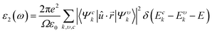 | (2) |
| | 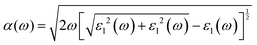 | (3) |
| | 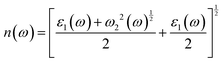 | (4) |
| | 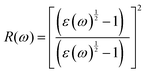 | (5) |
| |  | (6) |
where
α(
ω) is the absorption coefficient,
n(
ω) is the refractive index,
R(
ω) is the reflectivity,
L(
ω) is the energy loss function, and
ε1(
ω) and
ε2(
ω) are the real and imaginary parts of the dielectric function, respectively. These relations provide the theoretical basis for analyzing the interaction of photons with the RbYbCl
3 crystal. It is noted that certain DFT-derived physical parameters, such as the dielectric constant and refractive index, were not explicitly calculated in this study. The focus here is on the electronic structure, bandgap, and photovoltaic performance of RbYbCl
3, which are sufficient to assess its potential as a Pb-free perovskite absorber. Previous studies (Mahmood
et al. (2021)
29) report slightly different values for these parameters, which is common in DFT calculations due to variations in (i) exchange–correlation functionals, (ii) pseudopotentials, (iii)
k-point sampling and convergence criteria, and (iv) structural optimization methods. For instance, GGA-based functionals typically underestimate the bandgap and may influence derived optical constants, whereas hybrid functionals generally yield higher values. Despite these differences, the overall trends indicate that RbYbCl
3 possesses favorable optical and dielectric properties for photovoltaic applications, supporting its suitability as a Pb-free absorber.
2.2. Device simulation methodology of solar cells
Following the electronic and optical property evaluation, the selected materials will be integrated into device-level simulations using SCAPS-1D (solar cell capacitance simulator), a numerical simulation tool developed by the University of Ghent for modeling thin-film heterojunction solar cells. SCAPS solves the coupled drift-diffusion equations under steady-state conditions for electrons and holes, along with Poisson's equation to evaluate the internal electrostatic potential.47,48 The Poisson equation is given by:49| | 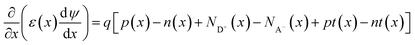 | (7) |
where ψ(x) is the electrostatic potential, q is the elementary charge, ε is the permittivity of the material, p(x) and n(x) are the hole and electron densities, and ND+ and NA− are the ionized donor and acceptor concentrations. The current continuity equations for electrons and holes are:| |  | (8) |
| |  | (9) |
Under this situation, Jn and Jp correspondingly reflect the current density of holes as well as electrons. Rn and Rp show the relative recombination rates; Gn and Gp show the hole in addition to the electron generation rates.
The charge carrier drift-diffusion equations used to calculate the hole and electron current density values in solar cell structures are given by eqn (10) and (11).
The diffusion coefficients of holes and electrons are represented by Dn and Dp, respectively, and their mobility by μn and μp. According to Einstein's relation, the lifetime of the carrier and its mobility significantly influence the diffusion coefficient. The absorption constant of the films was also determined using the new Eg-sqrt model, which is a better alternative to the traditional sqrt (hν − Eg) model. To express the correlation, eqn (12) employs the “Tauc laws.”
| |  | (12) |
In this case, hν stands for the energy of photons, Eg for the band gap and β for the absorption coefficient. Eqn (13) and (14) show how the model's variables α0 and β0 relate to the traditional model variables A and B:
| |  | (13) |
| |  | (14) |
SCAPS-1D was employed to perform steady-state simulations of the designed photovoltaic devices. The workflow, illustrated in Fig. 1, begins with defining the device structure, where RbYbCl3 was selected as the active perovskite absorber in combination with different ETLs. Device inputs included band gap, electron affinity, dielectric constant, carrier mobilities, and defect densities for each layer. Operational conditions such as illumination (AM 1.5G, 100 mW cm−2), temperature (300 K), and the bias sweep range were also specified. From these inputs, the model generated key device characteristics, including current–voltage curves, capacitance response, Mott–Schottky behavior, and external quantum efficiency (EQE), enabling a comprehensive evaluation of cell performance.
 |
| | Fig. 1 Operational procedure of SCAPS-1D. | |
Tables 1 and 2 present the essential physical and electronic properties of the solar cell components, including FTO (front contact), ETLs, absorber RbYbCl3 and HTLs. Key parameters such as bandgap, dielectric constant, electron affinity, and carrier mobility play a significant role in SCAPS-1D simulations, influencing the open-circuit voltage (VOC) and power conversion efficiency (PCE). Interface defect layers were also incorporated, with Table 2 detailing defect densities and capture cross-sections, which are critical for understanding recombination effects at the interfaces. The simulations employed the parameters listed in Table 1, while the absorption coefficient was calculated within SCAPS-1D using these inputs. Various ETL and HTL combinations were tested to optimize the absorber layers, and the highest efficiencies were identified by evaluating VOC, short-circuit current density (JSC), and fill factor (FF). Additionally, the study examined the impact of varying absorber, ETL, and HTL thicknesses and interface defect properties on the overall performance of the solar cells.
Table 1 Input parameters for the layers of solar cells
| Parameters |
FTO33 |
ETLs |
HTL |
Absorber |
| IGZO50 |
SnS251 |
WO352 |
ZnO52 |
Cu2O50 |
RbYbCl3 |
| Thickness (nm) |
500 |
50 |
80 |
50 |
50 |
50 |
1000 |
| Bandgap, Eg (eV) |
3.5 |
3.05 |
2.24 |
2 |
3.35 |
2.2 |
1.713 |
| Electron affinity, Ea (eV) |
4 |
4.16 |
4.24 |
3.8 |
4 |
3.4 |
4 |
| Dielectric permittivity (relative), Er |
9 |
10 |
10 |
4.8 |
9 |
7.5 |
3.957 |
| CB effective density of states, NC (cm−3) |
2.2 × 10¹⁸ |
5 × 10¹⁸ |
2.2 × 10¹⁸ |
2.2 × 10²¹ |
3.7 × 10¹⁸ |
2.0 × 10¹⁹ |
4.591 × 10¹⁶ |
| VB effective density of states NV (cm−3) |
1.8 × 10¹⁹ |
5 × 10¹⁸ |
1.8 × 10¹⁹ |
2.2 × 10²¹ |
1.8 × 10¹⁹ |
1.0 × 10¹⁹ |
1.137 × 10¹⁹ |
| Electron mobility, µn (cm2 V−1 s−1) |
20 |
15 |
50 |
30 |
100 |
200 |
118.5 |
| Hole mobility, µh (cm2 V−1 s−1) |
10 |
0.1 |
50 |
30 |
25 |
8600 |
3.005 |
| Shallow uniform donor density, ND (cm−3) |
1 × 10¹⁸ |
1 × 10¹⁷ |
1 × 10¹⁶ |
6.35 × 10¹⁷ |
1 × 10¹⁸ |
0 |
0 |
| Shallow uniform acceptor density, NA (cm−3) |
0 |
0 |
1 × 10⁶ |
0 |
0 |
1 × 10¹⁸ |
1 × 10¹⁵ |
| Defect density, Nt (cm−3) |
1 × 10¹⁵ |
1 × 10¹⁵ |
1 × 10¹⁵ |
1 × 10¹⁵ |
1 × 10¹⁵ |
1 × 10¹⁵ |
1 × 10¹⁵ |
Table 2 Interface parameters used in designed solar cells51
| Interface |
ETL/absorber |
Absorber/HTL |
| Defect type |
Neutral |
Neutral |
| Electron capture cross-section (cm2) |
1 × 10⁻¹⁷ |
1 × 10⁻¹⁸ |
| Hole capture cross-section (cm2) |
1 × 10⁻¹⁸ |
1 × 10⁻¹⁹ |
| Energy distribution |
Single |
Single |
| Defect reference energy level, Et |
Above highest EV |
Above highest EV |
| Characteristic energy (eV) |
0.60 |
0.05 |
| Defect density (cm−3) |
1 × 10¹⁰ |
1 × 10¹⁰ |
2.3. Device structure and band alignment
The overall device configuration and corresponding band alignment are presented in Fig. 2a and b, respectively. As shown in Fig. 2a, the proposed RbYbCl3-based solar cell adopts the structure FTO/ETL/RbYbCl3/Cu2O/Pt, where FTO serves as the transparent front contact, RbYbCl3 functions as the light-absorbing layer, ETLs ensure selective electron extraction, Cu2O facilitates hole transport, and Pt acts as the hole-collecting back electrode. Fig. 2b illustrates the equilibrium band alignment of this architecture, highlighting the conduction band minimum (CBM) and valence band maximum (VBM) positions across the device stack. Four optimal ETLs, IGZO, SnS2, WO3, and ZnO, were analyzed to evaluate interfacial charge transport. ZnO and IGZO form favorable conduction-band offsets with RbYbCl3, enabling efficient electron injection while suppressing recombination. SnS2, although promising as a non-toxic ETL, exhibits a slightly deeper CBM that may introduce resistance to electron transport, whereas WO3 provides only moderate alignment, with possible interfacial mismatch. Overall, Cu2O exhibits excellent VBM alignment with RbYbCl3, ensuring effective hole extraction toward the Pt electrode. The device was designed in a conventional n–i–p configuration, where the ETL/RbYbCl3/HTL stack enables efficient charge separation and collection through a built-in electric field. This architecture is widely adopted in SCAPS-1D simulations as a benchmark structure to evaluate the photovoltaic feasibility of emerging absorber materials.53–58
 |
| | Fig. 2 (a) Schematic illustration of the proposed device structure FTO/ETL/RbYbCl3/HTL (Cu2O)/Pt. (b) Equilibrium energy band alignment diagrams of RbYbCl3-based solar cells with different ETLs and HTLs. | |
2.4. Synergy between DFT and SCAPS-1D approaches
Density functional theory (DFT) and SCAPS-1D complement each other by linking fundamental material properties to device-level performance. DFT calculations provide intrinsic electronic and optical parameters of the absorber and transport layers, such as band gap, effective masses, dielectric constant, and band edge positions. These parameters define the quality of charge transport, recombination dynamics, and band alignment at interfaces. SCAPS-1D incorporates these DFT-derived parameters as input to simulate the photovoltaic behavior of the complete device stack. For instance, the conduction band minimum (CBM) and valence band maximum (VBM) obtained from DFT determine the alignment of the absorber with the ETL and HTL, while the calculated dielectric constant and defect states influence carrier recombination and electrostatics. Thus, DFT provides the fundamental material descriptors, and SCAPS-1D translates them into measurable device characteristics such as VOC, JSC, fill factor (FF), and power conversion efficiency (PCE). This combined framework ensures that device simulations are not limited to empirical parameters but are instead grounded in first-principles insights, thereby enabling more accurate predictions of performance and guiding the optimization of novel perovskite-based solar cells.
3. Results and discussion
3.1. Structural properties and stability
The equilibrium structural parameters of RbYbCl3 were determined through total-energy minimization using the Birch–Murnaghan equation of state (EOS). The optimized cubic perovskite structure adopts the space group Pmm (no. 221), with Rb occupying the A-site (0, 0, 0), Yb at the B-site (0.5, 0.5, 0.5), and Cl at the X-site (0.5, 0.5, 0). The structural configuration is depicted in Fig. 3, where corner-sharing YbCl6 octahedra form a stable cubic framework, while Rb atoms occupy the cuboctahedra voids. The optimized lattice constant was calculated as 5.448 Å, with an equilibrium cell volume of 1091.23 bohr3. The calculated bulk modulus (B0 = 18.28 GPa) and pressure derivative (B′ = 8.89) indicate the mechanically soft nature of the halide perovskite lattice, in line with other inorganic halide perovskites.58–60 Such softness contributes to low lattice thermal conductivity, which is advantageous for thermoelectric performance. In addition, the energy–volume relationship of the examined compounds is shown in Fig. 4.
 |
| | Fig. 3 Crystal structure of RbYbCl3. | |
 |
| | Fig. 4 Variation of total energy as a function of unit cell volume for the RbYbCl3 perovskite. | |
To further assess the geometric stability of the cubic phase, the Goldschmidt tolerance factor (τg) was computed using Shannon's ionic radii.61,62 The tolerance factor (τg) and octahedral factor (μ) are critical parameters for evaluating the structural stability of double perovskite materials. These factors are determined using eqn (15) and (16).62–64
| |  | (15) |
| |  | (16) |
In eqn (15), rRb, rCl and rYb represent the ionic radii of Rb, Yb and Cl, respectively. A compound is considered to possess cubic stability if the tolerance factor (τg) falls within the range of 0.813 to 1.107 and the octahedral factor (μ) is between 0.41 and 0.89.65,66Table 3 shows that all the compounds analyzed meet these criteria, confirming their cubic stability. The tolerance factor was found to be tg = 0.93, while the octahedral factor was μ = 0.48. These values fall within the accepted range for stable perovskites, confirming that RbYbCl3 is structurally stable with minor octahedral distortions.
Table 3 Optimized structural parameters and stability factors of RbYbCl3
| Parameter |
Value |
| Lattice constant, a (Å) |
5.448 |
| Equilibrium volume, V0 (bohr3) |
1091.23 |
| Bulk modulus, B0 (GPa) |
18.28 |
| Pressure derivative, B′ |
8.89 |
| Equilibrium energy, E0 (Ry) |
−36![[thin space (1/6-em)]](https://www.rsc.org/images/entities/char_2009.gif) 884.5759 884.5759 |
| Tolerance factor, tg |
0.93 |
3.2. Electronic properties
3.2.1. Band structure.
To comprehensively evaluate a material's optoelectronic and photovoltaic performance, it is crucial to investigate its electronic properties, with particular emphasis on the energy band gap and the distribution of electronic states, including both total and element-specific densities of states. These characteristics are fundamental in determining the material's light absorption, electrical conductivity, and interaction with photons. The electronic band structures computed using PBEsol and PBEsol+TB-mBJ are presented in Fig. 5a and b, respectively energy states are plotted on the vertical axis, while the horizontal axis displays the wave vector (K) along important high-symmetry points of the bulk Brillouin zone. The band structure is analyzed along these high-symmetry points (W–L–Γ–X–W–K) in the Brillouin zone (BZ). A red dashed line at zero energy indicates the Fermi level, separating the valence band (VB) from the conduction band (CB). The energy range for the plotted band structure extends from −10 to +10 eV. Both functionals reveal that RbYbCl3 is a direct bandgap semiconductor with the VBM and CBM located at the Γ-point. However, there is a significant difference in the estimated bandgap values.
 |
| | Fig. 5 Electronic band structure of RbYbCl3 using (a) PBEsol and (b) PBEsol + TmBj. | |
The PBEsol functional predicts a very narrow direct gap of 0.343 eV, which reflects the well-known underestimation of band gaps in conventional GGA-based approximations. The flatness of the bands near the Fermi level, particularly around Γ, highlights the localized character of Yb-4f states, in line with earlier observations for rare-earth halide perovskites.67 When the TB-mBJ potential is applied, the bandgap increases substantially to 1.713 eV, bringing it closer to realistic values for semiconductors. Such a correction is consistent with the role of TB-mBJ in improving bandgap predictions by accounting for exchange–correlation effects more accurately.68 The direct gap at Γ ensures that electronic transitions do not require phonon assistance, enhancing optical absorption efficiency. Moreover, the TB-mBJ band structure shows greater conduction band dispersion compared to PBEsol, suggesting lower effective masses and higher carrier mobilities, which are favorable for optoelectronic applications such as photovoltaics and photodetectors.
3.2.2. Effect of spin–orbit coupling (SOC).
To further explore the relativistic effects induced by the heavy Yb atom, spin–orbit coupling (SOC) was incorporated in an additional TB-mBJ calculation. The inclusion of SOC introduces a pronounced interaction between the spin and orbital angular momenta of Yb's 4f and 5d electrons, which substantially modifies the electronic structure near the Fermi level. As a result, the bandgap decreases from 1.713 eV (without SOC) to approximately 1.094 eV (with SOC), Fig. S1. This reduction originates from the splitting of degenerate Yb-4f states and partial lowering of the conduction band minimum, leading to stronger hybridization between Yb-5d and Cl-3p orbitals. Such SOC-induced bandgap narrowing is a well-known phenomenon in rare-earth halide perovskites, where the heavy atomic mass of the B-site cation enhances relativistic corrections. Although SOC significantly affects the quantitative bandgap, it does not alter the direct-gap nature or the dispersion characteristics of the conduction and valence bands. The material therefore preserves its fundamental semiconducting behavior, ensuring efficient direct optical transitions (Table 4).
Table 4 Calculated bandgaps of RbYbCl3
| Functional |
Bandgap (eV) |
Gap type |
| PBEsol |
0.343 |
Direct |
| PBEsol+TB-mBJ |
1.713 |
Direct |
| PBEsol+TB-mBJ (with SOC) |
1.094 |
Direct |
3.2.3. Effective mass and transport properties.
The transport characteristics of RbYbCl3 were further analyzed in terms of its electronic parameters, which play a decisive role in optoelectronic and photovoltaic device performance. The relative dielectric permittivity (εr) was calculated as 3.957, indicating moderate dielectric screening that facilitates exciton binding, a common feature in halide perovskites. The effective density of states in the conduction (NC) and valence (NV) bands was obtained using the following expressions (eqn (17) and (18)).69| |  | (17) |
| |  | (18) |
where  and
and  are the effective masses of electrons and holes, KB is the Boltzmann constant, T is the temperature (300 K), and h is Planck's constant. The resulting values, NC = 4.591 × 1016 cm−3 and NV = 1.137 × 1019 cm−3, confirm the asymmetric contribution of carriers, with the valence band providing a substantially higher density of states than the conduction band. These parameters, evaluated at 300 K using the calculated electron and hole effective masses, offer important information on the density of available charge carriers and further confirm the semiconducting characteristics of the material. The larger value of NV relative to NC suggests a dominance of hole-related states, indicating a p-type transport behavior.69,70 The carrier mobility (μ) was estimated using the relaxation time approximation, expressed as eqn (19).72
| |  | (19) |
where e is the electronic charge and τ is the carrier relaxation time, set to 10−14 s for halide perovskites. The calculated electron mobility was μn = 118.5 cm2 V−1, while the hole mobility was much lower, μh = 3.005 cm2 V−1. This imbalance highlights the significantly lighter transport of electrons relative to holes, consistent with the conduction-band dispersion revealed by the band structure.
3.2.4. Density of states (DOS analysis).
The density of states (DOS) provides a quantitative description of the number of available electronic states at each energy level. The total DOS (TDOS) represents the overall distribution of electronic states across all atoms in the unit cell, while the projected DOS (PDOS) resolves these states into atomic and orbital contributions, allowing identification of the dominant orbitals near the band edges. The calculated TDOS and PDOS of RbYbCl3 are shown in Fig. 6a–d. The valence band region extending from −6 eV to the Fermi level is mainly dominated by Cl-3p states, which strongly hybridize with Yb-4f orbitals near the valence band maximum (VBM). This p–f interaction plays a decisive role in shaping the top of the valence band and is responsible for the covalent bonding character between Yb and Cl atoms. The conduction band minimum (CBM), on the other hand, is primarily formed by Yb-4f states, which appear as sharp, localized peaks just above the Fermi level, reflecting their strongly localized nature. In addition, contributions from Yb-5d orbitals are also evident at higher energies in the conduction band, leading to broader dispersion in this region and supporting enhanced electronic mobility. The Rb states, including Rb-s, Rb-p, and Rb-d, contribute negligibly around the Fermi level, confirming that Rb acts primarily as a structural stabilizer within the perovskite framework rather than participating directly in electronic transitions. The dominance of Cl-p states at the VBM and Yb-f states at the CBM confirms the direct bandgap character of RbYbCl3, consistent with the band structure results, where a TB-mBJ corrected bandgap of 1.713 eV was obtained. Such an electronic arrangement, with halogen-derived valence bands and rare-earth-derived conduction bands, has also been reported for similar Yb-based halide perovskites,25,32,58 suggesting that RbYbCl3 shares the same favorable features for optoelectronic applications, particularly in the visible-light regime.
 |
| | Fig. 6 Density of states (total and partial) of RbYbCl3. | |
3.3. Optical properties
The optical response of RbYbCl3 was investigated through the frequency-dependent dielectric function and its related parameters, including the absorption coefficient, refractive index, reflectivity, optical conductivity, and energy-loss function, Fig. 7a–f. These properties are directly determined by the underlying electronic structure, particularly the contributions of Cl-3p and Yb-4f states near the band edges.
 |
| | Fig. 7 Calculated optical properties of RbYbCl3: (a) absorption coefficient, (b) refractive index, (c) real and imaginary parts of the dielectric function, (d) energy loss function, (e) optical conductivity, and (f) reflectivity. | |
3.3.1. Absorption coefficient.
The absorption spectrum (Fig. 7a) shows that the absorption edge starts at ∼1.7 eV, corresponding to the TB-mBJ predicted bandgap, confirming internal consistency. The absorption rapidly rises above 8 eV, reaching values above 1.5 × 105 cm−1, which compares well with reported values for rare-earth halide perovskites. Such high absorption coefficients indicate that thin films of RbYbCl3 would be sufficient to absorb most incident solar photons, a property desirable for solar photovoltaics and photodetectors.
3.3.2. Refractive index.
The refractive index profile (Fig. 7b) exhibits a static value of ∼1.9, increasing gradually and peaking around 2.0 in the visible region. This trend correlates with the absorption onset. Notably, the refractive index values are comparable to those reported for Cs-based halide perovskites, suggesting good light confinement within device structures.24 The moderate refractive index indicates compatibility with layered photovoltaic or optoelectronic devices, where controlled optical impedance matching is important.
3.3.3. Dielectric function.
The real (ε1) and imaginary (ε2) parts of the dielectric function provide insights into polarization response and interbond transitions. As shown in Fig. 7c, ε1 exhibits a static dielectric constant of ∼2.1 at zero photon energy, which is consistent with other halide perovskites.32 The relatively modest dielectric constant suggests limited screening, which enhances exciton binding, a feature common to wide-gap halides. The ε2 spectrum reveals prominent peaks between 4 and 8 eV, originating from strong Cl-3p → Yb-4f and Cl-3p → Yb-5d transitions. Beyond 10 eV, ε2 diminishes, indicating the onset of core-level transitions.
3.3.4. Energy loss function.
The loss function L(ω), shown in Fig. 7d, characterizes the energy loss of fast electrons traversing the material. The main peak occurs around 12 eV, corresponding to plasma resonance. The relatively sharp plasmon peak confirms good electronic stability and screening at high energies.
3.3.5. Optical conductivity.
The optical conductivity (Fig. 7e) mirrors the absorption trends, with a clear onset near the bandgap and strong peaks between 4 and 8 eV. This confirms enhanced electronic transitions from Cl-3p valence states to Yb-4f conduction states. The large optical conductivity indicates efficient photon-to-electron conversion, a desirable feature for optoelectronic devices.
3.3.6. Reflectivity.
The reflectivity spectrum (Fig. 7f) demonstrates low reflectance (∼0.1–0.25) across the visible region, implying that RbYbCl3 films can efficiently absorb rather than reflect incident light. A moderate increase in reflectivity is observed above 10 eV due to core excitations. Low reflectivity in the visible spectrum is advantageous for solar absorbers, ensuring minimal photon loss due to reflection. The resultant values of optical properties are shown in Table 5.
Table 5 Key optical constants of RbYbCl3
| Property |
Static dielectric constant ε1(0) |
Absorption edge |
Max absorption |
Static refractive index n(0) |
Reflectivity (visible) |
Main plasmon peak |
| Value |
2.1 |
∼1.7 eV |
1.5 × 105 cm−1 |
1.9 |
0.1–0.25 |
12 eV |
3.3.7. Comparative aspect.
The optical characteristics of RbYbCl3 exhibit a clear resemblance to those of other lanthanide halide perovskites, where localized 4f-electrons play a crucial role in defining interbond transitions, polarization behavior, and dielectric screening.32 To highlight its practical significance, the calculated optical results were compared with those of representative Pb-based perovskite absorbers, including CH3NH3PbI3 (MAPbI3), CsPbBr3, and FAPbI3, which have established themselves as benchmark materials for high-efficiency PSCs.70 RbYbCl3 demonstrates a strong absorption edge beginning near 1.7 eV, with an absorption coefficient exceeding 1.5 × 105 cm−1, closely comparable to MAPbI3 (1.6 × 105 cm−1) and CsPbBr3 (1.4 × 105 cm−1).73 Such high optical absorption ensures efficient photon capture even in thin layers, indicating its suitability as a lead-free absorber. The direct bandgap of 1.71 eV obtained using the TB-mBJ functional aligns well with the optimal photovoltaic range (1.5–1.8 eV), similar to MAPbI3 (1.55 eV), but with the added advantages of chemical stability and non-toxicity. The static dielectric constant (ε1 ≈ 2.1) of RbYbCl3 is lower than that of Pb-based perovskites, such as MAPbI3 (ε1 ≈ 5–7) and CsPbBr3 (ε1 ≈ 4–6), implying weaker dielectric screening and stronger excitonic binding—a desirable trait for enhancing light–matter interactions. Meanwhile, the refractive index (∼1.9) is slightly lower than that of MAPbI3 (n ≈ 2.3) or FAPbI3 (n ≈ 2.4), which helps reduce Fresnel reflection losses and improves light confinement in multi-layered device architectures. Furthermore, RbYbCl3 exhibits low reflectivity (0.10–0.25) in the visible range, lower than typical values for CsPbBr3 (0.3–0.4), suggesting efficient optical absorption rather than photon loss due to reflection. The observed plasmon peak near 12 eV and pronounced optical conductivity in the 4–8 eV range confirm strong interband transitions between Cl-3p and Yb-4f orbitals, validating its high optoelectronic activity.70–73 Compared to benchmark Pb-based absorbers, RbYbCl3 demonstrates competitive optoelectronic behavior, notably, high optical absorption, a suitable direct bandgap, and low reflectivity, while avoiding lead toxicity and offering structural robustness. These characteristics establish RbYbCl3 as a viable, sustainable, and high-performance candidate for next-generation, lead-free photovoltaic and optoelectronic devices.
3.4. Simulated results of solar cells using SCAPS 1D
3.4.1. Optimizing ETL and HTL combinations for enhanced photovoltaic performance.
Focusing on the performance metrics, open-circuit voltage (VOC), short-circuit current density (JSC), fill factor (FF), and power conversion efficiency (PCE), we systematically evaluated 64 different ETL/HTL configurations for the RbYbCl3-based photovoltaic device with the structure FTO/ETL/RbYbCl3/HTL/Pt, which is shown in Fig. 8. This comprehensive investigation involved 8 electron transport layers (ETLs) and 8 hole transport layers (HTLs), forming a combinatorial matrix that enabled detailed analysis of interfacial energetics, carrier dynamics, and recombination phenomena.44 The parameters of these ETLs and HTLs are drawn from widely cited previous studies50,57,74 and are provided in SI Tables S1 and S2. The heat-map analysis of simulated photovoltaic parameters revealed substantial variation in device performance, highly sensitive to the interplay of ETL and HTL properties. By simulating the combination, the outcomes show that Cu2O became the most favorable HTL for solar cell configurations due to its better performance than other HTLs. Among all configurations, four combinations, IGZO/Cu2O, SnS2/Cu2O, ZnO/Cu2O, and WO3/Cu2O, emerged as top preferable performers, each achieving PCEs above 24.5% with enhanced JSC and FF compared to other combinations. Notably, the IGZO/Cu2O structure attained the highest efficiency of 25.08%, accompanied by a VOC of 1.32 V, JSC exceeding 22.85 mA cm−2, and FF approaching 89%. These values signify highly efficient charge separation and collection, attributed to favorable energy level alignments and minimized recombination losses at both the ETL/absorber and absorber/HTL interfaces. Cu2O proved to be the most effective HTL across various ETLs, owing to its excellent valence band alignment with RbYbCl3, intrinsic p-type conductivity, and stability under operational conditions. On the ETL side, IGZO, SnS2, ZnO, and WO3 demonstrated efficient electron transport capabilities and wide bandgaps, contributing to suppressed optical losses and enhanced photo-generation.
 |
| | Fig. 8 Performance evaluation of ETL/HTL configurations for the RbYbCl3-based solar cell architecture. | |
To identify the most reliable ETL/HTL combinations, all devices were first evaluated under identical baseline conditions, as presented in Fig. 8, resulting in a narrow PCE variation when Cu2O was employed as the HTL. This behavior reflects the dominant role of the Cu2O/RbYbCl3 interface in governing hole extraction and recombination. Following this initial screening, comprehensive sensitivity analyses were performed, including the effects of absorber thickness, defect density, series and shunt resistance, and operating temperature. While ZnS, PCBM, and TiO2-based devices exhibited competitive efficiencies under ideal conditions, their performance showed pronounced sensitivity to these parameters.75,76 In contrast, IGZO, SnS2, ZnO, and WO3 consistently demonstrated higher tolerance to parameter variations, more balanced band alignment, and reduced recombination losses. Based on this combined assessment of efficiency, stability, and parameter robustness, these four ETLs were selected for further detailed investigation with Cu2O as the HTL.
3.4.2. Energy band diagrams of the proposed solar cell designs.
Fig. 9 illustrates the equilibrium energy-band diagrams for the four ETL variants, IGZO, SnS2, WO3, and ZnO, integrated into the device stack FTO/ETL/RbYbCl3/Cu2O/Pt. The wide-band-gap FTO (3.5 eV) serves as the transparent front contact, while Pt (work function is 5.7 eV)77,78 provides an efficient hole-collecting back electrode. In all configurations, the RbYbCl3 absorber (Eg = 1.713 eV) is positioned between the n-type ETL and the p-type Cu2O (Eg = 2.2 eV). For efficient device operation, electrons photogenerated in RbYbCl3 should encounter a small conduction-band offset at the ETL/absorber interface to regulate carrier transport and recombination, while holes should face a minimal valence-band barrier at the absorber/Cu2O interface to enable near-ohmic hole extraction.79 The diagrams show that ZnO (Eg = 3.35 eV) and IGZO (Eg = 3.05 eV) provide near-ideal n-type contacts to RbYbCl3, creating a shallow CBO cliff that promotes selective electron extraction and suppresses interfacial recombination. SnS2 (Eg = 2.24 eV) introduces a moderate spike with closer band alignment, consistent with efficient transport and good J–V rectification, and WO3 (Eg = 2.0 eV) exhibits the shallowest band gap and generates a reduced barrier on the electron side, approaching a small “spike” that weakens electron blocking compared with ZnO and IGZO. On the hole side, Cu2O aligns closely with the RbYbCl3 valence band across all cases, facilitating quasi-ohmic hole transfer into the high-WF Pt electrode. Overall, these alignments explain why ZnO- and IGZO-based devices are expected to deliver superior performance, characterized by high VOC (suppressed recombination), high JSC (low parasitic ETL absorption), and strong FF (balanced carrier extraction). On the electron transport side, the conduction-band positions of the ETLs largely determine selectivity and recombination suppression. IGZO and ZnO exhibit small negative CBOs, forming a favorable cliff that blocks electron backflow while maintaining transport efficiency. SnS2 introduces a moderate cliff, while WO3 produces a slight positive offset (spike), which can enhance recombination losses if not carefully optimized. The band offsets were quantified using the standard relations shown in eqn (20) and (21).80,81| | | CBO = Xabsorber − Xtransportlayer | (20) |
| | | VBO = Xtransportlayer − Xabsorber + Egtransportlayer − Egabsorber | (21) |
CBO is negative (XETL > Xabsorber); it forms a cliff-like barrier at the ETL/absorber interface, which makes it more difficult for electrons to transfer. A zero CBO indicates no energy difference, creating a flat barrier that facilitates efficient charge transfer. Conversely, a positive CBO (XETL < Xabsorber) results in a spike-like barrier, which can also hinder electron flow, though in the opposite manner. Similarly, the valence band offset (VBO) represents the energy difference between the valence band maximum (VBM) of the hole transport layer (HTL) and that of the perovskite absorber. This energy alignment governs the efficiency of hole transfer from the absorber to the HTL. The magnitude of the VBO is determined by the electron affinities and band gap energies (Eg) of the respective materials.
 |
| | Fig. 9 Band diagrams of FTO/ETLs/RbYbCl3/Cu2O with (a) IGZO, (b) SnS2, (c) WO3, and (d) ZnO as ETLs. | |
Using these two equations, the calculated VBO and CBO are presented in Table 6.
Table 6 Calculated VBO and CBO of interfaces
| Interface |
CBO (eV) |
Alignment type |
VBO (eV) |
Implication |
| RbYbCl3/IGZO |
−0.16 |
Small cliff |
+1.5 |
Balanced extraction with controlled recombination |
| RbYbCl3/SnS2 |
−0.24 |
Larger cliff |
+0.77 |
Faster transport with increased recombination risk |
| RbYbCl3/WO3 |
+0.20 |
Small spike |
+0.08 |
Improved recombination blocking with moderate transport resistance |
| RbYbCl3/ZnO |
0 |
Flat |
+1.64 |
Fast transport, weaker recombination blocking |
| Cu2O/RbYbCl3 |
+0.60 |
Favorable HTL |
−0.113 |
Efficient hole extraction |
ZnO and IGZO provide most favorable band alignment with RbYbCl3, which leads to better PV performances. Although ZnO exhibits a zero-conduction band offset with RbYbCl3, which enables barrier-free electron transport, the absence of a spike-like/Cliff like barrier also facilitates back-electron transfer and interfacial recombination. In contrast, IGZO forms a small negative CBO, which effectively suppresses recombination while maintaining efficient charge extraction. As a result, the IGZO-based device achieves a higher open-circuit voltage and fill factor, leading to superior power conversion efficiency despite its lower intrinsic carrier mobility. SnS2, despite its efficient carrier injection capability, may experience comparatively enhanced recombination due to its little larger cliff alignment. WO3 offers improved recombination blocking through spike formation but requires careful optimization to avoid transport limitations.
3.4.3. Combined influence of absorber and ETL thickness on solar cell performance.
The thicknesses of both the absorber and electron transport layer (ETL) are critical design parameters in perovskite solar cells, directly influencing key performance metrics such as open-circuit voltage (VOC), short-circuit current density (JSC), fill factor (FF), and power conversion efficiency (PCE). Increasing absorber thickness generally enhances light absorption and photogeneration, leading to improved JSC; however, excessive thickness may induce charge recombination due to limited carrier diffusion lengths.81,82 Conversely, thinner absorbers may suffer from inadequate photon harvesting. Similarly, the ETL thickness modulates charge extraction and recombination dynamics at the front interface. An optimally thick ETL ensures efficient electron extraction and hole blocking, whereas overly thin ETLs may cause interface recombination, and overly thick ones can add series resistance or reduce transparency.83 To explore this dual-thickness interplay, contour plots were generated for each performance parameter by varying absorber and ETL thicknesses across four ETL materials, IGZO, SnS2, WO3, and ZnO, within the FTO/ETL/RbYbCl3/Cu2O/Pt device structure. The resulting plots (Fig. 10–13) enable a comparative assessment of structural configurations and guide optimization strategies for enhanced photovoltaic performance. To evaluate the impact of geometrical parameters on photovoltaic performance, a comprehensive thickness optimization study was performed by simultaneously varying the absorber layer thickness (RbYbCl3: 0.8–1.3 µm) and the ETL thickness (0.05–0.10 µm) for our four distinct solar cell structures: FTO/IGZO/RbYbCl3/Cu2O/Pt, FTO/SnS2/RbYbCl3/Cu2O/Pt, FTO/WO3/RbYbCl3/Cu2O/Pt, and FTO/ZnO/RbYbCl3/Cu2O/Pt.
 |
| | Fig. 10 Contour mapping of VOC variation in the PSC structure with (a) IGZO, (b) SnS2, (c) WO3, and (d) ZnO as ETLs. | |
 |
| | Fig. 11 Contour mapping of short circuit current (JSC) variation in PSCs with (a) IGZO, (b) SnS2, (c) WO3, and (d) ZnO as ETLs. | |
 |
| | Fig. 12 Contour mapping of FF variation in PSCs with (a) IGZO, (b) SnS2, (c) WO3, and (d) ZnO as ETLs. | |
 |
| | Fig. 13 Contour mapping of PCE variation in PSCs with (a) IGZO, (b) SnS2, (c) WO3, and (d) ZnO as ETLs. | |
The performance parameters investigated include open-circuit voltage (VOC), short-circuit current density (JSC), fill factor (FF), and power conversion efficiency (PCE). Fig. 10a–d presents the contour plots of VOC as a function of absorber and ETL thickness for the respective devices. In all cases, VOC exhibits a positive correlation with increasing absorber thickness, driven by enhanced photocarrier generation and suppressed bulk recombination.84 Among the configurations, the FTO/IGZO/RbYbCl3/Cu2O/Pt cell (Fig. 10a) demonstrates the highest VOC, peaking at approximately 1.337 V when the absorber thickness approaches 1.3 µm and the IGZO layer is maintained near 0.05 µm, indicating favorable band alignment and efficient charge extraction. A similar trend is observed for the FTO/SnS2/RbYbCl3/Cu2O/Pt device (Fig. 10b), which reaches a slightly lower maximum VOC (∼1.336 V), with increased sensitivity to ETL thickness, reflecting its comparatively higher interfacial recombination rates.83 The FTO/WO3/RbYbCl3/Cu2O/Pt cell (Fig. 10c) yields the lowest VOC across the range, topping at ∼1.331 V, likely due to misaligned energy bands and higher recombination. Meanwhile, the FTO/ZnO/RbYbCl3/Cu2O/Pt device (Fig. 10d) performs moderately well, achieving a peak VOC of around 1.332 V but showing a sharper drop with increasing ETL thickness. Across all structures, the effective absorber thickness range of 1.2–1.3 µm and ETL thickness between 0.05 and 0.06 µm emerge as optimal for maximizing VOC.
Following the evaluation of VOC, the contour plots in Fig. 11a–d depict the dependence of short-circuit current density (JSC) on varying absorber and ETL thicknesses for all four device architectures. In contrast to VOC, JSC demonstrates an inverse trend with increasing absorber thickness, where the highest current densities are observed at thinner absorber layers (around 0.8–0.9 µm) and relatively thicker ETLs (close to 0.09–0.10 µm). This can be attributed to the improved collection of photogenerated carriers before recombination losses dominate, which often becomes significant in overly thick absorbers due to limited diffusion lengths.83 The device employing IGZO as the ETL (Fig. 11a) shows a gradual reduction in JSC from around 21.50 mA cm−2 to 20.63 mA cm−2 across the tested absorber thickness range, a pattern also mirrored in the FTO/SnS2/RbYbCl3/Cu2O/pt (Fig. 11b), /FTOWO3/RbYbCl3/Cu2O/pt (Fig. 11c), and /FTO/ZnO/RbYbCl3/Cu2O/pt (Fig. 11d) configurations with minor variation in gradient and magnitude. Notably, all four structures converge around a peak JSC of about 21.5 mA cm−2 when the absorber is near 0.8 µm and the ETL thickness exceeds 0.09 µm, highlighting the effectiveness of thicker ETLs in promoting electron extraction, possibly by reducing interface recombination and enhancing field-driven separation. This trend underscores a clear trade-off between JSC and VOC optimization, suggesting that the effective absorber thickness for JSC enhancement lies within 0.8–1.0 µm, somewhat lower than that for optimal VOC, and emphasizes the necessity of careful thickness tuning to balance current extraction with voltage output in RbYbCl3-based perovskite devices.
The variation of fill factor (FF) with respect to the absorber and ETL thicknesses is illustrated in Fig. 12a–d for the four structures: FTO/IGZO/RbYbCl3/Cu2O/Pt, FTO/SnS2/RbYbCl3/Cu2O/Pt, FTO/WO3/RbYbCl3/Cu2O/Pt, and FTO/ZnO/RbYbCl3/Cu2O/Pt, respectively. Unlike the distinct monotonic responses observed for VOC and JSC, the FF contours reveal a more nuanced sensitivity to thickness variation. In the IGZO-based device (Fig. 12a), the FF remains relatively stable across most absorber–ETL combinations, with a subtle peak of ∼89.37% attained at the minimum ETL thickness (∼0.05 µm) and absorber thickness around 0.8–1.0 µm, implying that reduced series resistance and optimized internal electric field configuration benefit charge transport and minimize recombination.84 A similar trend, albeit with slightly lower FF values (maximum ∼89.14%), is seen in the SnS2-based device (Fig. 12b), where higher FF is maintained across a wider range of absorber thicknesses, indicating better tolerance to thickness variation. In contrast, the WO3 (Fig. 12c) and ZnO (Fig. 12d) configurations exhibit a noticeable degradation in FF beyond 1.1 µm absorber thickness, especially for thinner ETLs, suggesting that increasing resistive and recombination losses start to dominate. The effective FF-enhancing window is thus generally constrained to absorber thicknesses below ∼1.1 µm and ETL thicknesses in the range of 0.06–0.08 µm. Among all, the IGZO-based configuration not only offers the highest peak FF but also demonstrates superior overall stability against thickness-induced FF fluctuations, emphasizing its promise for maintaining device efficiency under practical fabrication tolerances.
The combined influence of ETL and absorber thickness on overall device efficiency is captured in Fig. 13a–d, which presents the power conversion efficiency (PCE) contours for the four investigated cell configurations. The efficiency response reflects a balance between the competing trends observed in VOC and JSC, with an optimal thickness window emerging where carrier generation, transport, and recombination are collectively well-managed.85 The IGZO-based cell (Fig. 13a) yields the highest PCE, peaking at ∼25.30% with an absorber thickness of 1.3 µm. When the absorber thickness exceeds the 0.9–1.0 µm thickness region and the ETL thickness is below 0.06 µm, the efficiency gradually increases above 25%, aligning well with regions of elevated VOC and reasonably high JSC. A comparable peak of ∼25.20% is observed in the SnS2-based structure (Fig. 13b), though it demonstrates slightly greater sensitivity to variations in ETL thickness, suggesting a narrower process tolerance window. For the WO3 configuration (Fig. 13c), the maximum PCE reaches only ∼24.95%, with a more gradual efficiency gradient, indicating relatively uniform but lower performance, likely due to suboptimal band alignment or higher recombination.86 The ZnO-based device (Fig. 13d) also exhibits modest performance, peaking around 24.98%, with efficiency falling off more sharply as absorber thickness increases beyond 1.1 µm. Collectively, these results identify a critical absorber thickness range of ∼0.9–1.1 µm and ETL thickness between 0.05 and 0.06 µm as the optimal design space for maximizing efficiency in RbYbCl3-based devices, with IGZO emerging as the most favorable ETL among the four candidates.
3.4.4. Combined effect of absorber thickness and defect density on PSC combinations.
The combined influence of absorber thickness and defect density on the photovoltaic parameters of RbYbCl3-based PSCs with four different ETLs (IGZO, SnS2, WO3, and ZnO) is summarized in Fig. 14–17.
 |
| | Fig. 14 Effect of absorber defect density and thickness on VOC (V) for (a) IGZO, (b) SnS2, (c) WO3, and (d) ZnO-based devices. | |
 |
| | Fig. 15 Effect of absorber defect density and thickness on JSC (mA cm−2) for (a) IGZO, (b) SnS2, (c) WO3, and (d) ZnO-based devices. | |
 |
| | Fig. 16 Effect of absorber defect density and thickness on FF (%) for (a) IGZO, (b) SnS2, (c) WO3, and (d) ZnO-based devices. | |
 |
| | Fig. 17 Effect of absorber defect density and thickness on PCE (%) for (a) IGZO, (b) SnS2, (c) WO3, and (d) ZnO-based devices. | |
The analysis of the contour plots in Fig. 14a–d demonstrates that the open-circuit voltage (VOC) in RbYbCl3-based PSCs is critically dependent on the absorber's bulk defect density (1012–1018 cm−3), while remaining largely invariant to changes in absorber thickness (0.7–1.3 µm). A comparative evaluation reveals a distinct trade-off between peak performance and defect resilience: while the ZnO, IGZO, and SnS2-based devices achieve higher maximum voltages, they exhibit earlier VOC degradation once defect density surpasses a threshold of approximately 1014 cm−3. In contrast, the WO3-based device demonstrates superior defect tolerance, maintaining its VOC stability until defect levels exceed 1015 cm−3, effectively shifting the onset of Shockley–Read–Hall (SRH) recombination to a higher defect regime. Despite this resilience, WO3/RbYbCl3/Cu2O (Fig. 14c) yields the lowest peak VOC (1.430 V) at low defect levels, whereas ZnO/RbYbCl3/Cu2O (Fig. 14d) reaches the highest maximum 1.590 V, followed by IGZO/RbYbCl3/Cu2O (Fig. 14a, 1.540 V) and SnS2/RbYbCl3/Cu2O (Fig. 14b, 1.50 V). These findings suggest that while ZnO provides the most optimized conduction band offset (CBO) and quasi-Fermi level splitting for high-efficiency potential, WO3 offers a more robust architecture for maintaining performance in the presence of higher concentrations of trap states. Results suggest that minimizing a defect density below 1015 cm−3 is critical to maintaining a high VOC across all PSCs.
The variation of short-circuit current density (JSC) in Fig. 15a–d illustrates a dual dependency on absorber thickness (0.7–1.3 µm) and defect density (1012–1018 cm−3), where current density is primarily driven by photon harvesting in the thickness-dependent regime and limited by carrier collection in the high-defect regime. Unlike the VOC trends, JSC exhibits a significant sensitivity to absorber thickness; as the layer expands from 0.9 to 1.3 µm, there is a clear transition from lower current (green/yellow zones) to peak values (dark red zones), signifying improved light absorption and carrier generation. However, this gain is countered by increasing defect density, which triggers a decline in JSC once traps exceed approximately 1016 cm−3, as Shockley–Read–Hall (SRH) recombination reduces the effective diffusion length of photogenerated carriers. A comparative analysis reveals that SnS2- (Fig. 15b) and IGZO-based SCs (Fig. 15a) provide the most stable carrier transport, maintaining JSC ranges of approx. 19.07–21.51 mA cm−2 and approx. 18.84–21.50 mA cm−2, respectively. Conversely, WO3- (Fig. 15c) and ZnO-based devices (Fig. 15d) exhibit much higher sensitivity to defect-induced losses, with JSC dropping more severely to minimums of 16.04 mA cm−2 and 17.04 mA cm−2 at high defect concentrations (1018 cm−3). This indicates that while the device with WO3 previously demonstrated higher VOC resilience, it possesses a narrower window for efficient carrier extraction compared to IGZO/RbYbCl3/Cu2O and SnS2RbYbCl3/Cu2O, which ensure superior collection stability across varying absorber qualities.
The contour plots in Fig. 16a–d illustrate that the fill factor (FF) of RbYbCl3-based solar cells is jointly dictated by absorber thickness and defect density, with performance degrading as both parameters increase. At low defect concentrations (1015 cm−3), all devices maintain high FF values, but a sharp decline occurs at higher defect levels due to increased internal resistance and Shockley–Read–Hall recombination. Notably, the WO3-based device (Fig. 16c) achieves the highest peak FF of 90.80% under pristine conditions (1012 cm−3) but exhibits the most significant sensitivity to defect-induced losses, plummeting to a minimum of 49.40% as defects reach 1018 cm−3. In contrast, while IGZO-based (Fig. 16a) and SnS2-based SCs (Fig. 16b) reach slightly lower maximums of 89.40% and 89.20%, they demonstrate superior stability, maintaining minimum FF values of 62.20% and 63.60%, respectively, even at the highest defect concentrations. The ZnO-based device (Fig. 16d) presents an intermediate profile, starting at 88.60% and dropping to 51.90%. These results indicate that while WO3 facilitates the most efficient charge extraction in high-quality absorbers, IGZO- and SnS2-based configurations provide a more robust architecture for maintaining charge collection efficiency in the presence of high trap densities and increased absorber thickness.
The analysis of the power conversion efficiency (PCE) contour plots in Fig. 17a–d demonstrates that the overall performance of RbYbCl3-based PSCs is a synergistic function of absorber quality and thickness, with ZnO emerging as the most effective electron transport layer. Across all configurations, the PCE is highly sensitive to absorber defect density within the range of 1012 to 1018 cm−3, where a significant performance drop-off occurs beyond a critical threshold of 1015 cm−3 due to dominant non-radiative recombination and curtailed carrier lifetimes. Simultaneously, the plots reveal an optimal absorber thickness localized between 0.9$ and 1.1 µm; below this range, the PCE is limited by incomplete photon harvesting, while exceeding it leads to increased bulk recombination as the path length surpasses the carrier diffusion length. Among the candidates, the ZnO-based device (Fig. 17d) achieves a superior peak PCE of 30.20% at a low defect level (below 1014), outperforming IGZO (29.20%), SnS2 (28.15%), and WO3 (28.00%) with a defect density ≤1015. While WO3 (Fig. 17c) maintains a slightly more uniform color gradient at higher defect densities, reiterating the defect tolerance noted in previous parameters, its lower maximum efficiency suggests that the interfacial band alignment and charge extraction efficiency of ZnO are more conducive to reaching the thermodynamic limits of the RbYbCl3 absorber.
Overall, the performance of RbYbCl3-based perovskite solar cells is collectively influenced by ETL selection, absorber thickness, and defect density. The results indicate that, with proper device configuration and material engineering, the absorber holds the potential to achieve a PCE of around ∼30%, primarily due to its favorable band alignment and efficient electron extraction. Ensuring defect density remains below 1015 cm−3 and maintaining absorber thickness in the range of 0.9–1.0 µm are critical factors for realizing stable and high-efficiency devices.50,87
3.4.5. Combined influence of acceptor density and defect density.
The combined effect of absorber defect density (Nt) and absorber acceptor density (NA) plays a decisive role in governing the overall photovoltaic performance of perovskite and emerging thin-film solar cells. A high defect density introduces deep and shallow trap states within the bandgap, which accelerate non-radiative recombination, thereby reducing the carrier lifetime (τ ∝ 1/σvNt, where σ is the capture cross-section and v is the thermal velocity) and diffusion length (L = √(Dτ)), ultimately limiting the short-circuit current (JSC) and open-circuit voltage (VOC).84 On the other hand, absorber doping (NA) influences the built-in electric field (Ebi ≈ (qNAε)−1), which governs charge separation and transport. However, excessive NA often leads to Auger recombination and increased charge carrier scattering, degrading the fill factor (FF) and VOC. Several studies report that an optimal NA, coupled with low Nt, is essential to achieve balanced carrier concentration and suppressed recombination losses.88,89 The combine effect of these two factors on our designed perovskite solar cells (PSCs) is depicted in Fig. 18–21. In these investigations the range of defect density and acceptor density was from 1012 to 1017 cm−3. In the 3D illustration, the X-axis represents the range of absorber defect density, Y shows shallow acceptor density and Z is for performance parameter values.
 |
| | Fig. 18 3D combined effect of absorber defect density and acceptor density on VOC for the designed SCs with ETLs (a) IGZO, (b) SnS2, (c) WO3 and (d) ZnO. | |
 |
| | Fig. 19 3D combined effect of absorber defect density and acceptor density on JSC for the designed SCs with ETLs (a) IGZO, (b) SnS2, (c) WO3 and (d) ZnO. | |
 |
| | Fig. 20 3D combined effect of absorber defect density and acceptor density on the FF for the designed SCs with ETLs (a) IGZO, (b) SnS2, (c) WO3 and (d) ZnO. | |
 |
| | Fig. 21 3D combined effect of absorber defect density and acceptor density on PCE for the designed SCs with ETLs (a) IGZO, (b) SnS2, (c) WO3 and (d) ZnO. | |
The combined effect of absorber defect density (Nt) and acceptor density (NA) on the open-circuit voltage (VOC) of the investigated solar cells in Fig. 18a–d reveals a complex but consistent performance trend across different ETLs. For all devices, low Nt (≤ 1014 cm−3) and moderate NA (∼1016–1017 cm−3) ensure maximum VOC, highlighting the balance between reduced non-radiative recombination and sufficient built-in field formation. In the IGZO-based cell, VOC remains relatively stable above 1.3 V over a wide parameter space, demonstrating good defect tolerance. The SnS2-based device, however, exhibits a sharper VOC degradation with increasing Nt, indicating its higher sensitivity to trap-assisted SRH recombination. In contrast, the WO3-based device shows strong dependency on NA, where excessively high doping (>1018 cm−3) leads to pronounced band bending and increased Auger recombination, thereby suppressing VOC even under low defect conditions. ZnO, meanwhile, achieves the highest VOC retention across varying Nt, owing to its favorable band alignment and superior carrier selectivity, though VOC still declines rapidly beyond Nt ≥ 1016 cm−3. Overall, the interplay between Nt and NA governs carrier lifetime, quasi-Fermi level splitting, and the built-in potential,90 thereby determining VOC, with ZnO and IGZO exhibiting the most robust behavior compared to SnS2 and WO3.
Across all four devices (FTO/ETL/RbYbCl3/Cu2O/Pt with IGZO, SnS2, WO3 or ZnO as the ETL), the 3D JSC surfaces show that the short-circuit current is primarily governed by absorber defect density (Nt) and only secondarily by acceptor density (NA). A broad plateau of high current (≈20.8–21.1 mA cm−2) persists when Nt ≤ 1015 cm−3 and NA is in the moderate doping window (∼1016–1017 cm−3), reflecting long carrier lifetimes and a sufficiently strong built-in field that promotes drift-assisted extraction.81 As Nt increases, JSC collapses sharply, falling to ∼18–19 mA cm−2 by Nt ≈ 1018 cm−3, consistent with the SRH-limited diffusion length (L ∝ √τ) and enhanced bulk/interface recombination that curtails carrier collection. The influence of NA is non-monotonic: very low NA (< 1015 cm−3) weakens the depletion field and slightly depresses JSC, while excessively high NA (≥ 1018 cm−3) narrows the space-charge region and increases non-radiative/Auger losses, producing the low-JSC “valley” visible near the high-NA/high-Nt corner. Devices employing IGZO and SnS2 maintain JSC ≥ 20.5 mA cm−2 up to Nt ≈ 1016–1016 and regardless of the NA range, indicating efficient electron extraction and lower interfacial recombination, whereas WO3 and ZnO exhibit an their highest result while the NA range is from 1015 to 1016 cm2 and earlier roll-off, with a peak JSC of 21.15 mA cm−2 once Nt ≥ 1016 cm−3 at sub-optimal NA. Overall, these trends corroborate the VOC/FF analysis: minimizing Nt while keeping NA in a mid-1015–1016 cm−3 window is essential to preserve high JSC across ETLs, with IGZO and SnS2 showing the strongest defect tolerance (Fig. 19).
The 3D FF maps versus absorber defect density (Nt) and acceptor density (NA) for the four devices in Fig. 20a–d (FTO/ETL/RbYbCl3/Cu2O/Pt with IGZO, SnS2, WO3, or ZnO) exhibit a common “optimal ridge” at low Nt (≤ 1015 cm−3) and moderate p-doping (NA = 1016–1017 cm−3), where the fill factor remains high (≈88–91%) owing to long carrier lifetimes and a sufficiently strong built-in field that preserves Vmpp and Impp. Moving away from this ridge in either direction degrades the FF; (i) increasing Nt → 1017–1018 cm−3 accelerates SRH recombination, shortens the diffusion length, and decreases both Vmpp and Impp, pulling the FF down to ∼75–80%; and (ii) driving NA to extremes produces field-imbalance – too low NA (< 1015 cm−3) weakens depletion, raising recombination near the junction, while too high NA (≥ 1016 cm−3) narrows the space-charge region, elevates dark/Auger pathways, and can induce mild S-shaped J–V near MPP – each scenario lowering the FF. ETL-dependent tolerance is evident; the WO3-based SC (Fig. 20c) provides the highest peak FF (≈ 90%) but with a steeper fall when NA is pushed to ≥1017 cm−3; IGZO (Fig. 20a) and ZnO-based devices (Fig. 20d) display broader plateaus (FF ≥ 86% maintained up to Nt ∼ 1016 and 1015 cm−3 at optimal NA), reflecting efficient electron selectivity and lower interfacial loss; the SnS2-based configuration (Fig. 20b) shows intermediate behavior with a somewhat earlier FF roll-off as Nt rises. Collectively, the maps indicate that minimizing Nt while keeping NA in the mid-1016–1017 cm−3 window is pivotal to sustain a high FF across ETLs, with IGZO/ZnO offering the widest defect-tolerance window and WO3 delivering the highest peak under near-ideal absorber quality.
The combined influence of absorber defect density (Nt) and acceptor density (NA) on the power conversion efficiency (PCE) of perovskite solar cells (PSCs) can be clearly observed from the 3D performance maps in Fig. 21a–d across different ETLs (IGZO, SnS2, WO3, and ZnO). As Nt increases, trap-assisted Shockley–Read–Hall (SRH) recombination dominates, reducing the carrier lifetime and the diffusion length, thereby degrading PCE regardless of the ETL type. Similarly, excessively high NA values, though initially beneficial for enhancing built-in potential and carrier extraction, eventually lead to increased Auger recombination and band bending, further lowering PCE. The interaction of these two parameters reveals a trade-off: low Nt and moderate NA favor optimal device operation, while high Nt coupled with high NA results in severe efficiency losses due to compounded recombination pathways. Among SCs with the ETLs, the ZnO-based SC (Fig. 21d) demonstrates the highest tolerance to increased NA and Nt, maintaining a PCE above ∼30% under optimized conditions, which indicates that the highest values of Nt and NA ≥ 1017 achieve the highest PCE, while WO3 as the ETL in the SC (Fig. 21c) shows significant efficiency degradation over a wider range of parameters (≥1015–1017). These results highlight that both absorber defect density and acceptor density are critically impactful, with their combined optimization determining the achievable PCE window for stable PSC operation, consistent with previous findings that defect passivation and controlled doping are essential for high-efficiency perovskite devices.91
3.4.6 Influence of absorber layer thickness (RbYbCl3) on performance.
Fig. 22a illustrates the effect of increasing the RbYbCl3 absorber thickness from 0.7 µm to 1.2 µm on the photovoltaic parameters for four different ETLs: IGZO (purple), SnS2 (light blue), WO3 (green), and ZnO (orange). A notable upward trend is observed in power conversion efficiency (PCE), short-circuit current density (JSC), and fill factor (FF), while the open-circuit voltage (VOC) gradually declines with increased thickness.
 |
| | Fig. 22 Effect of (a) absorber thickness and (b) HTL thickness on solar cell performance parameters of FTO/ETL/RbYbCl3/Cu2O configurations. | |
The IGZO-based device consistently delivers the highest performance, achieving a maximum PCE of ∼25.3%, JSC of ∼21.67 mA cm−2, and FF of ∼89.6% at 1.2 µm thickness. SnS2/RbYbCl3/Cu2O follows closely with ∼25.1% PCE, while the ZnO-based SC lags behind with the lowest overall PCE of ∼24.7% and the WO3-based device shows the poorest performance among all with below 24% to about 24.5% efficiency with respect to increasing absorber thickness. The increase in JSC with thickness is attributed to enhanced light absorption, which boosts carrier generation.92 Meanwhile, the slight reduction in VOC from ∼1.341 V to ∼1.319 V for IGZO is likely due to increased recombination losses in the thicker absorber layers. The FF improves slightly for all devices, indicating better charge collection and reduced resistive losses at higher thicknesses. Among all, IGZO and SnS2 offer the best trade-off between absorption and recombination, resulting in superior performance metrics.
3.4.7. Influence of HTL layer thickness (Cu2O) on performance.
Fig. 22b shows the influence of Cu2O HTL thickness (ranging from 0.1 µm to 0.6 µm) on device performance. The results indicate that VOC and FF remain nearly constant, while JSC and PCE show mild increases across all devices. Again, IGZO-based cells maintain their lead, achieving the highest PCE of ∼25.2%, JSC of ∼21.14 mA cm−2, and FF of ∼89.6% at the maximum Cu2O thickness. SnS2 devices follow with ∼24.8% PCE, whereas WO3 and ZnO settle slightly below, with final PCE values of ∼24.6% and ∼24.5%, respectively. The stable VOC (∼1.32885 V to 1.32875 V) and FF suggest that varying HTL thickness within this range does not significantly affect built-in potential or interfacial charge transfer. However, the slight increase in JSC with thicker HTLs may be due to improved hole transport and minimized back-surface recombination.93 These enhancements are more prominent in IGZO and SnS2 cells, reflecting better energy band alignment and interface properties.
3.4.8. Impact of series resistance performance parameters.
Series resistance (Rs) in perovskite solar cells arises primarily from the resistance of the transparent conductive oxide (TCO), charge transport layers, and contact interfaces. A high Rs can significantly hinder charge carrier extraction by reducing the fill factor (FF) and ultimately lowering the power conversion efficiency (PCE). As current flows through the device, voltage drops across resistive components increase linearly with current, particularly affecting performance under high illumination or at maximum power point operation. This resistance is especially detrimental in large-area devices or poorly optimized layer interfaces. Reducing Rs requires careful engineering of contact layers and interface properties to enhance charge carrier mobility and minimize energy losses. Studies have shown that optimizing the thickness and conductivity of electron transport layers (ETLs) and improving interface quality through doping or passivation can effectively reduce Rs, thereby improving device performance.88–90
To assess the influence of series resistance (Rs), values ranging from 1 to 6 Ω cm2 were considered under a fixed shunt resistance (Rsh = 105 Ω cm2). The resultant plot is depicted in Fig. 23a. The analysis reveals that Rs severely affects the FF and PCE, while VOC and JSC remain largely unaffected. For all four devices, an increase in Rs leads to a linear decline in both FF and PCE. For instance, in the IGZO-based device (purple), PCE dropped from 24.8% to 23.2%, while the FF decreased from 88.2% to 84.8% as Rs increased from 1 to 6 Ω cm2. This trend is also observed in SnS2 (light blue), WO3 (green), and ZnO (orange)-based devices, with IGZO consistently outperforming others. The decline in FF and PCE with increasing Rs arises from higher power losses. Minimizing Rs mitigates these losses,94 thereby improving FF, PCE, and overall solar cell efficiency. The minimal variation in VOC (e.g., IGZO: ∼1.329 V to 1.328 V) and JSC (e.g., ∼21.130–21.125 mA cm−2) is expected, as Rs predominantly affects the series current pathway and causes resistive voltage drops, which impair the fill factor and hence the efficiency, but do not significantly disrupt the photo-generation of carriers. These findings align with the prior literature indicating that increasing Rs impairs carrier extraction and internal power delivery efficiency.50
 |
| | Fig. 23 Impact of (a) series resistance (Rs) and (b) shunt resistance (Rsh) on PV performances. | |
3.4.9. Impact of shunt resistance (Rsh).
Shunt resistance (Rsh) represents leakage paths in solar cells, often caused by defects, pinholes, or poor film coverage. Low Rsh leads to leakage currents that lower VOC, FF, and efficiency, especially under low light or near open-circuit conditions. A high Rsh is preferred as it limits parasitic losses and improves current utilization. In perovskite devices, Rsh can be enhanced by better film morphology, optimized fabrication, and buffer layers, with improved crystallinity and fewer pinholes yielding more stable and efficient operation.33,95 The objective was to examine the influence on key performance indicators, namely VOC, JSC, FF, and PCE, as illustrated in Fig. 23b. The Shockley equations (eqn (22) and (23)) describe the current–voltage relationship of an ideal solar cell under illumination.96| |  | (22) |
| |  | (23) |
Here, q denotes the elementary charge, JPH is the photocurrent density, J0 represents the reverse saturation current, n is the ideality factor, T = 300 K is the operating temperature, and k is the Boltzmann constant.
For shunt resistance, Rsh values were varied logarithmically from 100 to 105 Ω cm2, keeping Rs fixed at 0.5 Ω cm2. The analysis shows that Rsh significantly influences VOC, FF, and PCE, particularly at lower Rsh values, while JSC remains nearly unchanged. At low Rsh (e.g., 1 Ω cm2), substantial leakage current occurs through alternate pathways, causing a sharp drop in VOC and FF. For example, in the ZnO-based device, VOC increases from ∼0.25 V to ∼1.33 V, and the FF improves from ∼25% to ∼88% as Rsh increases from 1 to 105 Ω cm2. Consequently, PCE also exhibits a dramatic rise, with the ZnO-based cell achieving up to 23.5% PCE at high Rsh values. Devices with higher effective shunt resistance reduce recombination losses and parasitic leakage, which preserves the built-in field and improves both VOC and FF. This phenomenon is consistent with solar cell behavior described in established studies, where higher Rsh is crucial to minimizing loss mechanisms and maintaining stable output performance.97 The analysis of Fig. 23 shows that, maximizing Rsh and minimizing Rs are essential for achieving optimal solar cell performance.98,99
3.4.10. Impact of variable temperature on photovoltaic performance of optimized PSC architectures.
Temperature-induced performance degradation is a critical challenge in the practical deployment of perovskite solar cells (PSCs). As real-world operating conditions vary significantly, especially in outdoor environments, ensuring thermal resilience is vital for long-term efficiency and reliability.96–98 PSCs are particularly vulnerable due to their ionic lattice structure and temperature-sensitive optoelectronic properties.100,101 This study in Fig. 24 evaluates the thermal behavior of four optimized architectures, FTO/IGZO/RbYbCl3/Cu2O/Pt (purple), FTO/SnS2/RbYbCl3/Cu2O/Pt (light blue), FTO/WO3/RbYbCl3/Cu2O/Pt (green), and FTO/ZnO/RbTbCl3/Cu2O/Pt (orange), over a wide temperature range (280–400 K) to understand their stability and guide temperature-specific material selection.
 |
| | Fig. 24 Impact of temperature on SCs' PV performances: (a) VOC, (b) JSC, (c) FF & (d) PCE. | |
The systematic degradation in VOC and FF with increasing temperature, observed across all architectures, originates from the intrinsic thermally activated enhancement of carrier recombination and resistive losses.102 The open-circuit voltage (VOC) shows a consistent decline with temperature, as dictated by the diode equation:103
| |  | (24) |
where
J00, the reverse saturation current, increases exponentially with temperature due to enhanced thermal energy accelerating carrier recombination at both bulk and interfacial defect sites. This recombination surge results in significant
VOC decay, most notably in ZnO- and WO
3-based devices. Additionally, the fill factor (FF) declines due to increased series resistance (
Rs), reduced shunt resistance (
Rsh), and enhanced non-radiative recombination.
103 These losses stem from thermally induced alterations in layer conductivity, compromised interfacial charge extraction, and elevated contact resistance, distorting the ideal diode characteristics. While a slight improvement in
JSC is observed due to thermally broadened absorption and increased carrier mobility, it fails to offset the losses in
VOC and FF, leading to an overall drop in power conversion efficiency (PCE).
103
Among all device configurations, the IGZO-based PSC demonstrates superior thermal stability and overall performance. It achieves a high PCE of 18.37% at 300 K, decreasing only moderately to 17.12% at 360 K, and maintains the most stable VOC (from 1.08 V to 1.01 V) and FF at elevated temperatures. In contrast, the ZnO-based structure degrades more sharply, with PCE falling from 15.98% to 13.12% and VOC declining from 1.02 V to 0.89 V across the same thermal range. The improved stability in IGZO can be attributed to its favorable conduction band alignment, high electron mobility, and low interfacial defect density, which together suppress thermally driven recombination and resistive losses more effectively than other ETLs.104
3.4.11. Capacitance and built-in potential behavior.
The capacitance–voltage (C–V) characteristics (Fig. 25a) provide crucial insights into the charge storage capability and the width of the depletion region at the ETL/absorber interface. IGZO exhibits the highest capacitance across the voltage range, implying a narrower depletion width and stronger electric field at the junction. This enhanced field facilitates efficient separation and extraction of photogenerated carriers, reducing the probability of recombination and thereby contributing to higher fill factor (FF) and open-circuit voltage (VOC). Conversely, ZnO and WO3 show comparatively lower capacitance values, indicative of a broader depletion region and weaker built-in fields, which inherently limit the carrier collection efficiency and result in poorer device performance. The capacitance for each unit area (C) is calculated using eqn (25).| |  | (25) |
 |
| | Fig. 25 Variation in the (a) capacitance, (b) Mott–Schottky plots, (c) generation rate and (d) recombination rate of designed SCs. | |
Here, ε0 is the vacuum permittivity, εr is the dielectric constant of the donor material, q represents the electronic charge, and V indicates the applied voltage.105
The corresponding Mott–Schottky plots (1/C2vs. V) in Fig. 25b reveal that IGZO and SnS2 possess the steepest slopes, indicating higher doping density and stronger built-in potential within the device structure. A larger built-in voltage (Vbi) is positively correlated with higher VOC, as it defines the electrostatic potential barrier for carrier separation.106 IGZO's superior doping profile and alignment are thus responsible for the significantly enhanced VOC (∼1.148 V) and overall efficiency. In contrast, ZnO shows a relatively flat slope, suggesting lower doping concentration and reduced built-in potential, which is reflected in its inferior VOC (∼0.884 V) and reduced power conversion efficiency (PCE).
3.4.12. Carrier generation and recombination dynamics.
The generation rate profiles (Fig. 25c) elucidate the spatial distribution of photogenerated carriers within the devices. All devices exhibit peak generation near the absorber/ETL interface, consistent with the optical field distribution and absorption profile. However, IGZO, SnS2 and ZnO demonstrate distinctly higher generation rates, reaching up to ∼7.8 × 1021 cm−3 s−1, compared to the WO3-based structure. This is a consequence of better band alignment with the absorber layer, facilitating efficient photon absorption and electron extraction.107 Notably, the SnS2 device's generation rate is high, but its advantage is offset by its detrimental recombination behavior, as discussed below. Fig. 25d presents the recombination rate distributions. IGZO exhibits the lowest recombination rate across the active region, with minimal spikes near the interface (∼1.3 µm), indicating excellent interfacial passivation and minimal defect-assisted recombination. This validates its superior FF (∼85.49%) and PCE (∼24.16%). In stark contrast, the SnS2 device shows a prominent recombination spike exceeding 1.4 × 1019 cm−3 s−1, suggesting severe interfacial recombination, likely due to trap-assisted Shockley–Read–Hall (SRH) processes or unfavorable energy band mismatch. This significantly diminishes carrier lifetime and FF, despite its high generation rate, leading to a moderate PCE (∼20.52%). WO3 and ZnO devices exhibit intermediate performance. WO3 shows better suppression of recombination than SnS2 but falls behind IGZO in both generation and built-in potential, resulting in a relatively balanced yet suboptimal FF (∼83.47%) and PCE (∼22.97%). ZnO, although historically popular, reveals the weakest generation and highest recombination among all ETLs evaluated, directly corresponding to its lowest JSC (∼24.04 mA cm−2), FF (∼82.22%), and PCE (∼17.45%). The creation of electron–hole pairs, or G(x), is calculated by SCAPS-1D. Eqn (26),108 which uses the incoming photon flux Nphot(λ, x), can be used to illustrate the relationship between the value of G(x) and this flux for any spectrum and area:| | | G(λ,x) = (λ,x)·Nphot(λ,x) | (26) |
However, the recombination rate destroys the generated electron–hole pairs, making them incapable of contributing to the photo-current. The generation rate is completely at odds with this rate. The PSC recombination rate depends on the lifetime and density of charge carriers. The absorber layer's interfaces and defect states are what cause the electron–hole recombination to increase. This multi-faceted electrical and optoelectronic analysis clearly establishes IGZO as the most favorable ETL among the four candidates. Its advantageous built-in field, high capacitance, elevated carrier generation, and minimal recombination contribute synergistically to superior photovoltaic performance. The analytical coupling of C–V and Mott–Schottky characteristics with carrier dynamics provides a robust understanding of interfacial physics, reinforcing the importance of selecting ETLs with both favorable energy alignment and intrinsic material properties for high-efficiency perovskite solar cells.
3.4.13.
J–V characteristics.
The current density–voltage (J–V) curves of the designed solar cells in Fig. 26a clearly demonstrate distinct performance trends depending on the ETL material. All four devices employing IGZO (purple), SnS2 (light blue), WO3 (green), and ZnO (orange) deliver significant photocurrent densities exceeding 20 mA cm−2 over the range of 0 to 1.2 V, confirming efficient light absorption and charge carrier generation in the absorber layer. However, the IGZO- and SnS2-based cells exhibit a little higher short-circuit current density (JSC) and sustain stable current output over a wide voltage range. This indicates not only their superior electron mobility but also reduced interfacial recombination at the ETL/absorber junction. Conversely, WO3 and ZnO, while still producing appreciable photocurrents, show neglectable lower values and earlier saturation in their curves, suggesting higher recombination losses or less favorable band alignment for charge extraction. The overall shape of the J–V curves further confirms that IGZO and SnS2 provide stronger charge transport pathways, leading to enhanced device efficiency and stability.
 |
| | Fig. 26 Optimization results of (a) J–V characteristics and (b) quantum efficiency (QE) of four designed SCs. | |
3.4.14. Quantum efficiency.
Fig. 26b illustrates the quantum energy curve of our designed devices. The external quantum efficiency (EQE) spectra further support these observations by highlighting the wavelength-dependent carrier collection efficiency of the devices. Our four structured solar cells exhibit a strong and broad spectral response across 350–650 nm, with EQE values approaching nearly 100% at peak regions. This reflects their ability to efficiently harvest photons throughout the visible spectrum and convert them into free carriers with minimal recombination losses.105 Devices with WO3 and ZnO ETLs show reduced EQE intensity, particularly at longer wavelengths, which can be attributed to suboptimal band alignment and weaker carrier collection efficiency at the ETL/absorber interface. The slight superior performance of IGZO and SnS2 ETL-based devices highlights their favorable electronic properties, including high conductivity and suitable conduction band positioning, which promote efficient charge separation and extraction. Collectively, the QE analysis confirms that all our ETL candidates achieve high efficiency and broad-spectrum utilization in the designed solar cells.
3.4.15. Impedance spectroscopy analysis for ETL optimization.
Electro-chemical impedance spectroscopy (EIS), represented by Nyquist plots, provides critical insights into the interfacial charge dynamics and recombination mechanisms in perovskite solar cells (PSCs).33Fig. 27 illustrates the Nyquist response for devices incorporating IGZO, SnS2, ZnO, and WO3 as the electron transport layers (ETL), respectively. The shape and diameter of the semicircular arcs are indicative of the total impedance, predominantly governed by charge transfer resistance (Rct) and recombination kinetics at the perovskite/ETL interface. Among the evaluated structures, the IGZO-based device exhibited the largest arc diameter, corresponding to the highest Rct, which is a hallmark of suppressed interfacial recombination and enhanced charge extraction. This impedance behavior is consistent with the superior open-circuit voltage and fill factor observed in IGZO-incorporated cells, affirming the favorable energy level alignment and minimal defect-mediated losses. SnS2 devices also displayed a relatively large arc, suggesting moderate recombination resistance and acceptable interfacial properties. Conversely, ZnO-based devices showed a smaller arc radius, implying higher recombination rates and less effective charge blocking, likely attributed to a higher density of interfacial trap states and mismatched conduction band alignment. The WO3-based device demonstrated the smallest arc among all, revealing a significantly reduced impedance and heightened recombination activity, which can be attributed to poor interfacial passivation and potential instability under thermal and photonic stress. These EIS findings substantiate the earlier photovoltaic performance results and confirm that IGZO offers the most favorable interfacial characteristics for electron transport, recombination suppression, and operational stability, thus positioning it as the most promising ETL candidate in the studied PSC configuration.109,110
 |
| | Fig. 27 Impedance spectra of the optimized structures. | |
3.4.16. Sensitivity analysis of key SCAPS-1D parameters.
To address potential uncertainties associated with numerical inputs in SCAPS-1D simulations, a comprehensive sensitivity analysis was performed by systematically varying key device parameters, namely electron affinity, electron mobility, hole mobility, and absorber bandgap. The analysis was conducted for the four optimized ETL/Cu2O device configurations (IGZO, SnS2, WO3, and ZnO), and the corresponding results are provided in Fig. S2–S5 (SI). This approach ensures that the reported device performance trends are not artefacts of a single parameter set but remain physically consistent over realistic variation ranges. Electron affinity (χ) of the ETL was varied to evaluate its influence on interfacial band alignment and charge extraction. The results indicate a pronounced dependence of VOC and PCE on electron affinity for IGZO and SnS2, particularly at lower χ values, where performance increases rapidly before reaching saturation near optimal alignment. This behavior reflects the requirement for a minimum conduction band offset to establish sufficient built-in potential and suppress interfacial recombination. In contrast, ZnO and WO3 exhibit broader plateau-like stability across the investigated affinity range, highlighting their tolerance to affinity fluctuations. These trends confirm that while some ETLs are more sensitive to precise band positioning, all selected materials operate within physically acceptable and controllable ranges.
The sensitivity of device performance to electron mobility (μe) reveals distinct transport regimes among the ETLs. Devices based on SnS2, WO3, and ZnO show minimal variation in photovoltaic parameters across the examined mobility range, indicating that their performance is not limited by ETL transport. IGZO-based devices, however, exhibit a stronger mobility dependence, where moderate increases in μe result in substantial improvements in FF and PCE. Rather than indicating instability, this response highlights IGZO's high responsiveness to transport optimization, suggesting that its superior performance arises from an efficient balance between band alignment and carrier extraction when realistic mobility values are achieved. Variation of hole mobility (μh) demonstrates that the device architecture is comparatively insensitive to hole-side transport limitations. Across all ETLs, VOC and JSC remain nearly invariant, while FF and PCE show only mild saturation behavior beyond a modest mobility threshold. This confirms that hole transport through the Cu2O HTL is not the dominant limiting factor and that the device performance is primarily governed by electron extraction and absorber recombination dynamics. Finally, the sensitivity analysis of the absorber bandgap (Eg) reflects the expected trade-off between voltage and current generation. Increasing Eg leads to a linear enhancement in VOC and a concurrent reduction in JSC, consistent with fundamental photovoltaic theory. Notably, PCE exhibits a clear optimum around the calculated bandgap region of RbYbCl3, confirming the suitability of the material for photovoltaic operation. While WO3-based devices show higher sensitivity to bandgap deviations, ZnO and IGZO maintain stable performance over a practical Eg window, reinforcing their robustness against moderate material variability.
4. Comparative evaluation with other halide perovskite solar cells
A comparative analysis of the proposed RbYbCl3-based devices with previously reported halide perovskite solar cells is presented in Table 7. Conventional perovskite structures, such as C60/CsGeCl3/PEDOT:PSS and FTO/SnS2/RbGeCl3/spiro-OMeTAD, exhibited relatively low efficiencies of 9.82% and 12.68%, respectively, primarily due to limited band alignment and high recombination losses. Other reported devices integrating CsGeCl3 with CBTS or CuI as ETLs achieved power conversion efficiencies (PCEs) in the range of 22–23%, with open-circuit voltages (VOC) around 1.15 V. By contrast, our RbYbCl3-based designs exhibited a substantial enhancement in device performance. The IGZO- and SnS2-based configurations achieved maximum efficiencies of 25.06% and 25.01%, respectively, while WO3- and ZnO-based architectures delivered competitive PCEs of 24.64% and 24.68%. Importantly, the simulated devices showed consistently high VOC values exceeding 1.32 V, along with excellent fill factors (88–89%), which reflect reduced interfacial recombination and favorable band alignment. Subsequent refinements of the Shockley–Queisser (SQ) model, incorporating the measured AM 1.5 solar spectrum and a back-surface mirror, predict a maximum conversion efficiency of 33% for a single-junction solar cell with an optimal band gap of 1.34 eV.111 For a perovskite absorber with a 1.713 eV band gap, the SQ limit decreases to about 26–27%, against which our reported efficiency of 25.06% achieves nearly 93–95% of the theoretical maximum. This excellent alignment with the SQ limit highlights the minimized optical and electronic losses in the device, underscoring its high performance and potential for practical applications. These findings clearly demonstrate that the integration of RbYbCl3 as the absorber, coupled with optimized ETL/HTL configurations yields superior photovoltaic performance compared to previously reported Ge-based perovskite devices. Therefore, our study establishes RbYbCl3 as a highly promising candidate for next-generation stable and efficient halide perovskite solar cells.
Table 7 Comparison of RbYbCl3-based solar cells with other previous halide perovskite devices
| Structure |
Open circuit voltage (V) |
Short circuit current (mA cm−2) |
Fill factor (FF %) |
Efficiency (PCE %) |
Ref. |
| C60/CsGeCl3/PODT:PSS |
0.70 |
21.39 |
64.60 |
9.82 |
112
|
| FTO/WS2/CsGeCl3/CBTS/Au |
1.15 |
23.57 |
84.24 |
23.03 |
33
|
| FTO/WS2/CsGeCl3/CuI/Au |
1.15 |
23.53 |
83.69 |
22.80 |
33
|
| FTO/SnS2/KGeCl3/Cu2O/C |
0.46 |
40.11 |
69.40 |
12.80 |
113
|
| C60/KGeCl3/PEDOT:PSS |
0.70 |
31.29 |
65.36 |
14.37 |
112
|
| FTO/SnS2/KGeCl3/Cu2O/C |
0.54 |
41.91 |
69.24 |
15.83 |
113
|
| ITO/WS2/KGeCl3/CBTS/Ni |
0.68 |
41.44 |
78.12 |
22.01 |
114
|
| FTO/SnS2/RbGeCl3/Spiro-OMeTAD |
0.38 |
48.23 |
68.31 |
12.68 |
115
|
| FTO/C60/RbGeCl3/PODT:PSS |
0.87 |
25.10 |
66.71 |
14.61 |
112
|
| FTO/IGZO/RbYbCl3/Cu2O/Pt |
1.328 |
22.85 |
89.36 |
25.06 |
This work |
| FTO/SnS2/RbYbCl3/Cu2O/Pt |
1.328 |
22.71 |
89.05 |
25.01 |
This work |
| FTO/WO3/RbYbCl3/Cu2O/Pt |
1.321 |
23.44 |
88.06 |
24.64 |
This work |
| FTO/ZnO/RbYbCl3/Cu2O/Pt |
1.325 |
23.41 |
88.12 |
24.68 |
This work |
5. Conclusion
In this study, we explored the untapped potential of the lanthanide-based halide perovskite RbYbCl3 as a promising lead-free absorber material for photovoltaic applications through a multiscale analysis combining material-level characterization with device-level simulation. Structural optimization using Birch–Murnaghan EOS fitting confirmed the thermodynamic stability of the cubic perovskite phase (Pmm), with a lattice constant of 5.448 Å and a bulk modulus of 18.28 GPa, consistent with the mechanically soft frameworks typically observed in halide perovskites. Electronic structure calculations revealed direct band gaps within the optimal range for photovoltaic conversion, as determined by PBEsol and TB-mBJ methods. These values enable robust visible-light absorption and efficient generation of charge carriers. Optical analysis further emphasized the suitability of RbYbCl3 for solar harvesting, demonstrating a high absorption coefficient (∼1.5 × 105 cm−1), low energy loss, and minimal reflectivity across the visible to ultraviolet spectrum. Transport property evaluations revealed a pronounced asymmetry in carrier dynamics, with electron mobility surpassing hole mobility, suggesting electron-dominated transport and reduced recombination losses. The effective density of states further supported efficient charge separation and transport within device architectures. Building upon these intrinsic properties, device-level implementation was carried out using SCAPS-1D simulations. By optimizing electron and hole transport layers, specifically IGZO, SnS2, WO3, and ZnO as ETLs, and Cu2O as the HTL, we achieved notable improvements in device performance parameters, including open-circuit voltage (VOC), short-circuit current density (JSC), fill factor (FF), and overall power conversion efficiency (PCE). Simulations confirmed that an optimized FTO/ETL/RbYbCl3/Cu2O/Pt configuration could deliver efficiencies up to 25% at an absorber thickness of ≥1.0 µm. Furthermore, parametric analyses revealed the critical influence of absorber thickness, defect density, acceptor concentration, series and shunt resistances, and operating temperature on device efficiency and stability. The strong correlation between material-level properties and device-level performance underscores the viability of RbYbCl3 as a sustainable alternative to lead- and germanium-based perovskites. Importantly, this work highlights the broader promise of lanthanide-based halide perovskites, whose unique electronic structures and chemical flexibility remain largely underexplored. Future research should investigate their defect tolerance, long-term environmental stability, and scalable fabrication routes to fully harness their potential. Overall, this study positions RbYbCl3 as a strong candidate for next-generation perovskite solar cells, offering a pathway toward clean, reliable, and sustainable energy technologies.
Author contributions
Md. Sajjadur Rahman: investigation, methodology, data curation, conceptualization, writing original manuscript; Akram Hossan Mahedi: investigation, methodology, data curation, review – editing; Mohammad Yasin Hayat Khan: formal analysis, software, conceptualization, review – editing; Md. Tarekuzzaman: formal analysis, software, conceptualization, review – editing; Md. Hasan Mia: formal analysis, data curation, review – editing; Sohail Ahmad: formal analysis, data curation, review – editing; Md. Rasheduzzaman: formal analysis, validation, review – editing; Md. Zahid Hasan: formal analysis, validation, supervision, review – editing.
Conflicts of interest
There is no conflict to declare.
Data availability
Supplementary information (SI) is available. See DOI: https://doi.org/10.1039/d6ma00009f.
Relevant data from this study are available from the corresponding author upon reasonable request.
Acknowledgements
The authors extend their appreciation to the Deanship of Research and Graduate Studies at King Khalid University for funding this work through a Large Research Project under the grant number RGP2/614/46.
References
- M. K. Nazeeruddin, Nature, 2016, 538, 463–464 CrossRef.
- M. K. Hossain, M. H. K. Rubel, M. A. Akbar, M. H. Ahmed, N. Haque, Md. F. Rahman, J. Hossain and K. M. Hossain, Ceram. Int., 2022, 48, 32588–32612 CrossRef CAS.
- J. Jeong, M. Kim, J. Seo, H. Lu, P. Ahlawat, A. Mishra, Y. Yang, M. A. Hope, F. T. Eickemeyer, M. Kim, Y. J. Yoon, I. W. Choi, B. P. Darwich, S. J. Choi, Y. Jo, J. H. Lee, B. Walker, S. M. Zakeeruddin, L. Emsley, U. Rothlisberger, A. Hagfeldt, D. S. Kim, M. Grätzel and J. Y. Kim, Nature, 2021, 592, 381–385 CrossRef CAS PubMed.
- S. Al-Taweel, S. Al-Trawneh, H. Al-Dmour, O. Al-Gzawat, W. Alhalasah and M. Mousa, Heliyon, 2023, 9, e21039 CrossRef CAS PubMed.
- H. Al-Dmour, R. H. Alzard, H. Alblooshi, K. Alhosani, S. AlMadhoob and N. I. Saleh, Front. Chem., 2019, 7, 561 CrossRef CAS.
- M. K. Hossain, G. A. Raihan, M. A. Akbar, M. H. Kabir Rubel, M. H. Ahmed, Md. I. Khan, S. Hossain, S. K. Sen, M. I. E. Jalal and A. El-Denglawey, ACS Appl. Electron. Mater., 2022, 4, 3327–3353 CrossRef CAS.
- M. S. Uddin, M. K. Hossain, M. B. Uddin, G. F. I. Toki, M. Ouladsmane, M. H. K. Rubel, D. I. Tishkevich, P. Sasikumar, R. Haldhar and R. Pandey, Adv. Electron. Mater., 2024, 10, 2300751 CrossRef CAS.
- N. G. Park, M. Grätzel, T. Miyasaka, K. Zhu and K. Emery, Nat. Energy, 2016, 1, 1–8 Search PubMed.
- W. Nie, H. Tsai, R. Asadpour, J. C. Blancon, A. J. Neukirch, G. Gupta and A. D. Mohite,
et al.
, Science, 2015, 347, 522–525 CrossRef CAS PubMed.
- H. Chen, X. Pan, W. Liu, M. Cai, D. Kou, Z. Huo, X. Fang and S. Dai, Chem. Commun., 2013, 49, 7277–7279 RSC.
- H. J. Snaith, J. Phys. Chem. Lett., 2013, 4, 3623–3630 CrossRef CAS.
- J. Burschka, N. Pellet, S.-J. Moon, R. Humphry-Baker, P. Gao, M. K. Nazeeruddin and M. Grätzel, Nature, 2013, 499, 316–319 CrossRef CAS.
- J. F. Geisz, M. A. Steiner, N. Jain, K. L. Schulte, R. M. France, W. E. McMahon, E. E. Perl and D. J. Friedman, IEEE J. Photovolt., 2018, 8, 626–632 Search PubMed.
- I. R. Benmessaoud, A.-L. Mahul-Mellier, E. Horváth, B. Maco, M. Spina, H. A. Lashuel and L. Forró, Toxicol. Res., 2016, 5, 407–419 CrossRef CAS PubMed.
- A. Babayigit, H.-G. Boyen and B. Conings, MRS Energy Sustainability, 2018, 5, E1 CrossRef.
- F. Hao, C. C. Stoumpos, D. H. Cao, R. P. H. Chang and M. G. Kanatzidis, Nat. Photonics, 2014, 8, 489–494 CrossRef CAS.
- M. A. Ali, N. Alam, Meena, S. Ali, S. A. Dar, A. Khan, G. Murtaza and A. Laref, Int. J. Quantum Chem., 2020, 120, e26141 CrossRef CAS.
- S. Collavini, S. F. Völker and J. L. Delgado, Angew. Chem., Int. Ed., 2015, 54, 9757–9759 CrossRef CAS PubMed.
- M. H. Kumar, S. Dharani, W. L. Leong, P. P. Boix, R. R. Prabhakar, T. Baikie, C. Shi, H. Ding, R. Ramesh, M. Asta, M. Graetzel, S. G. Mhaisalkar and N. Mathews, Adv. Mater., 2014, 26, 7122–7127 CrossRef CAS.
- M. G. Brik, Solid State Commun., 2011, 151, 1733–1738 CrossRef CAS.
- U. Schwarz, Phys. Rev. B:Condens. Matter Mater. Phys., 1996, 53, 12545–12548 CrossRef CAS PubMed.
- M. L. Medarde, J. Phys.: Condens. Matter, 1997, 9, 1679 CrossRef CAS.
- R. Sun, D. Zhou and H. Song, Nano Sel., 2022, 3, 531–554 CrossRef CAS.
- R. Sun, D. Zhou and H. Song, Nano Sel., 2022, 3, 531–554 CrossRef.
- Q. Mahmood, U. Hani, T. I. Al-Muhimeed, A. A. AlObaid, B. Ul Haq, G. Murtaza, T. H. Flemban and H. Althib, J. Phys. Chem. Solids, 2021, 155, 110117 CrossRef CAS.
- R. K. Gupta, M. Malviya, K. R. Ansari, H. Lgaz, D. S. Chauhan and M. A. Quraishi, Mater. Chem. Phys., 2019, 236, 121727 CrossRef CAS.
- M. F. Gely, Phys. Rev. B:Condens. Matter Mater. Phys., 2017, 95(24), 245115 CrossRef.
- E. A. Khera, A. Nazir, Z. Ahmed, M. Manzoor, H. Ullah, S. Ansar, Y. A. Kumar and R. Sharma, Phys. Status Solidi B, 2025, 262, 2400123 CrossRef CAS.
- Q. Mahmood, F. Hedhili, S. Al-Shomar, S. Chebaaneef, T. I. Al-Muhimeed, A. A. AlObaid, A. Mera and O. A. Alamri, Phys. Scr., 2021, 96, 095806 CrossRef CAS.
- J. Sun, Z. Sun, L. Li and J.-P. Sutter, Inorg. Chem., 2018, 57, 7507–7511 CrossRef CAS PubMed.
- Q. Mahmood, U. Hani, T. I. Al-Muhimeed, A. A. AlObaid, B. Ul Haq, G. Murtaza, T. H. Flemban and H. Althib, J. Phys. Chem. Solids, 2021, 155, 110117 CrossRef CAS.
- M. K. Hossain, G. F. I. Toki, A. Kuddus, M. H. K. Rubel, M. M. Hossain, H. Bencherif, M. F. Rahman, M. R. Islam and M. Mushtaq, Sci. Rep., 2023, 13, 2521 CrossRef CAS PubMed.
- A. H. Mahedi, Md. S. Rahman, Md Tarekuzzaman, H. Al-Dmour, Md Rasheduzzaman, M. M. Hossen, Y. Arafat and Md. Z. Hasan, Sol. Energy, 2025, 289, 113338 CrossRef CAS.
- M. Khalid Hossain, A. A. Arnab, R. C. Das, K. M. Hossain, M. H. K. Rubel, M. Ferdous Rahman, H. Bencherif, M. E. Emetere, M. K. A. Mohammed and R. Pandey, RSC Adv., 2022, 12, 35002–35025 Search PubMed.
- M. S. Reza, M. F. Rahman, M. S. Reza, M. R. Islam, U. U. Rehman, A. R. Chaudhry and A. Irfan, Mater. Today Commun., 2024, 39, 108714 CrossRef CAS.
- O. M. Pinto, R. P. Toledo, H. E. D. S. Barros, R. A. Gonçalves, R. S. Nunes, N. Joshi and O. M. Berengue, Processes, 2024, 12, 2605 CrossRef CAS.
- P. Phogat, S. Sharma, R. Jha and S. Singh, Phys. Scr., 2024, 99, 102004 CrossRef CAS.
- C. Malerba, F. Biccari, C. Leonor Azanza Ricardo, M. D’Incau, P. Scardi and A. Mittiga, Sol. Energy Mater. Sol. Cells, 2011, 95, 2848–2854 CrossRef CAS.
- A. O. Musa, T. Akomolafe and M. J. Carter, Sol. Energy Mater. Sol. Cells, 1998, 51, 305–316 CrossRef CAS.
- L. C. Olsen, F. W. Addis and W. Miller, Sol. Cells, 1982, 7, 247–279 CrossRef CAS.
- E. T. McClure, M. R. Ball, W. Windl and P. M. Woodward, Chem. Mater., 2016, 28, 1348–1354 Search PubMed.
- H. Lei, D. Hardy and F. Gao, Adv. Funct. Mater., 2021, 31, 2105898 Search PubMed.
- H. Jiang, J. Chem. Phys., 2013, 138, 134115 CrossRef PubMed.
- M. D. Segall, P. J. D. Lindan, M. J. Probert, C. J. Pickard, P. J. Hasnip, S. J. Clark and M. C. Payne, J. Phys.: Condens. Matter, 2002, 14, 2717 CrossRef CAS.
- M. A. Hadi, R. V. Vovk and A. Chroneos, J. Mater. Sci.: Mater. Electron., 2016, 27, 11925–11933 CrossRef CAS.
- S. Uddin, A. Das, M. A. Rayhan, S. Ahmad, R. M. Khokan, M. Rasheduzzaman, R. Das, A. Ullah, Y. Arafat and M. Z. Hasan, J. Comput. Electron., 2024, 23, 1217–1237 CrossRef CAS.
- R. Pandey, S. Bhattarai, K. Sharma, J. Madan, A. K. Al-Mousoi, M. K. A. Mohammed and M. K. Hossain, ACS Appl. Electron. Mater., 2023, 5, 5303–5315 CrossRef CAS.
- M. Hasan Ali, A. T. M. Saiful Islam, M. D. Haque, M. Ferdous Rahman, M. Khalid Hossain, N. Sultana and A. Z. M. Touhidul Islam, Mater. Today Commun., 2023, 34, 105387 Search PubMed.
- R. A. Jabr, M. Hamad and Y. M. Mohanna, Int. J. Electr. Eng. Educ., 2007, 44, 23–33 CrossRef.
- M. K. Hossain, M. H. K. Rubel, G. F. I. Toki, I. Alam, Md. F. Rahman and H. Bencherif, ACS Omega, 2022, 7, 43210–43230 CrossRef CAS PubMed.
- M. Shamim Reza, M. Ferdous Rahman, A. Kuddus, M. K. A. Mohammed, A. K. Al-Mousoi, M. Rasidul Islam, A. Ghosh, S. Bhattarai, R. Pandey, J. Madan and M. Khalid Hossain, RSC Adv., 2023, 13, 31330–31345 RSC.
- A. Hossan Mahedi, S. Uddin, M. Y. H. Khan, M. Tarekuzzaman, O. Alsalmi, M. Rasheduzzaman, S. M. G. Mostafa, M. Moazzam Hossen and M. Zahid Hasan, RSC Adv., 2025, 15, 29836–29863 RSC.
- B. Barman and S. Ingole, Adv. Theory Simul., 2023, 6, 2200820 CrossRef CAS.
- N. Chawki, R. Essajai, M. Rouchdi, M. Braiche, M. Al-Hattab and B. Fares, Adv. Mater. Process. Technol., 2025, 11(1), 389–402 Search PubMed.
- B. Barman and S. Ingole, Adv. Theory Simul., 2023, 6, 2200820 CrossRef CAS.
- E. N. Vincent Mercy, D. Srinivasan and L. Marasamy, ACS Omega, 2024, 9, 4359–4376 CrossRef CAS PubMed.
- M. Tarekuzzaman, M. H. Ishraq, M. S. Parves, M. A. Rayhan, S. Ahmad, M. Rasheduzzaman, K. A. A. Mamun, M. M. Hossen and M. Z. Hasan, Phys. Chem. Chem. Phys., 2024, 26, 27704–27734 RSC.
- M. K. Hossain, G. F. I. Toki, D. P. Samajdar, M. Mushtaq, M. H. K. Rubel, R. Pandey, J. Madan, M. K. A. Mohammed, Md. R. Islam, Md. F. Rahman and H. Bencherif, ACS Omega, 2023, 8, 22466–22485 CrossRef CAS PubMed.
- Q. Mahmood, F. Hedhili, S. Al-Shomar, S. Chebaaneef, T. I. Al-Muhimeed, A. A. AlObaid, A. Mera and O. A. Alamri, Phys. Scr., 2021, 96, 095806 CrossRef CAS.
- S. Liu, L. He, Y. Wang, P. Shi and Q. Ye, Chin. Chem. Lett., 2022, 33, 1032–1036 CrossRef CAS.
- Y. Raoui, H. Ez-Zahraouy, N. Tahiri, O. El Bounagui, S. Ahmad and S. Kazim, Sol. Energy, 2019, 193, 948–955 CrossRef CAS.
- M. Tarekuzzaman, M. H. Ishraq, N. Shahadath, M. R. Kabir, M. A. Rayhan, S. Ahmad, M. A. Qader, M. Rasheduzzaman, Y. Arafat and M. Z. Hasan, Sci. Rep., 2025, 15, 25304 CrossRef PubMed.
- J. Young and J. M. Rondinelli, J. Phys. Chem. Lett., 2016, 7, 918–922 CrossRef CAS PubMed.
- C. Li, X. Lu, W. Ding, L. Feng, Y. Gao and Z. Guo, Acta Crystallogr., Sect. B:Struct. Sci., 2008, 64, 702–707 CrossRef CAS.
- M. Saeed, I. U. Haq, A. S. Saleemi, S. U. Rehman, B. U. Haq, A. R. Chaudhry and I. Khan, J. Phys. Chem. Solids, 2022, 160, 110302 CrossRef CAS.
- S. A. Mir and D. C. Gupta, J. Alloys Compd., 2021, 854, 156000 CrossRef CAS.
- X. Du, D. He, H. Mei, Y. Zhong and N. Cheng, Phys. Lett. A, 2020, 384, 126169 CrossRef CAS.
- W. Chen, S. Bhaumik, S. A. Veldhuis, G. Xing, Q. Xu, M. Grätzel, S. Mhaisalkar, N. Mathews and T. C. Sum, Nat. Commun., 2017, 8, 15198 CrossRef CAS PubMed.
- A. V. Kosobutsky and Yu. M. Basalaev, J. Phys. Chem. Solids, 2010, 71, 854–861 CrossRef CAS.
- M. Tarekuzzaman, K. I. F. Utsho, A. S. Sarker, M. I. U. Forkan and M. A. Khan, ACS Appl. Energy Mater., 2025, 8, 15961–15992 CrossRef CAS.
- M. Tarekuzzaman and K. I. F. Utsho, ACS Appl. Eng. Mater., 2025, 3, 3202–3227 CrossRef CAS.
- M. Tarekuzzaman, M. H. Ishraq, M. S. Parves, M. A. Rayhan, S. Ahmad, M. Rasheduzzaman, K. A. A. Mamun, M. M. Hossen and M. Z. Hasan, Phys. Chem. Chem. Phys., 2024, 26, 27704–27734 RSC.
- L.-K. Gao and Y.-L. Tang, ACS
Omega, 2021, 6, 11545–11555 CrossRef CAS PubMed.
- S. M. J. Zaidi, M. I. Khan, S. S. A. Gillani, M. S. U. Sahar, S. Ullah and M. Tanveer, Mater. Res. Express, 2022, 9, 125501 CrossRef CAS.
- T. T. Ngo, U. Tu Thi Doan, Q. T. T. Vo, T. L. Huynh, N. H. Vu, H. K. T. Ta, L. Thi Mai Hoa, Y. Kawazoe, P. T. Nguyen and N. K. Pham, J. Phys. Appl. Phys., 2023, 56, 215301 CrossRef CAS.
- Y. El Arfaoui, M. Khenfouch and N. Habiballah, J. Electron. Mater., 2024, 53, 881–890 CrossRef CAS.
- M. K. Hossain, G. F. I. Toki, A. Kuddus, M. H. K. Rubel, M. M. Hossain, H. Bencherif, M. F. Rahman, M. R. Islam and M. Mushtaq, Sci. Rep., 2023, 13, 2521 CrossRef CAS PubMed.
- T. Kim, J. Lim and S. Song, Energies, 2020, 13, 5572 CrossRef CAS.
- P. Lohia, S. Singh, V. Srivastava, S. Agarwal, D. K. Dwivedi, S. Rai, A. M. Tighezza and M. K. Hossain, J. Opt., 2025, 54, 859–866 CrossRef.
- Md. S. Parves, S. Mahmud, Md Tarekuzzaman, M. A. Rayhan, Md Rasheduzzaman and Md. Z. Hasan, AIP Adv., 2024, 14, 105034 CrossRef CAS.
- C. Walkons, R. Murshed and S. Bansal, Sol. RRL, 2020, 4, 2000299 CrossRef CAS.
- B. Qi and J. Wang, Phys. Chem. Chem. Phys., 2013, 15, 8972–8982 RSC.
- T. Minemoto and M. Murata, Sol. Energy Mater. Sol. Cells, 2015, 133, 8–14 CrossRef CAS.
- M. M. Salah, M. Abouelatta, A. Shaker, K. M. Hassan and A. Saeed, Semicond. Sci. Technol., 2019, 34, 115009 CrossRef CAS.
- S. Tuo, K. B. M. K. Koffi, K. A. Kamenan, J. Datte and S. Yapi, Model. Numer. Simul. Mater. Sci., 2024, 14, 97–106 Search PubMed.
- J. D. Servaites, S. Yeganeh, T. J. Marks and M. A. Ratner, Adv. Funct. Mater., 2010, 20, 97–104 CrossRef CAS.
-
Next-generation 2D Nanomaterials for Sustainable Energy and Environment-oriented Applications: Electrocatalysis, Photoelectrocatalysis and Photocatalysis, ed. N. Singh and A. Kumar, Royal Society of Chemistry, 2025 Search PubMed.
- D. L. Khac, S. Chowdhury, M. Luengchavanon, M. S. Jamal, A. Laref, K. Techato, S. Sreesawet, S. Channumsin and C. H. Chia, Sustainability, 2022, 14, 6780 CrossRef CAS.
- A. K. Al-Mousoi, M. K. A. Mohammed, A. Kumar, R. Pandey, J. Madan, D. Dastan, M. K. Hossain, P. Sakthivel, G. A. Babu and Z. M. Yaseen, Phys. Chem. Chem. Phys., 2023, 25, 16459–16468 RSC.
- T. Ouslimane, L. Et-taya, L. Elmaimouni and A. Benami, Heliyon, 2021, 7(3), e06379 CrossRef CAS PubMed.
- I. Montoya De Los Santos, M. Courel, V. I. Moreno-Oliva, E. Dueñas-Reyes, E. B. Díaz-Cruz, M. Ojeda-Martínez, L. M. Pérez and D. Laroze, Sci. Rep., 2025, 15, 10353 CrossRef CAS PubMed.
- W. Tress, M. Yavari, K. Domanski, P. Yadav, B. Niesen, J. P. C. Baena, A. Hagfeldt and M. Graetzel, Energy Environ. Sci., 2018, 11, 151–165 RSC.
- N. J. Jeon, J. H. Noh, Y. C. Kim, W. S. Yang, S. Ryu and S. I. Seok, Nat. Mater., 2014, 13, 897–903 CrossRef CAS PubMed.
- W. S. Yang, B. W. Park, E. H. Jung, N. J. Jeon, Y. C. Kim and D. U. Lee,
et al.
, Science, 2017, 356, 1376–1379 CrossRef CAS PubMed.
- B. Qi and J. Wang, Phys. Chem. Chem. Phys., 2013, 15, 8972–8982 RSC.
- M. Saliba, T. Matsui, K. Domanski, J.-Y. Seo, A. Ummadisingu, S. M. Zakeeruddin, J.-P. Correa-Baena, W. R. Tress, A. Abate, A. Hagfeldt and M. Grätzel, Science, 2016, 354, 206–209 CrossRef CAS PubMed.
- Y. Li, B. Ding, Q.-Q. Chu, G.-J. Yang, M. Wang, C.-X. Li and C.-J. Li, Sci. Rep., 2017, 7, 46141 CrossRef CAS PubMed.
- M. A. Green, Solid-State Electron., 1981, 24, 788–789 CrossRef CAS.
- A. Sunny, S. Rahman, M. M. Khatun and S. R. A. Ahmed, AIP Adv., 2021, 11, 065102 CrossRef CAS.
- N. Chawki, R. Essajai, M. Rouchdi, M. Braiche, M. Al-Hattab and B. Fares, Adv. Mater. Process. Technol., 2025, 11, 389–402 Search PubMed.
- M. F. Rahman, M. J. A. Habib, M. H. Ali, M. H. K. Rubel, M. R. Islam, A. B. M. Ismail and M. K. Hossain, AIP Adv., 2022, 12, 105317 Search PubMed.
- F. Behrouznejad, S. Shahbazi, N. Taghavinia, H.-P. Wu and E. W.-G. Diau, J. Mater. Chem. A, 2016, 4, 13488–13498 Search PubMed.
- S. R. Raga, E. M. Barea and F. Fabregat-Santiago, J. Phys. Chem. Lett., 2012, 3, 1629–1634 CrossRef CAS PubMed.
- K. Sekar and S. Mayarambakam, Phys. Status Solidi B, 2023, 260, 2300087 CrossRef CAS.
- F. Behrouznejad, S. Shahbazi, N. Taghavinia, H.-P. Wu and E. W.-G. Diau, J. Mater. Chem. A, 2016, 4, 13488–13498 RSC.
- X. Zhang, X. Chen, Y. Chen, N. A. N. Ouedraogo, J. Li, X. Bao, C. Bao Han, Y. Shirai, Y. Zhang and H. Yan, Nanoscale Adv., 2021, 3, 6128–6137 RSC.
- X. Zhang, X. Chen, Y. Chen, N. A. N. Ouedraogo, J. Li, X. Bao, C. Bao Han, Y. Shirai, Y. Zhang and H. Yan, Nanoscale Adv., 2021, 3, 6128–6137 RSC.
- M. K. Hossain, M. K. A. Mohammed, R. Pandey, A. A. Arnab, M. H. K. Rubel, K. M. Hossain, M. H. Ali, Md. F. Rahman, H. Bencherif, J. Madan, Md. R. Islam, D. P. Samajdar and S. Bhattarai, Energy Fuels, 2023, 37, 6078–6098 CrossRef CAS.
- E. von Hauff and D. Klotz, J. Mater. Chem. C, 2022, 10, 742–761 RSC.
- Mamta, Y. Singh, K. K. Maurya and V. N. Singh, Mater. Today Sustainability, 2022, 18, 100148 CrossRef.
- S. Rühle, Sol. Energy, 2016, 130, 139–147 CrossRef.
- C. Li and I. Tlili, Eng. Anal. Bound Elem., 2023, 155, 425–431 CrossRef.
- M. A. F. Siddique and A. S. M. Sayem Rahman, Mater. Sci. Eng. B, 2024, 303, 117268 CrossRef CAS.
- M. Tarekuzzaman, M. H. Ishraq, M. S. Parves, M. A. Rayhan, S. Ahmad, M. Rasheduzzaman, K. A. A. Mamun, M. M. Hossen and M. Z. Hasan, Phys. Chem. Chem. Phys., 2024, 26, 27704–27734 RSC.
- H. Bochaoui and M. El Bouabdellati, Phys. B, 2025, 702, 417007 CrossRef CAS.
|
| This journal is © The Royal Society of Chemistry 2026 |
Click here to see how this site uses Cookies. View our privacy policy here. 
 Open Access Article
 This Open Access Article is licensed under a Creative Commons Attribution-Non Commercial 3.0 Unported Licence
 a,
Md. Hasan
Mia
ab,
Sohail
Ahmad
c,
Md.
Rasheduzzaman
a and
Md. Zahid
Hasan
a,
Md. Hasan
Mia
ab,
Sohail
Ahmad
c,
Md.
Rasheduzzaman
a and
Md. Zahid
Hasan


 and
and  are the effective masses of electrons and holes, KB is the Boltzmann constant, T is the temperature (300 K), and h is Planck's constant. The resulting values, NC = 4.591 × 1016 cm−3 and NV = 1.137 × 1019 cm−3, confirm the asymmetric contribution of carriers, with the valence band providing a substantially higher density of states than the conduction band. These parameters, evaluated at 300 K using the calculated electron and hole effective masses, offer important information on the density of available charge carriers and further confirm the semiconducting characteristics of the material. The larger value of NV relative to NC suggests a dominance of hole-related states, indicating a p-type transport behavior.69,70 The carrier mobility (μ) was estimated using the relaxation time approximation, expressed as eqn (19).72


