 Open Access Article
Creative Commons Attribution 3.0 Unported Licence
Optimizing transmittance in WO3-based electrochromic films: advanced growth control via chemical bath deposition
Jiacheng
Yao
 *a,
Gai
Lin
a and
Min
Zhang
*b
aJiangsu Urban and Rural Construction Vocational College, Changzhou, Jiangsu, China. E-mail: jcyao0415@foxmail.com
bCollege of Chemical and Material Engineering, Quzhou University, Quzhou, Zhejiang, China. E-mail: mzhang.chemmater@qzc.edu.cn
First published on 7th November 2025
Abstract
Tungsten trioxide (WO3)-based electrochromic film is a promising component for all-solid-state electrochromic devices, which can be used in smart windows to control the indoor temperature and incident solar irradiation. However, its practical application suffers from significant challenges including slow switching kinetics, low cycling stability, and high production costs. To overcome these limitations, a mild chemical bath deposition approach is introduced. Through strategic control of reactants, the thickness of the WO3 film and the constituent WO3 nanosheets forming the film can both be systematically regulated. The optimized W2 sample demonstrates remarkable electrochromic performance, achieving an optical modulation amplitude of ΔT = 67.85% at 620 nm along with good cycling stability, which was caused by its well-engineered hierarchical structure featuring a thin film configuration (430 nm) composed of ultrathin nanosheets (39.48 nm). This work points out a new strategy for modulating the optical properties of WO3 electrochromic film through reactant control during a chemical bath deposition process, providing valuable insights for the rational design of high-performance smart windows.
1 Introduction
In the 21st century, energy and the environment are the most concerning issues for all people worldwide. Among all energy consumption fields, buildings consume about 20–40% of the world's energy generation, which is mainly through heating, ventilation, air conditioning (HVAC) systems and lighting systems.1–3 As a promising solution, smart windows can inhibit the transmission of visible and infrared light in summer, thereby reducing the energy consumption of HVAC systems. The electrochromic device (ECD) is an important part of smart windows, which is combined with a conducting transparent conductive electrode (TCE), electrochromic layer, electrolyte, and ion-storage layer.2,4–13 While all components have been systematically investigated, the electrochromic layer remains the most visually distinctive element due to its reversible optical transitions. This unique characteristic stems from electrochemical redox reactions that induce controllable variations in light absorption spectra under applied electrical potentials.WO3 is one of the most extensively studied electrochromic materials and currently the sole commercially implemented option for smart window applications.14–18 This transition metal oxide exhibits reversible optical switching behavior, transitioning to a blue-colored state under cathodic polarization while recovering optical transparency upon anodic polarization. Notably, this electrochromic performance is critically dependent on the nanoscale thickness and crystalline microstructure of the electrochromic layer.5,7,8,12,13,19–21
Previous studies have revealed that exceeding 1 µm in thickness induces irreversible structural modifications, manifested by yellow or white coloration and a deterioration in visible light transmittance.13,20,22–29
In previous works, many methods have been used to fabricate WO3 electrochromic films under 1 µm. Compared with traditional sol–gel, sputtering, and hydrothermal methods, the chemical bath deposition method has been favored for its low cost and process temperature and structural control. Though the chemical bath method has been used in some previous reports, the obtained samples showed unsatisfactory performance, especially for the optical modulation amplitude.30–35
Building upon our prior study, a WO3 film was fabricated on SnO2:F (FTO) glass by a chemical bath method. In this work, the growth processes were further investigated and an in situ electrochromic test was carried out to evaluate the electrochromic properties.
2 Experimental
2.1 Chemicals
Sodium tungsten oxide dihydrate (Na2WO4·2H2O) and oxalic acid (H2C2O4) were purchased from Aladdin Chemicals Co. Hydrochloric acid (HCl) was purchased from Sinopharm Chemical Reagent Co. Ltd. All chemicals were used without any further purification. FTO glass with a sheet resistance of 14–16 Ω sq−1 was obtained from Zhuhai Kaivo Optoelectronic Technology Co., and was cut into a size of 1 cm × 5 cm. This was cleaned by sonication with acetone, ethanol and DI water in sequence before use.2.2 Synthesis of H2WO4 film on FTO
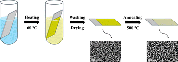
Solution A was prepared by dissolving 6.6 g Na2WO4·2H2O in 100 mL deionized water (DI water). Solution B was formulated by dissolving 3.6 g of H2C2O4 in 100 mL DI water. For the chemical bath deposition, 0.5 mL of both solution A and B were transferred to a 12 mL polypropylene centrifuge tube. The mixture was diluted to 3 mL with DI water, followed by addition of 2 mL HCl (2 M) to achieve a final pH < 1. The FTO glass was positioned in the reaction tube with the conductive surface facing downward against the tube wall. The sealed reaction system was kept in a preheated metal heating block maintained at 60 °C for 3 h. After the reaction time, the synthesized H2WO4/FTO samples were taken out immediately and rinsed with DI water and ethanol several times to remove the residual reactants. Then it was dried at 60 °C for 12 h and marked as H5. Thermal conversion to WO3/FTO was achieved through calcination in a muffle furnace at 500 °C for 3 h, inducing a chromatic transition from light yellow to pale white; the annealed specimen was labeled as W5 (Fig. 1). A series of samples was fabricated by similar steps except for systematically varying the volume of solution B; these were named H1 to H9 before annealing and W1 to W9 after annealing. Full parametric details are shown in Table S1 in the SI.2.3 Characterization
The structure of the as-prepared H2WO4/FTO and WO3/FTO samples were characterized by XRD (SmartLab SE, Rigaku, Japan) using a Cu Kα radiation (λ = 0.15418 nm) over a 2θ range from 10° to 70° at a scan rate of 10° min−1. The morphology and microstructure were observed using a scanning electron microscope (FESEM, GeminiSEM 360, ZEISS, Germany). The bonding configurations and charge transfer process of the products were determined with X-ray photoelectron spectroscopy measurements (XPS, AXIS SUPRA+, SHIMADZU, Japan), the binding energies of the tested elements were adjusted based on the indefinite carbon peak at 284.8 eV. The optical transmittance of the samples was measured using a UV-vis spectrophotometer (N4S, INESA, China). The electrochemical measurements were carried out on an electrochemical workstation (CS2350M, Wuhan Corrtest Instrument, China) using a three-electrode system consisting of a standard Ag/AgCl electrode as the reference electrode (RE), a platinum plate as the counter electrode (CE) and the fabricated WO3/FTO as the working electrode (WE) in 0.5 M H2SO4. The in situ electrochromic test was carried out by combing the spectrophotometer and electrochemical workstation above. It was carried out in a 0.1 M LiClO4/PC with a two-electrode system consisting of a platinum plate as the counter electrode and the as-prepared WO3/FTO as the working electrode.3 Results and discussion
3.1 Composition and structure
Fig. 2 displays the XRD patterns of the as-prepared H2WO4 and WO3 samples. As depicted in Fig. 2a, all H series samples matched the H2WO4 phase (JCPDS No. 43-0679). A peak at 16.4°, corresponding to the (020) plane, showed an increasing trend from H1 to H9. Meanwhile, the peak at 25.6°, associated with the (111) plane, increased from H1 to H5 and then decreased. Another notable peak at 34.0°, corresponding to the (200) plane, increased from H1 to H6 before decreasing. The varying peak intensities indicated that controlling the addition of H2C2O4 altered the preferential growth direction of the H2WO4 nanosheets. Our previous research confirmed that the exposed facet of H2WO4 nanosheets prepared by this method was the (020) plane. The peaks at 26.4° were attributed to FTO; a higher intensity suggested a thinner H2WO4 film. Notably, H1 and H9 in Fig. 2a were particularly thin.In Fig. 2b, all W series samples matched the WO3 phase (JCPDS No. 43-1035). The three peaks located between 20° to 25° are characteristic peaks of WO3, indexed to the (002), (020), and (200) planes, respectively. The peak intensity of the (002) plane increased with the addition of H2C2O4, reaching its maximum in sample W5. Another peak, located at 34.1° and indexed to the (202) plane, showed a significant change, peaking in sample W7. These peak intensities revealed a specific orientation in the as-obtained samples, indicative of a nanosheet morphology rather than bulk, as confirmed by SEM images. Additionally, comparing the peak intensities of H2WO4 with those of WO3 samples, a potential correlation can be inferred. Both the (020) plane of H2WO4 and the (002) plane of WO3 exhibited a growth trend with increasing H2C2O4 addition, suggesting that the (002) plane of WO3 may have transformed from the (020) plane of H2WO4. Similarly, the (200) and (202) planes of WO3 are likely derived from the (111) and (200) planes of H2WO4, respectively.
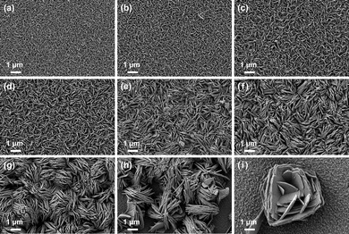
The top-view SEM images of the as-prepared H2WO4 and WO3 samples are presented in Fig. 3 and 4. Fig. 3 reveals that all samples were composed of numerous nanosheets oriented vertically to the substrate. As the concentration of H2C2O4 increased from sample H1 to H9, three major changes were observed. Firstly, the surface of the H2WO4 film in H1 was smooth, becoming progressively rougher from H1 to H6. For samples H7, H8, and H9, the thin film transitioned into distributed micro–nano islands. Secondly, by measuring 20 random nanosheets (Fig. S2), the average thicknesses of single nanosheets in samples H1 through H9 were 25.92, 31.12, 37.65, 49.37, 64.83, 84.62, 78.33, 77.65, and 82.92 nm, respectively. This trend indicates that the thickness of the nanosheets increased with the addition of H2C2O4, reaching a stable value around 80 nm. Lastly, the as-prepared H2WO4 samples exhibited a square exposed surface, with side lengths increasing from H1 to H9. The side length increased from 270 nm for H1 to 1800 nm for H9. In Fig. S2, the surface of the H2WO4 nanosheets is clearly visible, demonstrating that the thickness of the nanosheet in the H series samples increased with the increasing amount of H2C2O4. Additionally, the thicker nanosheets in H7, H8, and H9 prefer to grow from the surfaces of other nanosheets rather than the FTO substrate.
In our previous work, we successfully achieved the growth of H2WO4 nanosheets on various substrates and their self-assembly in solution. The results indicate that Na2WO4 hydrolyzes under acidic conditions to form insoluble H2WO4 precursors, which preferentially grow at hydrophilic interfaces rich in –OH. Oxalic acid, as a complexing agent, can regulate the hydrolysis rate and nucleation rate of WO4− by adjusting its concentration. In short, the higher the concentration of oxalic acid, the more WO4− participate in the oxalic acid coordination, resulting in slower hydrolysis and nucleation rates, and thinner nanosheets and thin films being formed.
Fig. 4 illustrates that the morphologies of the WO3 samples closely resemble those of the H2WO4 ones, indicating the high stability of the as-fabricated films under calcination. By measuring 20 random nanosheets from Fig. S4, the thicknesses of samples W1 through W9 were determined to be 43.09, 39.48, 48.84, 50.45, 70.79, 82.63, 84.53, 81.25, and 83.34 nm, respectively. The thicknesses of W4 through W9 were notably similar to those of H4 through H9. However, for W1, W2, and W3, the thicknesses showed a marked increase compared to H1, H2, and H3. From Fig. S4, although the morphologies of the W series samples were analogous to those of the H series, the corners of the WO3 nanosheets were less sharp than those of the H2WO4 nanosheets. Additionally, the surfaces of the WO3 nanosheets were not as smooth as those of the H2WO4 nanosheets. As observed in Fig. S4e, some concavities are present on the surface of the nanosheets, which can be categorized into two types. Point-like pores were caused by stress during the transformation of the crystal structure, resulting in surface breakage on the nanosheet surface. Rod-like pores were attributed to the detachment of nanosheets growing on the primary nanosheet substrate during the annealing process.
The thicknesses of the as-prepared WO3 films were determined using side-view SEM. Fig. 5 indicates that the FTO layer exhibited a consistent thickness across samples, confirming a uniform test environment. As shown in Fig. 5, sample W1 exhibited the thinnest thickness, approximately 370 nm. The thickness increased from W1 to W7, with the exception of W5. The W8 film demonstrated a thickness of 1120 nm. For W9, given its composition of dispersed micro–nano islands, the film structure could not be discerned in its SEM images. The SEM images further revealed that from W1 to W6, the thickness of the WO3 film was analogous to the length of its constituent nanosheets, suggesting that the film was directly composed of WO3 nanosheets growing on the FTO substrate. In the case of W7 and W8, the film comprised WO3 nanosheets growing on the FTO substrate and secondary WO3 nanosheets growing on the primary ones, which contributed to the overall increased thickness of the WO3 film.
XPS analysis was conducted to investigate the surface chemical composition and the chemical state of each element in the fabricated WO3 films. Since samples W1 through W6 displayed minimal differences in their full-spectrum and high-resolution spectra, only samples W1, W7, W8, and W9 were selected for further comparison in this section. Fig. 6a reveals characteristic signals for W and O in the full spectra of both samples, confirming the presence of WO3. However, in W9, Sn peaks were also detected, attributed to the structure of its dispersed micro–nano islands. As depicted in Fig. 6b, W1 and W7 exhibited similar W 4f and W 5p peaks, with a flat region at 27 eV, corresponding to the binding energy of Sn 4d. In W8, the intensity of the W 4f and W 5p peaks diminished, and a peak emerged at 27 eV. In W9, the peak at 27 eV was more pronounced, and the W 4f peaks shifted to lower binding energies. This phenomenon indicates a strong interaction between the FTO layer and WO3, leading to the formation of a heterojunction.
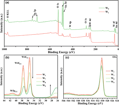 | ||
| Fig. 6 (a) Survey scan XPS spectra of W1 and W9, and the high-resolution XPS spectra for (b) W 4f and (c) O 1s of W1, W7, W8 and W9. | ||
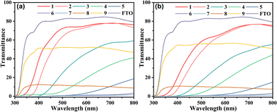
UV-Vis transmittance spectra were employed to assess the optical characteristics of the as-prepared samples. Considering their potential application in smart windows, the samples should exhibit high transmittance in their bleached state. Fig. 7a shows that the FTO-based glass demonstrated high transmittance in the visible light region, approximately 80% from 400 to 800 nm. Among all H series samples, H1 exhibited the highest transmittance, with 77% of incident light passing through from 500 to 800 nm. H2 displayed a similarly high light transmittance to H1, with a slight red shift. Subsequently, the light transmittance of the samples decreased with an increase in sample number until H7. For H8 and H9, as the films were not continuous but rather had a distributed micro–nano islands structure, these samples showed a similar transmittance trend in 300 to 800 nm to FTO with a marked decrease in transmittance.
For the WO3 samples, as shown in Fig. 7b, the UV-vis transmittance spectra revealed a high degree of similarity to those in Fig. 7a. W1 had the highest transmittance among all W series samples, followed by W2. The curves for W3 to W9 closely matched those of H3 to H9, particularly H8 and H9. This indicates that in W3 to W9, the transmittance of the entire sample was primarily determined by the large thickness of the WO3 film. In contrast, in W1 and W2, the bandgap played the main role in determining transmittance.
3.2 Electrochemical and electrochromic properties
To obtain the electrochemical characteristics of the as-prepared samples, cyclic voltammetry (CV) curves were examined at various scan rates (5, 10, 20, 50, 100 mV s−1) within the potential window of −0.3 V to 0.6 V (vs. Ag/AgCl). Upon application of an initial voltage of −0.3 V, the samples transformed into a dark blue color. As the voltage increased, the electrode materials progressively lightened. With rising scan rates, the anodic peak shifted to a more positive potential. Concurrently, the area of the curve, indicative of capacitance, broadened. This capacitive behavior can be attributed to several mechanisms, such as the adsorption of a monolayer of ions onto the electrode surface, surface redox reactions, or ion intercalation without a phase transition. In this context, the redox reaction pertains to the insertion and extraction of H+ ions and electrons within the WO3 matrix, resulting in a reversible change in transmittance between blue and yellow states as follows:| xH+ + xe− + WO3(light yellow) ⇌ HxWO3(dark blue) | (1) |
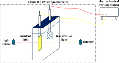
To directly examine the electrochromic properties of WO3 films, in situ UV-vis spectrometry was employed. The setup for the in situ system is shown in Fig. 9. For these tests, a 0.1 M LiClO4/propylene carbonate (PC) solution in a quartz reactor served as a blank. The samples were subjected to a voltage bias sequence of +1.0 V, followed by 0, −0.2, −0.4, −0.6, −0.8, and −1.0 V (vs. Ag/AgCl).
Fig. 10 illustrates the electrochromic performance of the W series samples. As a cathodic electrochromic material, the WO3 film can alternate its color between light yellow and dark blue under a square wave potential ranging from +1.0 V to −1.0 V in a LiClO4/PC solution. Under a negative bias, Li+ ions are inserted into the crystal lattice of WO3, causing the film to turn dark blue. Conversely, when a positive bias is applied, Li+ ions are extracted from the lattice, leading to the film's lightening. The electrochromic reaction can be described as follows:
| xLi+ + xe− + WO3(light yellow) ⇌ LixWO3(dark blue) | (2) |
The optical images of the as-prepared samples are displayed in Fig. 11. The H series samples exhibited a grayish-green hue, whereas the W series samples turned light yellow after annealing. Following the coloring process, all samples transformed into a blue color. It is evident from the images that samples H4 to H8 and W4 to W8 exhibited significant haze, as the logos and text beneath the samples were indistinct, rendering them unsuitable for smart window applications. Samples W1 and W9, while appearing uniform in the bleached state, demonstrated uneven color distribution in the colored state, revealing their heterogeneous distribution of film thickness.
 | ||
| Fig. 11 Optical images of as-prepared H2WO4/FTO, WO3/FTO samples and WO3/FTO samples after coloring. | ||
4 Conclusions
In conclusion, the mild chemical bath deposition method was employed to fabricate WO3 films on FTO substrates. By controlling the amounts of reactants, the optical properties of the WO3 films could be effectively modulated. The findings indicate that films with thinner compositions, both in terms of overall thickness and individual nanosheets, result in electrochromic films that are more transparent and flexible. The optimal samples exhibited a high degree of optical modulation, with a transmittance change (ΔT) of 67.85% at 620 nm and demonstrated good cycling stability. Furthermore, the thickness of the electrochromic films could be tuned from 370 nm to 2040 nm, show a viable approach for the large-scale production of WO3-based smart windows suitable for commercial, tunable electrochromic applications.Author contributions
J. Y.: concenptualizaion, methodology, investigation, validation, writing – original draft, supervision, funding acquisition; G. L.: methodology, investigation, resources, funding acquisition; M. Z.: methodology, investigation, resources, supervision.Conflicts of interest
There are no conflicts to declare.Data availability
The data supporting this article have been included as part of the supplementary information (SI). Supplementary information is available. See DOI: https://doi.org/10.1039/d5ma01024a.Raw data files are available from the corresponding author.
Acknowledgements
This work is supported by the Science and Technology Project of Changzhou (CJ20235011), Engineering Research Center Program of Development & Reform Commission of Jiangsu Province (Grant No. [2021] 1368).Notes and references
- X. Cao, X. Dai and J. Liu, Energy Build., 2016, 128, 198–213 CrossRef
.
- U. Berardi, Resour., Conserv. Recycl., 2017, 123, 230–241 CrossRef
.
- M. González-Torres, L. Pérez-Lombard, J. F. Coronel, I. R. Maestre and D. Yan, Energy Rep., 2022, 8, 626–637 CrossRef
.
- F. A. Dalenjan, M. Bagheri-Mohagheghi and A. Shirpay, Opt. Quantum Electron., 2022, 54, 711 CrossRef CAS
.
- J. Guo, H. Jia, Z. Shao, P. Jin and X. Cao, Acc. Mater. Res., 2023, 4, 438–447 CrossRef CAS
.
- S.-C. Hsu, S.-H. Chao, N.-J. Wu, J.-H. Huang, J.-L. Kang, H. C. Weng and T.-Y. Liu, J. Alloys Compd., 2023, 945, 169256 CrossRef CAS
.
- Q. Sun, S. Li, X. Yu, Y. Zhang, T. Liu and J. Y. Zheng, Appl. Surf. Sci., 2023, 641, 158510 CrossRef CAS
.
- S. Yu, J. Yang and C. Song, ACS Appl. Nano Mater., 2023, 6, 14948–14956 CrossRef CAS
.
- J. Gupta, H. Shaik and S. A. Sattar, J. Mater. Sci.: Mater. Electron., 2024, 35, 224 CrossRef CAS
.
- K. Usha and S. Y. Lee, Ceram. Int., 2024, 50, 23244–23255 CrossRef CAS
.
- W. Yong, N. Chen, T. Xiong and G. Fu, Mater. Today Chem., 2024, 38, 102095 CrossRef CAS
.
- J. Yu, J. Gonzalez-Cobos, F. Dappozze, F. J. Lopez-Tenllado, J. Hidalgo-Carrillo, A. Marinas, P. Vernoux, A. Caravaca and C. Guillard, Appl. Catal., B, 2022, 318, 121843 CrossRef CAS
.
- Y. Chen, J. Sun, Y. Huang, D. Lin, D. Ma and J. Wang, Ceram. Int., 2023, 49, 29534–29541 CrossRef CAS
.
- J. Y. Zheng, Z. Haider, T. K. Van, A. U. Pawar, M. J. Kang, C. W. Kim and Y. S. Kang, CrystEngComm, 2015, 17, 6070–6093 RSC
.
- R. Yu, Z.-H. Meng, M.-D. Ye, Y.-H. Lin, N.-B. Lin, X.-Y. Liu, W.-D. Yu and X.-Y. Liu, CrystEngComm, 2015, 17, 6583–6590 RSC
.
- F. Zheng, W. Man, M. Guo, M. Zhang and Q. Zhen, CrystEngComm, 2015, 17, 5440–5450 RSC
.
- S. Wang, H. Xu, J. Zhao and Y. Li, Inorg. Chem. Front., 2022, 9, 514–523 RSC
.
- J. Su, L. Chen, C. Xu, Y. Liu, L. Shen and Z. He, J. Mater. Chem. A, 2024, 12, 29383–29401 RSC
.
- C. Gao, X. Guo, X. Wu, L.-M. Peng and J. Chen, Cryst. Growth Des., 2023, 23, 4410–4416 CrossRef CAS
.
- J. Kim, S. Choi, S. Kim, W. Liu, M. Wang, X. Diao and C. S. Lee, Electrochim. Acta, 2023, 472, 143394 CrossRef CAS
.
- J. Yao, P. Li and X. Liu, J. Cryst. Growth, 2023, 601, 126947 CrossRef CAS
.
- C.-M. Chang, Y.-C. Chiang, M.-H. Cheng, S.-H. Lin, W.-B. Jian, J.-T. Chen, Y.-J. Cheng, Y.-R. Ma and K. Tsukagoshi, Sol. Energy Mater. Sol. Cells, 2021, 223, 110960 CrossRef CAS
.
- X. Zhang, S. Dou, W. Li, L. Wang, H. Qu, X. Chen, L. Zhang, Y. Zhao, J. Zhao and Y. Li, Electrochim. Acta, 2019, 297, 223–229 CrossRef CAS
.
- W. Zhang, H. Li, E. Hopmann and A. Y. Elezzabi, Nanophotonics, 2020, 10, 825–850 CrossRef
.
- Z. Wang, X. Wang, S. Cong, J. Chen, H. Sun, Z. Chen, G. Song, F. Geng, Q. Chen and Z. Zhao, Nat. Commun., 2020, 11, 302 CrossRef CAS PubMed
.
- J.-L. Wang, J.-W. Liu, S.-Z. Sheng, Z. He, J. Gao and S.-H. Yu, Nano Lett., 2021, 21, 9203–9209 CrossRef CAS PubMed
.
- B. Zhang, J. Luo, Z. Chen, L. Wu, J. Li, Y. Tian and S. Liu, J. Electroanal. Chem., 2022, 918, 116487 CrossRef CAS
.
- L. Li, M. Hu, C. Hu, B. Li, S. Zhao, T. Zhou, J. Zhu, M. Liu, L. Li and J. Jiang,
et al.
, Nano Lett., 2023, 23, 7297–7302 CrossRef CAS PubMed
.
- Z. Mei, M. Wang, Y. Ding and X. Diao, Vacuum, 2023, 214, 112219 CrossRef CAS
.
- A. C. Nwanya, C. J. Jafta, P. M. Ejikeme, P. E. Ugwuoke, M. Reddy, R. U. Osuji, K. I. Ozoemena and F. I. Ezema, Electrochim. Acta, 2014, 128, 218–225 CrossRef CAS
.
- M. Z. Najdoski and T. Todorovski, Mater. Chem. Phys., 2007, 104, 483–487 CrossRef CAS
.
- F. Zhao, Y. Zeng, Z. Cheng, G. Shi, Q. Liu, Y. Liu and G. Han, Chem. Eng. J., 2024, 485, 149350 CrossRef CAS
.
- S. Wang, T. Jiang, Y. Meng, R. Yang, G. Tan and Y. Long, Science, 2021, 374, 1501–1504 CrossRef CAS PubMed
.
- D. Zou, T. Xu, H. Li, X. Zhang, H. Sun, Q. Rao, M. Zhu, S. Chang, Y. He and H. Meng, ACS Appl. Mater. Interfaces, 2025, 17, 21736–21744 CrossRef CAS PubMed
.
- P. A. Shinde, V. C. Lokhande, N. R. Chodankar, T. Ji, J. H. Kim and C. D. Lokhande, J. Colloid Interface Sci., 2016, 483, 261–267 CrossRef CAS PubMed
.
| This journal is © The Royal Society of Chemistry 2026 |

