
Micro–nano surface engineering and property modulation: insights from black silicon for advanced material applications
Junling
Lv
 a,
Lihong
Jiang
a,
Xinlin
Liu
a,
Gaojie
Li
a,
Mingrui
Qian
b,
Mingxin
Tang
a,
Xinao
Cheng
b,
Lan
Lu
a,
XiaRong
Ren
a,
Xueling
Zhang
a,
Haiyang
Zou
*a and
Zhong Lin
Wang
*cd
a,
Lihong
Jiang
a,
Xinlin
Liu
a,
Gaojie
Li
a,
Mingrui
Qian
b,
Mingxin
Tang
a,
Xinao
Cheng
b,
Lan
Lu
a,
XiaRong
Ren
a,
Xueling
Zhang
a,
Haiyang
Zou
*a and
Zhong Lin
Wang
*cd
aCollege of Materials Science and Engineering, Sichuan University, Chengdu 610065, China. E-mail: zhy@scu.edu.cn
bCollege of Biomedical Engineering, Sichuan University, Chengdu 610065, China
cSchool of Nanoscience and Engineering, University of Chinese Academy of Sciences, Beijing 100049, P. R. China
dSchool of Materials Science and Engineering, Georgia Institute of Technology, Atlanta, GA 30332, USA. E-mail: zlwang@gatech.edu
First published on 19th March 2026
Abstract
The advancement of micro–nano fabrication techniques has enabled the precise modification of material surfaces, allowing for unique physical and chemical properties to emerge, catering to diverse application requirements. Black silicon, a well-studied material compatible with CMOS technology, provides an excellent model for exploring the overall properties of micro–nano surface morphologies. This review systematically investigates the morphology fabricated by five mainstream synthesis methods for black silicon, offering an in-depth analysis of the underlying mechanisms and the impact of key parameters on surface morphology. In addition to structural features, this review discusses the formation of surface chemical bonds and their roles in modulating surface energy, wettability, and electronic passivation. Through this exploration, we examine how specific morphologies yield distinct physical and chemical properties that drive a wide range of applications, from photodetection to sensing and biomedical technologies. Key challenges of black silicon are discussed, including cost, mass production, and defect control, etc. This review aims to serve as a roadmap for researchers, guiding further advancements not only in black silicon but also in the broader field of nanomaterials, paving the way for breakthroughs across various domains of modern nanotechnology.
 Junling Lv | Junling Lv received her bachelor's degree in Materials Science and Engineering from Sichuan University in 2023. She is continuing to pursue her PhD degree at Sichuan University. Her research interests are mainly focused on the alternating current photovoltaic effect and its applications. |
 Haiyang Zou | Dr Haiyang Zou is currently a Professor at the College of Materials Science and Engineering at Sichuan University. Holding a PhD degree from the esteemed Georgia Institute of Technology, USA, he furthered his expertise through postdoctoral research there. Dr Zou's academic journey has led him to specialize in a wide array of areas including nanomaterials, nano-systems, and nano-devices, as well as photonics, piezo-electronics, piezo-phototronics, triboelectric nanogenerators, and flexible electronics. He was recognized as one of the world's most influential researchers in his field based on the databases of standardized citation indicators (the world's top 2% scientists named by Stanford University). |
 Zhong Lin Wang | Zhong Lin Wang is the Hightower Chair in Materials Science and Engineering, Regents' Professor, and College of Engineering Distinguished Professor at the Georgia Institute of Technology. He is now the director of the Beijing Institute of Nanoenergy and Nanosystems. Prof. Wang has made original and innovative contributions in the fields of oxide nanobelts and nanowires, piezotronics and piezo-phototronics as well as their applications in energy sciences, electronics, optoelectronics and biological science. Dr Wang was elected as a member of the Chinese Academy of Sciences and European Academy of Sciences, an academician of the Academia of Sinica (Taiwan), and an international fellow of the Canadian Academy of Engineering. |
1. Introduction
The rapid progression of micro–nano fabrication technologies has ushered in transformative capabilities for tailoring material surfaces to enhance or modify physical, chemical, and electronic properties.1–3 These advancements play a vital role in developing materials for applications that demand high specificity, sensitivity, and adaptability. Among various materials, silicon has long been a cornerstone of the electronic and optical device industries, primarily due to its compatibility with CMOS technology, robust mechanical properties, and well-understood electronic characteristics. As the demand for more efficient and versatile devices grows, the limitations of conventional silicon structures become increasingly apparent.4–7Black silicon is typically structured with nanometer- to micrometer-scale features,8 such as holes, needles, and columnar formations, and it exhibits properties not found in conventional silicon surfaces. The advent of black silicon, an optically and chemically modified form of silicon, has expanded silicon's applicability beyond conventional electronics. Black silicon demonstrates exceptional photon capture and confinement abilities, owing to its significantly increased active surface area and quantum confinement effects.9–11 This transition from a traditional, smooth surface to one rich with nanoscale and microscale structures fundamentally transforms silicon's interaction with light, fluids, and biological elements. Its unique surface morphology, often achieved through tailored micro–nano structuring, imbues black silicon with extraordinary properties such as enhanced light absorption,12,13 superhydrophobicity,14,15 and augmented chemical reactivity.16–18 These characteristics make black silicon particularly suitable for a range of applications in photodetection,19–21 solar cells,22,23 sensors,24–26 biomedical devices,27–32 and environmental monitoring.33 However, realizing these properties and applications hinges significantly on the precise control of black silicon's morphology,34,35 which can vary substantially depending on the synthesis method employed. Therefore, it is crucial to study the surface morphology of black silicon and explore how morphological features influence various material and device performances.
In recent years, there has been a growing trend of research articles and reviews focusing on black silicon.8,9,36–40 Existing reviews have primarily focused on fabrication innovations and specific applications. Liu et al. summarized the fabrication methods and photoelectric properties of black silicon, as well as the applications and improvements in solar energy utilization.8 Martin et al. provided guidelines for optimising the relevant parameters for better optoelectronic applications.41 Zhao et al. offered an in-depth review of the morphology and mechanisms of laser etching to fabricate black silicon, with a focus on its applications and future directions in infrared detection.39 Other reviews have explored topics such as biomaterials,42 battery anodes43,44 and antibacterial surfaces.40 However, a comprehensive analysis of black silicon's surface morphology remains insufficient, especially its evolution under different fabrication strategies and its direct influence on material properties (e.g., physical, chemical, and biological properties). The surface architecture, including micro- and nanoscale features such as spikes, pores, and trenches, critically affects light trapping, carrier dynamics, and interfacial behaviors. Moreover, the formation of specific chemical bonds (e.g., Si–H, Si–O, and Si–F) during fabrication also modulates surface energy and states, leading to various properties. Therefore, a systematic review that unifies the morphological characteristics of black silicon with its fabrication-dependent chemical and physical properties is essential. Such a perspective is crucial for understanding its fundamental mechanisms and for guiding the rational design of high-performance black silicon-based devices across diverse applications.
In this review, we aim to provide a comprehensive roadmap for future advancements in micro–nano surface engineering. By examining the relationship between morphology and functionality, we seek to deepen the understanding of how surface morphology and chemical states can be tailored to achieve desired material properties and meet specific application requirements. This paper begins by tracing the evolution of fabrication methods, followed by a detailed analysis of key fabrication techniques, such as chemical etching, reactive ion etching (RIE), metal-assisted chemical etching (MACE), laser etching, and plasma immersion ion implantation etching (PIIIE), to elucidate the mechanisms and factors influencing the morphology of black silicon. This review also investigates how surface chemical bonding states formed during fabrication, in conjunction with morphological features, collectively influence surface energy, surface physicochemical properties, and interfacial electronic characteristics. The interplay between morphology and surface chemistry is critical for optimising light trapping, carrier dynamics, and environmental stability. By correlating fabrication methods, surface morphology, chemical terminations, and material properties, this review provides key insights for the rational design of black silicon devices and identifies both the challenges and opportunities for their broader application. The scope and structure of this review are depicted in Fig. 1. This comprehensive analysis serves as a valuable resource for researchers and engineers seeking to navigate the complexities of black silicon fabrication and offers practical guidance for overcoming the barriers to its broader application. Moreover, our analysis not only applies to black silicon but may also inform research on other nanostructured materials, ultimately contributing to the broader field of nanotechnology and its myriad applications.
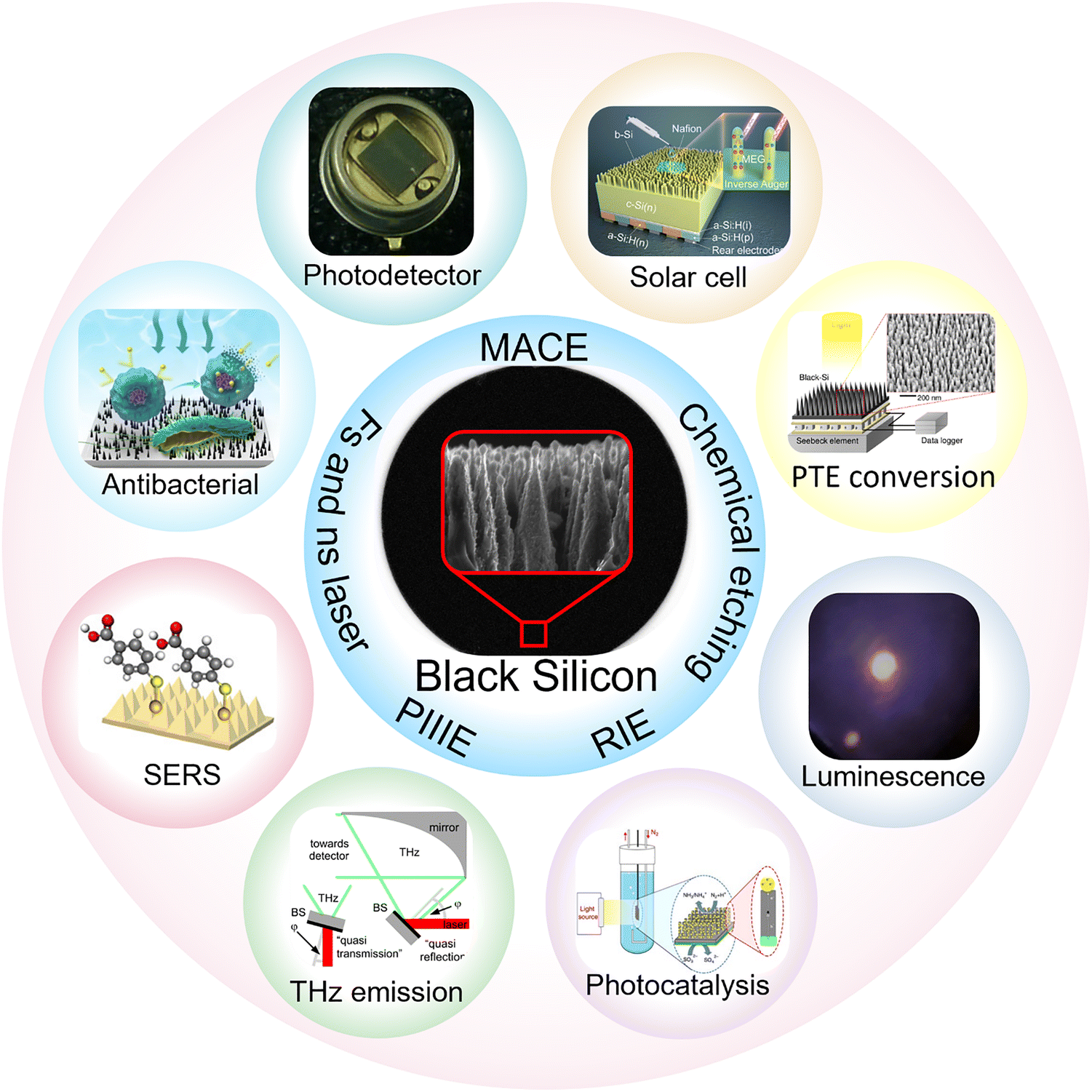 | ||
| Fig. 1 The wide applications of black silicon: photodetectors,45 solar cells,46 PTE conversion,47 luminescence,48 photocatalysis,49 THz emission,50 SERS,51 and antibacterial.34 | ||
2. Micro–nano engineering strategies for morphology control
The fabrication history of black silicon can be traced back to 1959.52 At that time, silicon was immersed in an etchant solution consisting of hydrofluoric acid (HF), nitric acid (HNO3), and water (H2O) at 25 °C to study the kinetics of silicon etching under acidic conditions. In 1995, a significant milestone was achieved when RIE was employed to fabricate black silicon. The term “black silicon” was coined to describe the distinctly darkened surface of the etched silicon.53 The resulting morphology consisted of grass-like nanostructures formed on the silicon surface. Based on chemical etching, the metal particles were introduced to accelerate the etching process, and more regular structures could be achieved by this method, which was named MACE.54 It wasn’t until 1998 that Eric Mazur et al. prepared sulfur-doped black silicon by femtosecond laser irradiation under a sulfur hexafluoride (SF6) atmosphere,55 expanding the light absorption range beyond 1100 nm. After doping sulfur to form a supersaturated doped silicon, the introduced impurities formed a new energy band structure, effectively broadening the light absorption range. Another doping method to fabricate black silicon, PIIIE appeared in 2011,22 the needle-like surface reduced the average reflectance to 1.79% in the range of 300–1100 nm. Some important improvement milestones of the five fabrication methods are shown in Fig. 2 and discussed as follows.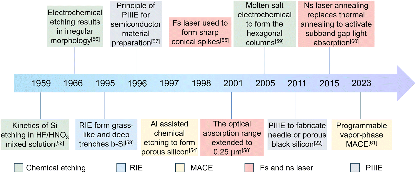 | ||
| Fig. 2 The development timeline of various black silicon fabrication methods, including several key milestones.22,52–61 | ||
Porous silicon was first discovered at Bell Laboratories in 1956 through electrochemical etching,62 but initially garnered little interest due to its defective surface properties. A decade later, in 1966, Memming et al. investigated the factors influencing silicon dissolution, such as electrode potential, crystal doping, and HF concentration,56 although the technique did not produce a regular surface morphology at the time. In 1959,52 etching with pure acid solution was introduced, marking a new approach. In 2005, the development of molten salts’ electrochemical etching enabled the direct electrolytic reduction of solid silicon dioxide (SiO2) to silicon, resulting in more uniformly structured hexagonal silicon columns.59 This method proved to be a more economical and efficient approach for fabricating black silicon.
RIE was first applied to silicon by Jansen in 1995,53 demonstrating its versatility in creating nanograss and enabling the formation of vertical walls. This capability allows for precise control over silicon nanostructures through parameter adjustments. In 2012, sputtered silver nanoparticles (AgNPs) were introduced as micromasks,63 replacing the SiO2 layer that was previously formed by oxygen (O2) and served as a random micro-mask. This substitution reduced the need for O2 in the process, thereby minimizing damage and prolonging the lifespan of black silicon. Researchers also examined the effects of AgNPs and etching duration on surface characteristics. Nguyen et al. later conducted an in-depth study on how RIE parameters affect the surface morphology of black silicon,64 establishing a relationship between optical properties and the aspect ratio of micro–nano structures, which further refined the controllability of RIE in black silicon fabrication. To create more regular microstructures, masks have been employed to control the spatial distribution of the etched features, enabling the development of hierarchical micro–nano hybrid structures that further enhance light absorption.65 In recent advancements, black silicon has been successfully fabricated on curved surfaces,66 and ultrabroadband absorption extending to 20 µm was achieved in 2023,67 highlighting the promising future of RIE in black silicon technology.
MACE was developed by adding metal nanoparticles as catalysts during chemical etching, mostly noble metal nanoparticles. The initial MACE formed porous silicon by depositing aluminum (Al) thin films in 1997,54 then the influence of different types of metal nanoparticles, silicon types, and doping levels was investigated by Li et al.68 Koynov et al. demonstrated that black silicon prepared by MACE is independent of surface orientation, making the process applicable to various types of silicon, including monocrystalline, polycrystalline, amorphous, and thin films.69 Similar to RIE, masks were also widely employed in MACE.70 Metal nanoparticles were deposited on the unmasked regions, so micro–nanostructures are selectively formed in these areas. This approach facilitates the creation of regular and controllable nanowire arrays, enhancing the uniformity of the etched structures. The influence of annealing temperature on the morphology and optical properties of black silicon has also been concluded,71 showing clear benefits for the performance of photovoltaic devices. A recent study reported a gas-phase programmed MACE technique,61 which effectively addresses the long-standing issue of large-area etching nonuniformity and provides a new strategy for the further development of MACE technology.
One advantage of femtosecond and nanosecond laser irradiation over other methods is its ability to incorporate doping during preparation, effectively broadening the light absorption range in black silicon. Since the pioneering work of Mazur's group,55 this technique has attracted significant research interest. Wu et al. expanded the light absorption range of femtosecond-laser-fabricated black silicon to 0.25 µm while maintaining over 90% absorption, and they further provided insights into the underlying infrared absorption mechanism.58 Subsequent studies have explored various factors affecting laser etching, including background gas composition,72,73 laser pulse numbers,74 laser fluence and scanning speed,75 as well as annealing and substrate temperatures.76 In 2011, a direct femtosecond laser surface structuring method was developed to create a velvet-like surface morphology with outstanding antireflective properties.77 Recognizing that thermal annealing can deactivate sub-bandgap light absorption, laser annealing has emerged as a promising alternative. It preserves high crystallinity while reactivating sub-bandgap absorption.60 Additionally, combining femtosecond laser irradiation with other fabrication methods has been shown to significantly enhance the performance of black silicon.78,79
PIIIE is another innovative method to fabricate black silicon. Although the mechanism was reported as early as 1996,57 its application to silicon was not demonstrated until 2011.22 Since then, numerous studies have explored the factors affecting the process.80,81 Lim et al. optimized the process by using environmentally friendly plasmas instead of SF6 and O2, which were commonly used in the past.82 This approach not only reduced environmental impact but also passivated surface defects and enabled the production of ultra-low reflectivity black silicon.
The subsequent sections will provide a detailed examination of each fabrication method, including the mechanisms involved and the various factors that influence surface morphologies.
2.1. Chemical etching
Chemical etching is an appealing technique widely used for black silicon fabrication, offering control over surface morphology and optical properties by selectively removing silicon through chemical reactions. This method includes several types, each with distinct characteristics, etching depths, and applications. In general, pure chemical etching in acidic or alkaline solutions produces relatively shallow texturing at the nanometer to submicronmeter scale, primarily forming random porous or pyramidal structures. Electrochemical etching, in contrast, enables the fabrication of porous silicon with well-defined pore networks that can extend to several micrometers in depth, making it more suitable for sensing and catalytic applications. Electrochemical etching in molten salts represents a more recent development and can produce even deeper and more uniform columnar structures through the high-temperature electrolytic reduction of SiO2. These differences in etching depth and morphology directly influence the light-trapping ability and optoelectronic performance of black silicon. Therefore, it is important to distinguish the modalities when evaluating their potential applications.In acidic chemical etching, HF and nitric acid (HNO3) are commonly used. The etching process is a redox reaction,52 where HNO3 oxidizes the silicon surface and HF subsequently dissolves the resulting oxides. The overall reaction for acidic etching can be expressed by eqn (2.1)
| 3Si + 12HF + 4HNO3 → SiF4 + 4NO + 8H2O | (2.1) |
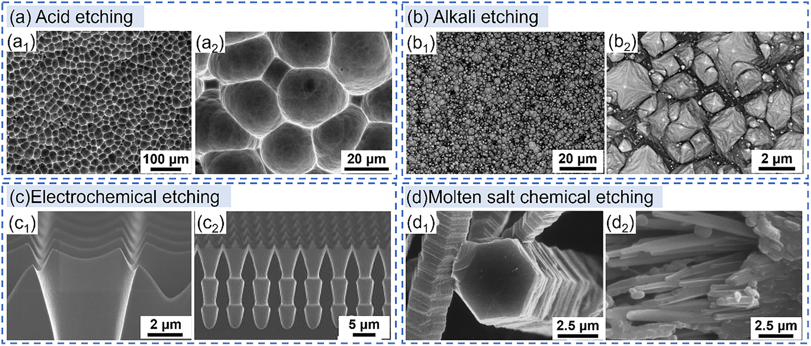 | ||
| Fig. 3 SEM images of black silicon morphologies produced by different chemical etching methods. (a) HF/HNO3 acidic etching.83 Reproduced with permission from ref. 83. Copyright 2009, Elsevier. (b) Alkaline KOH/IPA etching.84 Reproduced with permission from ref. 84. Copyright 2021, MDPI. (c) Electrochemical etching.85 Reproduced with permission from ref. 85. Copyright 2012, AIP Publishing. (d) Silicon columns obtained by molten CaCl2 etching at 1123 K.59 Reproduced with permission from ref. 59. Copyright 2005, IOP Publishing. | ||
For alkaline chemical etching, solutions containing sodium hydroxide (NaOH), potassium hydroxide (KOH), isopropanol (IPA), or their mixtures are commonly used. The mechanism can be expressed by eqn (2.2) and (2.3) as follows. Furthermore, the etching rate and the resulting surface morphology can be effectively controlled by adjusting the concentrations of the alkaline components.
| Si + 4OH− → SiO42− + 2H2 | (2.2) |
| SiO42− + 4H2O → Si(OH)4 + 4OH− | (2.3) |
To facilitate a concise quantitative comparison between acidic and alkaline chemical etching, representative characteristics are summarized in Table 1. Acidic etching is generally associated with higher, largely isotropic etching rates, giving rise to porous or pit-dominated surfaces with relatively high roughness and broad feature-size distributions. In contrast, alkaline etching is characterized by lower but strongly anisotropic etching behavior, typically exhibiting etching rate ratios between 〈100〉 and 〈111〉 directions exceeding one order of magnitude. This pronounced anisotropy enables the formation of well-defined pyramidal morphologies with improved surface uniformity and reduced optical reflectance, which are particularly advantageous for photovoltaic applications.
| Metric | Acidic chemical etching | Alkaline chemical etching |
|---|---|---|
| Etching anisotropy | Isotropic | Strongly anisotropic |
| Crystal-plane dependence | Weak | Strong (〈100〉 ≫ 〈111〉) |
| Characteristic morphology | Porous/pit-dominated | Upright or inverted pyramids |
| Feature size scale | Micro- to nanoscale mixed | Micrometer-scale |
| Surface roughness | Relatively high | Relatively low |
| Typical applications | Light trapping, sensing | Photovoltaics, wafer thinning |
Despite the advantages of pure chemical etching, including its simplicity, good selectivity, and suitability for mass production, this method struggles to produce highly regular microstructures. As a result, its applications are somewhat constrained. To overcome these limitations, pure chemical etching is often combined with metal nanoparticles to achieve more precise structural control. This process will be discussed in detail in Section 3.3.
| Si + 2H2O → SiO2 + H2 + 2H+ + 2e− | (2.4) |
| SiO2 + 6HF → 2H+ + SiF62− + 2H2O | (2.5) |
As the H+ concentration increases in the HF solution, the silicon oxidation rate decreases, allowing fluorine ions to etch the silicon surface layer by layer.89 Additionally, the doping concentration and dopant type of silicon significantly influence the etched microstructure: antimony (Sb)-doped wafers produce high-density, tall, and narrow conical structures with deep clefts, resulting in a blacker surface appearance than phosphorus (P)-doped wafers, which create thicker cones with sharper tips.90
Etching potential also influences silicon's etching characteristics.56,91 At lower potentials, oxide formation is slower than oxide dissolution, thus preventing the formation of an oxide film. With an increase in potential, porous silicon formation accelerates, particularly at higher HF concentrations. At even higher potentials, oxidation dominates, and once the potential reaches peak current, a uniform oxide film coats the surface. This initiates a continuous cycle of oxide formation and dissolution, leading to uniform electropolishing across the silicon surface.
Conventional chemical etching typically produces irregular surfaces; however, by pre-treating specific areas on the silicon surface, the etching process can be controlled to form regular microstructures. In a study by Ao et al.,85 a hexagonal pattern of inverted pyramidal pits was formed on n-type silicon by photolithography to guide the growth of holes. The aperture was adjustable by varying the current density at the silicon/HF interface for a given interpore distance and under fixed etching conditions. Scanning electron microscope (SEM) images of these structured etchings are shown in Fig. 3(c). Compared to pure chemical etching, electrochemical etching facilitates the formation of regular microstructures more easily and achieves a higher etching rate.
Yasuda et al. investigated the mechanism of direct electrolytic reduction of SiO2 in molten calcium chloride (CaCl2),59 where the total reaction can be represented in eqn (2.6):
| SiO2 + 4e− → Si + 2O2− | (2.6) |
In summary, chemical etching offers versatile routes for black silicon fabrication, with each modality presenting unique advantages and limitations. Rather than a universally optimal approach, the choice of etching method enables a balance between structural uniformity, scalability, and optical performance. These distinctions not only guide the selection of suitable techniques for specific applications but also point to the potential of hybrid strategies for achieving more advanced black silicon architectures.
2.2. Reactive ion etching
RIE is a plasma-based etching method that enables the formation of various silicon surface morphologies by precisely controlling plasma parameters. RIE is typically performed within inductively coupled plasma (ICP) or capacitively coupled plasma (CCP) systems, shown in Fig. 4.94 This technique can produce a range of structures, including isotropic surfaces, reverse tapers, and vertical walls.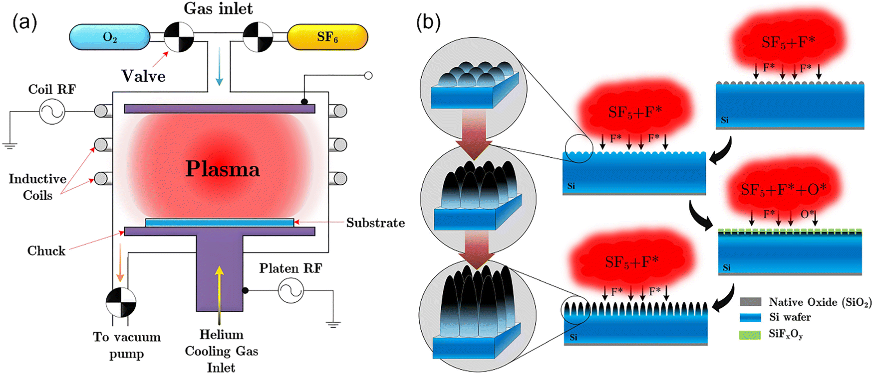 | ||
| Fig. 4 The equipment and mechanisms of RIE.94 Reproduced with permission from ref. 94. Copyright 2017, AIP Publishing. (a) Schematic of the ICP and CCP system used for the RIE process. (b) Schematic view of RIE in SF6/O2 plasma. | ||
In the initial application of RIE on silicon by Jansen et al., silicon wafers were etched to create grass-like microstructures using a plasma mixture of SF6, O2, and trifluoromethane (CHF3), each gas playing a specific role in the etching process.53 The primary functions include chemical etching, passivation, and selective layer removal, which together enable the formation of intricate micro- and nanostructures. The following is a breakdown of these functions and the associated reactions: (1) SF6 produces fluorine radicals (F*), which chemically etch silicon by forming volatile sulfur tetrafluoride (SF4). (2) O2 generates oxygen radicals (O*), which passivate the silicon surface with a SiOxFy layer that forms at cryogenic temperatures and volatilizes at room temperature. This SiOxFy layer prevents the silicon from further chemical corrosion, although it can be dissociated by heat or plasma ion bombardment, enabling the formation of controlled, intricate surface structures. (3) CHF3 produces CFx+ ions that selectively etch the SiOxFy layer in one direction, creating volatile COxFy compounds. (4) SFx+ ions aid in removing the oxyfluoride layer by forming volatile SOxFy gases. The overall etching process follows these reactions in eqn (2.7)–(2.10):95
| Si + 4F* → SiF4↑ | (2.7) |
| SiFy+ + xO* → SiOxFy | (2.8) |
| SiOxFy + CFx+ → COxFy↑ | (2.9) |
| SiOxFy + SFx + → SOxFy↑ | (2.10) |
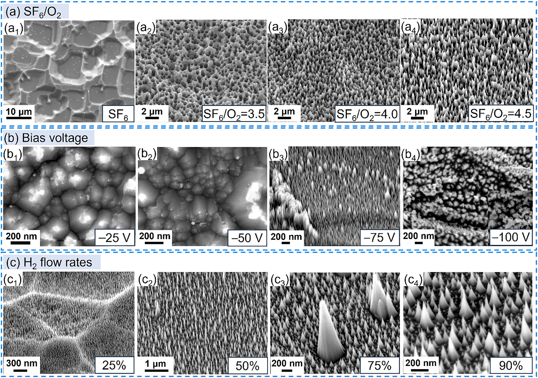
The key influencing factors of RIE include radio frequency (RF) powers, etching time, gas composition, chamber pressure, and gas flow rate, each affecting the properties of black silicon in distinct ways.96 ICP or RF power directly impacts surface morphology, with higher power levels increasing the frequency of ion bombardment, which results in taller structures; however, there is an upper limit to this effect.97 The etching time has been studied under a constant working pressure of 2 Pa with SF6 and O2 flows at 60 sccm, as shown in Fig. 5(a).95 Over time, the black silicon surface becomes progressively rougher; after 1.5 min, independent etching pits begin to appear, marking the onset of anisotropic etching. As etching continues, vertical pores deepen, widen, and connect, with interconnection nearly complete after approximately 3 min. By the 5-minute mark, the entire surface exhibits interconnected pores, effectively reducing reflectivity. Extending the etching time further increases pore width and depth, though pore length is ultimately limited by the aspect ratio-dependent etching effect.97
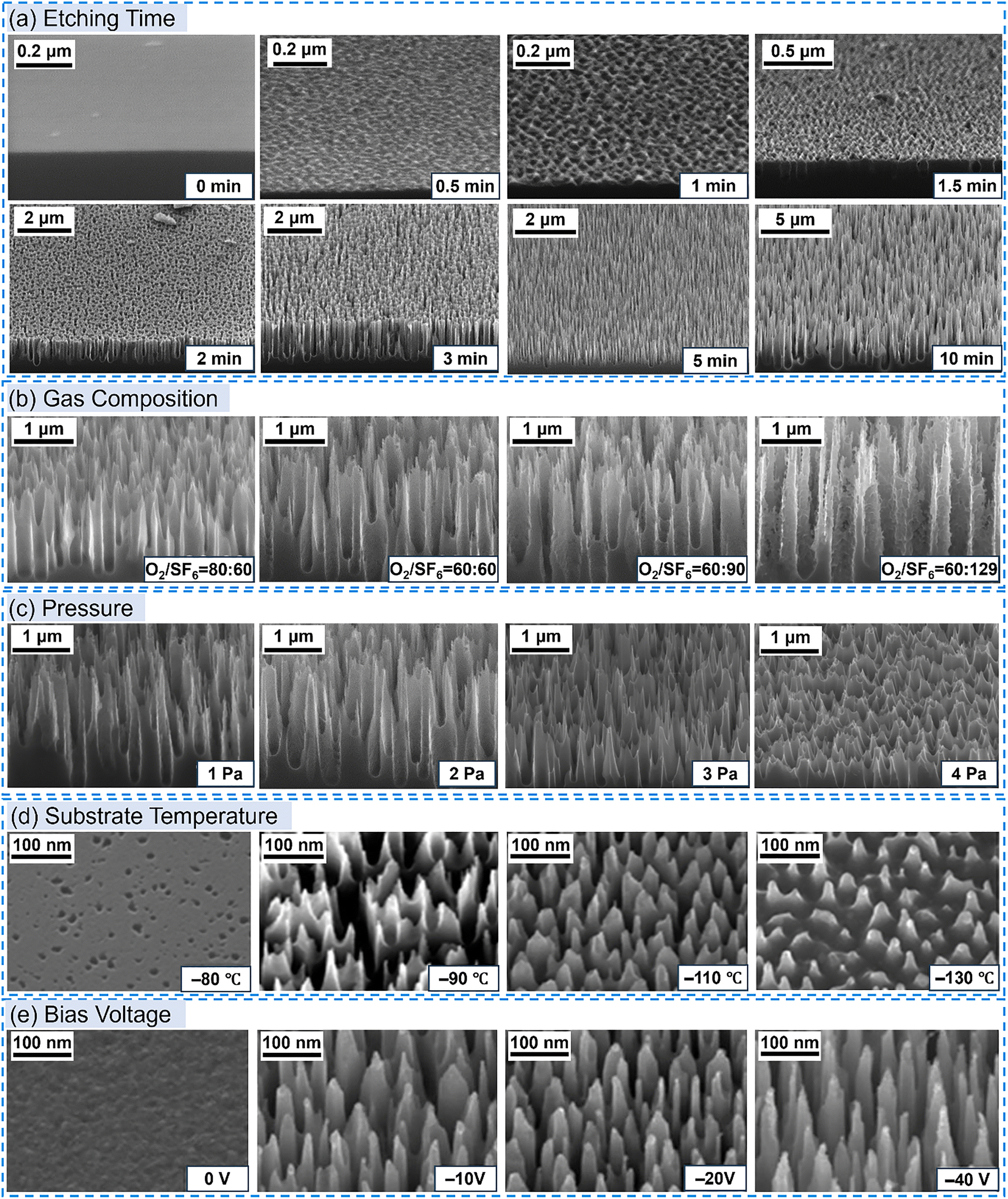 | ||
| Fig. 5 SEM images showing the effects of different RIE parameters on black silicon morphology. (a) Etching time. (b) Gas composition. (c) Pressure.95 Reproduced with permission from ref. 95. Copyright 2014, AIP Publishing. (d) Substrate temperature. (e) Bias voltage.64 Reproduced with permission from ref. 64. Copyright 2013, AIP Publishing. | ||
By adjusting the concentrations of SF6 and O2, various surface structures can be tailored to meet specific profile requirements.95 Higher SF6 concentrations or lower O2 levels promote more isotropic structures, while increasing O2 levels result in positively tapered, conical profiles. Plasma gas composition plays a crucial role in determining surface morphology, as shown in Fig. 5(b), which illustrates SEM images for O2/SF6 gas flow ratios of 80![[thin space (1/6-em)]](https://www.rsc.org/images/entities/char_2009.gif) :60, 60:60, 60:90, and 60:129. As the SF6 concentration increases, the sidewalls of the microstructure show more fraying due to the formation of shallow nanopores. Conversely, O2 contributes a passivation effect, and higher O2 content reduces both the width and depth of the apertures. Additionally, process pressure significantly impacts nanoscale morphologies by modulating the energy and directionality of ions impinging on the surface, providing further control over the etching process.
:60, 60:60, 60:90, and 60:129. As the SF6 concentration increases, the sidewalls of the microstructure show more fraying due to the formation of shallow nanopores. Conversely, O2 contributes a passivation effect, and higher O2 content reduces both the width and depth of the apertures. Additionally, process pressure significantly impacts nanoscale morphologies by modulating the energy and directionality of ions impinging on the surface, providing further control over the etching process.
The impact of process pressure on etched morphologies is significant, influencing the depth and sidewall profiles of the resulting structures.95 As shown in Fig. 5(c), the morphologies at pressures of 1 Pa and 2 Pa are similar, characterized by slender structures with nanopores on the sidewalls. However, as the pressure increases to 3 Pa and 4 Pa, the depth of the structures decreases, and the sidewalls become less steep. This change can be attributed to the reduced mean free path of ions at higher pressures, which limits their acceleration and suppresses anisotropic etching. Instead, isotropic etching is enhanced, resulting in a more uniform etching profile. Consequently, the positive sidewall effect preserves more etch pores, leading to shorter and smaller nanostructures.
Substrate temperature significantly impacts surface morphology by affecting the formation of the SiOxFy passivation layer.64 As shown in Fig. 5(d), at −80 °C, the surface appears rough but does not exhibit a blackened appearance. With decreasing temperature, conical formations begin to develop, becoming more uniform and densely packed at −110 °C. At −130 °C, a distinct anisotropic, isolated, and homogeneous “penguin-like” structure emerges, highlighting the temperature's effect on the etching process.
The bias voltage, as depicted in Fig. 5(e), influences the surface morphology of black silicon by controlling the energy and direction of ions reaching the silicon surface. Without any bias, no distinct surface structure forms, and only surface roughening occurs. At a bias of −10 V, sharp cone structures begin to form. However, with further increases in voltage, there is minimal change in the surface structure, indicating that the effect of bias voltage on the morphology and reflectance of black silicon is relatively limited beyond this point.
The mask plays a crucial role in forming regular structures, and common masking methods include lithography, deposition layer, SiO2, anodic aluminum oxide (AAO), and polystyrene (PS) sphere masks.28,98–101 Zhang et al. utilized a two-step RIE process to etch silicon,65 and the fabrication process is illustrated schematically in Fig. 6(a). Initially, mask-assisted RIE created micrometer-scale hollow cylinders, followed by maskless RIE to etch nanopores on the top and bottom surfaces. Fig. 6(b) displays an SEM image of a chimney-like array with a diameter of 8 µm, a central circular hole of 2 µm, and a height of 16 µm, with some nanopores on the structures.
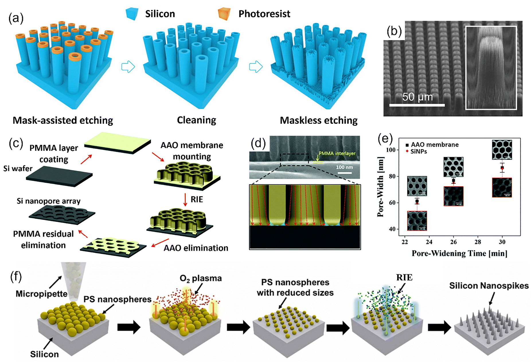 | ||
| Fig. 6 Mask utilization in RIE. (a) Schematic illustration of masked and maskless RIE. (b) SEM image of chimney-like arrays.65 Reproduced with permission from ref. 65. Copyright 2020, John Wiley & Sons. (c) AAO membrane transfer and mask etching process. (d) AAO membrane/PMMA/silicon substrate. The blue sections signify the PMMA sandwiched in the gaps. (e) Diameter variation of AAO nanopores and silicon nanopores at different pore-widening times; the inset SEM images show the corresponding AAO membrane and the etched silicon nanopores.98 Reproduced with permission from ref. 98. Copyright 2015, Royal Society of Chemistry. (f) Process of PS nanospheres for mask-RIE.28 Reproduced with permission from ref. 28. Copyright 2023, Elsevier. | ||
AAO masks are typically prepared through a two-step anodization process of high-purity aluminum foils.98,102–104 In the first anodization, aluminum is electrochemically oxidized in an acidic electrolyte such as oxalic, sulfuric, or phosphoric acid, leading to the formation of a porous alumina layer with a disordered arrangement. This layer is then chemically removed, leaving a textured aluminum surface. A second anodization under the same conditions produces a highly ordered hexagonal array of nanopores, whose diameter and interpore distance can be tuned by the choice of electrolyte, anodization voltage, and temperature. Subsequent pore-widening treatment in phosphoric acid allows further adjustment of pore size. The resulting AAO template can serve as a cost-effective, self-assembled nanomask for pattern transfer onto silicon during black silicon fabrication. Lin et al. transferred an AAO mask onto the surface of a silicon wafer spin-coated with a polymethyl methacrylate (PMMA) film.98 The PMMA interlayer eliminates gaps to make good contact between the AAO film and the wafer, also avoiding unneeded etching in the shielded area, achieving high-precision aperture control, as shown in Fig. 6(c)–(e). The diameters of silicon nanopores are very close to AAO nanopores.
For PS spheres, as depicted in Fig. 6(f),28 usually large-diameter PS spheres are self-assembled onto the wafer surface, and then ICP or RIE with O2 plasma is applied to shrink the diameter of the spheres and enlarge the inter-sphere spacing, which allows fine control over the mask geometry. After this step, the exposed regions of the wafer are etched with RIE, transferring the periodic arrangement of the PS spheres into ordered micro–nanostructures on the silicon surface. By tuning the initial sphere size, plasma treatment time, and etching parameters, the resulting structure size and periodicity can be flexibly adjusted. This bottom-up lithography approach is attractive due to its low cost and simplicity; however, issues such as sphere agglomeration, limited large-area uniformity, and difficulty in achieving defect-free ordering remain challenges for practical applications.
In addition to cryogenic RIE, black silicon can also be fabricated through the Bosch process, also known as deep reactive ion etching (DRIE), which alternates between etching and passivation steps to form high-aspect-ratio nanostructures.105 A typical cycle consists of three sequential steps: anisotropic etching of silicon by SF6 plasma, conformal deposition of a fluorocarbon passivation film by C4F8, and selective removal of the passivation layer at the trench bottom to enable vertical progression of the etch front. The iterative alternation of these steps suppresses lateral etching while maintaining verticality, compared with conventional RIE that often suffers from sidewall tapering and limited aspect ratios. As a result, aspect ratios exceeding 10:1 can be readily achieved, making the Bosch process indispensable for microelectromechanical systems (MEMSs),106 microfluidics, and nanostructured silicon fabrication.
By optimizing the balance between etching and passivation, the Bosch process can generate nano-jungle structures with very high aspect ratios on silicon.14 These nanostructured black silicon surfaces offered enhanced light trapping, improved wettability control, and superior mechanical robustness compared to conventional nanograss black silicon.
Furthermore, nanoparticle-assisted Bosch processes have been demonstrated to be an effective route for engineering needle-like silicon nanowires with dual functionalities, including broadband antireflection and superhydrophobicity.107 In this approach, PS nanospheres or other colloidal nanoparticles serve as a self-assembled etch mask, introducing local variations in the etching front. During the cyclic Bosch process, the presence of nanoparticles promotes the anisotropic evolution of high-aspect-ratio protrusions, resulting in dense silicon nanowire arrays with needle-like morphology. These structures integrate both optical and surface advantages: the elongated nanowires provide strong light scattering and multiple internal reflections to reduce reflectance, while their sharp, high-density features lower the solid–liquid contact area, thereby enhancing water repellency.
Hydrogen-containing plasmas, particularly CF4/H2 mixtures, have been demonstrated as an effective maskless route for black silicon fabrication. Vassallo et al. showed that by applying RF powers of 200–280 W for 20–30 min, well-defined nanostructures with lateral dimensions of 50–300 nm and depths of 100–300 nm were uniformly produced on silicon surfaces.108 These nanoscale pillars substantially suppressed reflectance to below 5% across the visible to near-infrared range. Importantly, the study introduced a hydrogen-based passivation mechanism, in which hydrogen replaces oxygen to form volatile HF while simultaneously promoting CFx passivation layer deposition. A related mechanistic study confirmed that in CF4/H2 plasma, fluorine radicals act as the primary etchants,109 whereas H2 serves both as a scavenger of fluorine and as a passivating agent, thereby enabling the self-organized formation of high-aspect-ratio nanostructures without lithographic masks. Together, these results highlight hydrogen plasma as a cost-effective and scalable alternative for black silicon fabrication with excellent optical performance.
RIE demonstrates broad applicability across various silicon wafer types and offers precise control over the etching process. Unlike other methods, RIE offers the advantage of fabricating black silicon not only on flat substrates but also on thin films and curved surfaces.66 When a highly curved hemispherical silicon lens was placed in the etching chamber, the electric field perpendicular to the surface bent, allowing ions to accelerate along the gradient and impinge on the sample surface nearly vertically. This process results in microstructures aligned parallel to the surface normal. However, the etching must occur in a vacuum chamber at low temperatures to minimize surface damage and prolong the carrier lifetime.97
2.3. Metal-assisted chemical etching
MACE is an advanced etching technique that evolved from conventional chemical etching, utilizing the catalytic properties of metal nanoparticles to achieve faster etching rates and greater control over surface structures.110 MACE preparation methods are typically categorized into one-step or two-step processes, based on how metal nanoparticles are introduced onto the silicon surface. In the one-step method, a mixed solution containing HF, HNO3 (or hydrogen peroxide (H2O2)), and silver nitrate (AgNO3) or chloroauric acid (HAuCl4) is used.110,111 In this process, metal nanoparticles are formed in situ on the silicon surface and simultaneously act as catalysts for localized etching. This method is simple and efficient, but the distribution and size of the nanoparticles are less controllable. In the two-step method, metal nanoparticles are first deposited onto the clean silicon wafer surface using techniques such as sputtering, evaporation, or solution reduction. The wafer is then immersed in an etchant solution (typically HF and an oxidant), where redox reactions at the metal-silicon interface induce anisotropic dissolution beneath the metal sites. Compared with the one-step method, this approach allows finer control over particle density, morphology, and etching uniformity, thereby enabling more reproducible nanostructure fabrication.Although the precise mechanism of MACE is not yet fully understood, it is widely accepted that localized redox reactions occur at the metal-silicon interface after nanoparticle deposition. These reactions selectively etch the silicon beneath the metal particles, creating highly controlled surface morphologies. The whole process is illustrated in Fig. 7. The etching mechanism of MACE in HF/H2O2 solution is represented by the equations listed in the left section of Table 2, including two half-reactions at the cathode and anode.38,112 In contrast, the reactions occurring in HF/HNO3 solution are shown in the right section.54,113 Key factors influencing MACE include the type and distribution of metal particles, etching time,12,114 crystal orientation, and composition of etchant.115
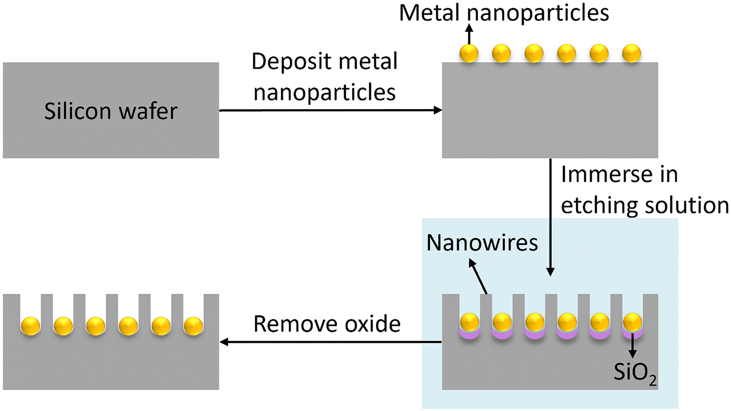 | ||
| Fig. 7 Fabrication mechanism of MACE. | ||
| Etching solution | HF + H2O238 | HF + HNO354,113 |
|---|---|---|
| Cathode | H2O2 + 2H+ + 2e− → 2H2O | HNO3 + 3H+ → NO + 2H2O + 3h+ |
| HNO3 → HNO2 → NO → HNO → H2N2O2 →N2O | ||
| Anode | Si + 2H2O + 4h+ → SiO2 + 4H+ | Si + 2H2O + nh+ → SiO2 + 4H+ + (4 − n)e− |
| SiO2 + 6HF → H2SiF6 + 2H2O | SiO2 + 6HF → H2SiF6 + 2H2O | |
| Si + 6F− + 2H+ + 2h+→ SiF62− + H2 | ||
| Overall |

|
Si + 6HF + NO3− → NOx + H2SiF6 + 2H2O |
| Note | • n = 2, silicon dissolves directly to form SiF62− | |
| • When the number of cavities at the Si/electrolyte or metal/electrolyte interface increases, dissolution occurs in the tetravalent system | • n is the average number of holes required to dissociate one Si atom | |
| • n = 2 in the divalent system, n = 4 in the tetravalent system, and n = 3 when both systems are present simultaneously | • HNO3 decomposes throughout the process | |
Table 3 provides a comparative overview of representative metal catalysts used in MACE, highlighting how differences in catalytic behavior translate into distinct etching regimes and morphology evolution pathways. Rather than ranking individual metals, the comparison emphasizes trade-offs among etching efficiency, structural controllability, and process robustness. Such a perspective is particularly relevant for tailoring black silicon architectures toward specific functional targets, where catalyst selection and post-deposition treatments collectively define the accessible parameter space for nanostructure engineering.
| Metal catalyst | Typical deposition method | Etching characteristics | Morphology control | Stability during etching | Representative features |
|---|---|---|---|---|---|
| Ag (one-step) | HF/AgNO3 mixed solution; Tollens’ reagent; chemical reduction | High etching rate; strong catalytic activity | Good directional control; favors nanowire and porous structures | Moderate; prone to dissolution and migration | Most widely used catalyst; high-aspect-ratio nanostructures; ordered Ag nanoparticle arrays via patterning |
| Ag (two-step) | Ag nanoparticle deposition + thermal annealing | Etching rate depends on nanoparticle shape and spacing | Strongly tunable via annealing temperature | Moderate | Annealing alters Ag nanoparticle geometry, significantly affecting reflectance behavior |
| Au | Thermal evaporation; sputtering; chemical deposition | Moderate etching rate; relatively uniform hole injection | High precision in etching location; pore-size controllable | High chemical stability | More stable than Ag; suitable for precise and localized etching, expensive |
| Pt | Physical or chemical deposition | Very high catalytic activity; fast etching | Enables ultra-high-aspect-ratio nanostructures | High | Higher etching rates than Au; excellent stability but limited by high cost |
| Pd | Physical or chemical deposition | High catalytic efficiency | Nanowires or nanoporous layers | High | Comparable etching rates to Pt; relatively expensive, limiting large-scale use |
| Ru | Thin-film deposition | Moderate etching rate | Pore-size control comparable to Au | High | CMOS-compatible catalyst; good stability with precise morphology control |
The crystallographic orientation of the substrate further governs the etching direction. In a study, the influence of p-Si (100) and (111) wafers on etching behavior in an acidic solution was analyzed,117 revealing significant differences in the resulting surface morphology. This finding suggests that wafer orientation impacts the etching process dynamics. Chen et al. further demonstrated that (100)-oriented silicon wafers exhibit a higher average etching rate in alkaline solutions compared to (110) and (111)-oriented wafers.86 Consequently, most black silicon studies focus on (100)-oriented wafers due to their superior etching characteristics. Kim et al. provided a microscopic electrochemical explanation for this dependence.37 During etching, H2O2 is rapidly consumed near the reaction front, establishing a steep concentration gradient that oscillates periodically due to diffusion-driven replenishment. These fluctuations modulate the etching directions: at low H2O2 concentration, etching proceeds preferentially along the vertical 〈100〉 orientation, whereas high concentrations promote etching along non-〈100〉 directions. Temperature also couples with this effect. At elevated temperatures, the accelerated decomposition of H2O2 generates more holes, rendering densely packed crystal planes with higher back-bond density, such as {111}, unstable against oxidation. Under such conditions, these planes are also etched, whereas under low H2O2 concentration, only the less back-bonded {100} planes are selectively attacked.
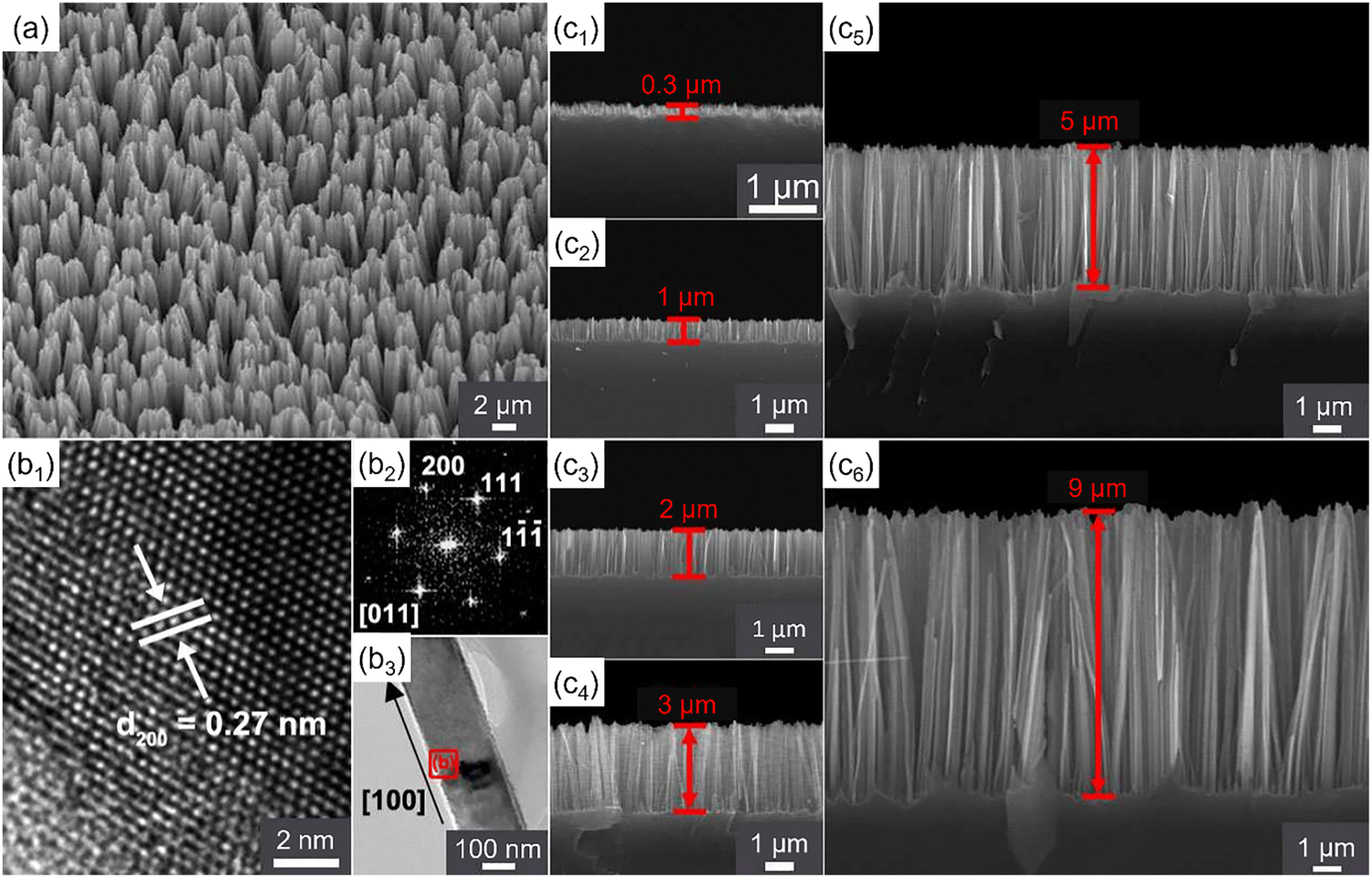 | ||
| Fig. 8 Images of SiNWs of different etching times.114 Reproduced with permission from ref. 114. Copyright 2010, Optica Publishing Group. (a) SEM image of the SiNW array formed on n-type (100) Si substrates. (b) TEM images of SiNWs with an average diameter of 150 nm. The lattice-resolved image and the corresponding FFT pattern confirm that the SiNWs are oriented along the [100] direction. (c) Side-view SEM images of SiNW arrays with different lengths of 0.3 µm, 1 µm, 2 µm, 3 µm, 5 µm, and 9 µm from (c1) to (c6), respectively. | ||
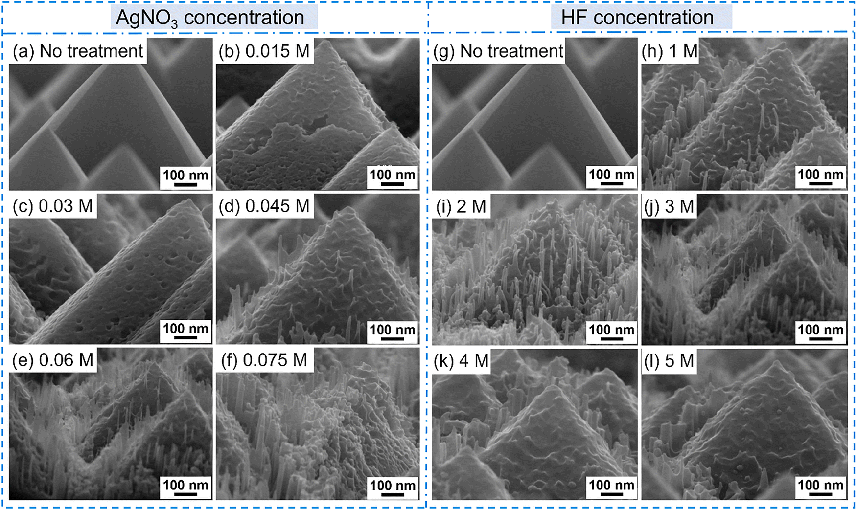 | ||
| Fig. 9 Influence of etchant composition on the formation of black silicon.125 Reproduced with permission from ref. 125. Copyright 2022, Springer Nature. (a)–(f) SEM images of samples etched in solutions with different AgNO3 concentrations. (g)–(l) SEM images of samples etched in solutions with different HF concentrations. | ||
HF solution generally exhibits a higher etching rate but offers limited controllability. Replacing HF with ammonium fluoride (NH4F) significantly slows down the reaction kinetics, thereby improving controllability and reducing pore formation in the etched structures.126 At the same molar concentration, the weight loss of silicon etched in HF solution is higher than that in NH4F solution (2.88 g vs. 2.78 g after 5 min), confirming the lower etching efficiency of NH4F. The resulting nanograss on textured silicon becomes denser and more vertically aligned, often presenting petal-like features at the pyramid tips due to the preferential vertical growth. Moreover, the reduced height of the nanostructures leads to a slightly lower effective refractive index compared with conventional HF-etched black silicon. It should be noted that NH4F is still a hazardous fluoride salt: although less percutaneously penetrating and systemically toxic than aqueous HF, it is corrosive and can release HF under acidic conditions. Therefore, appropriate protective equipment and fume-hood operation are essential when handling NH4F.
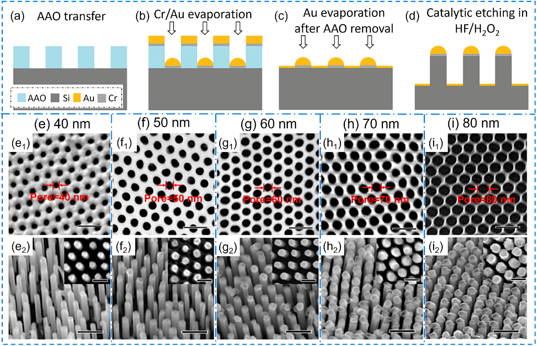 | ||
| Fig. 10 Schematic and SEM images of AAO template-assisted-MACE.70 Reproduced with permission from ref. 70. Copyright 2010, American Chemical Society. (a)–(d) Fabrication process of the AAO-template-assisted MACE. (e)–(i) SEM images of the AAO templates and the corresponding SiNWs with average diameters of 40, 50, 60, 70, and 80 nm, respectively. Insets show the top-view SEM images of the SiNWs. The scale bars are 200 nm in all SEM images and 100 nm for all the insets. | ||
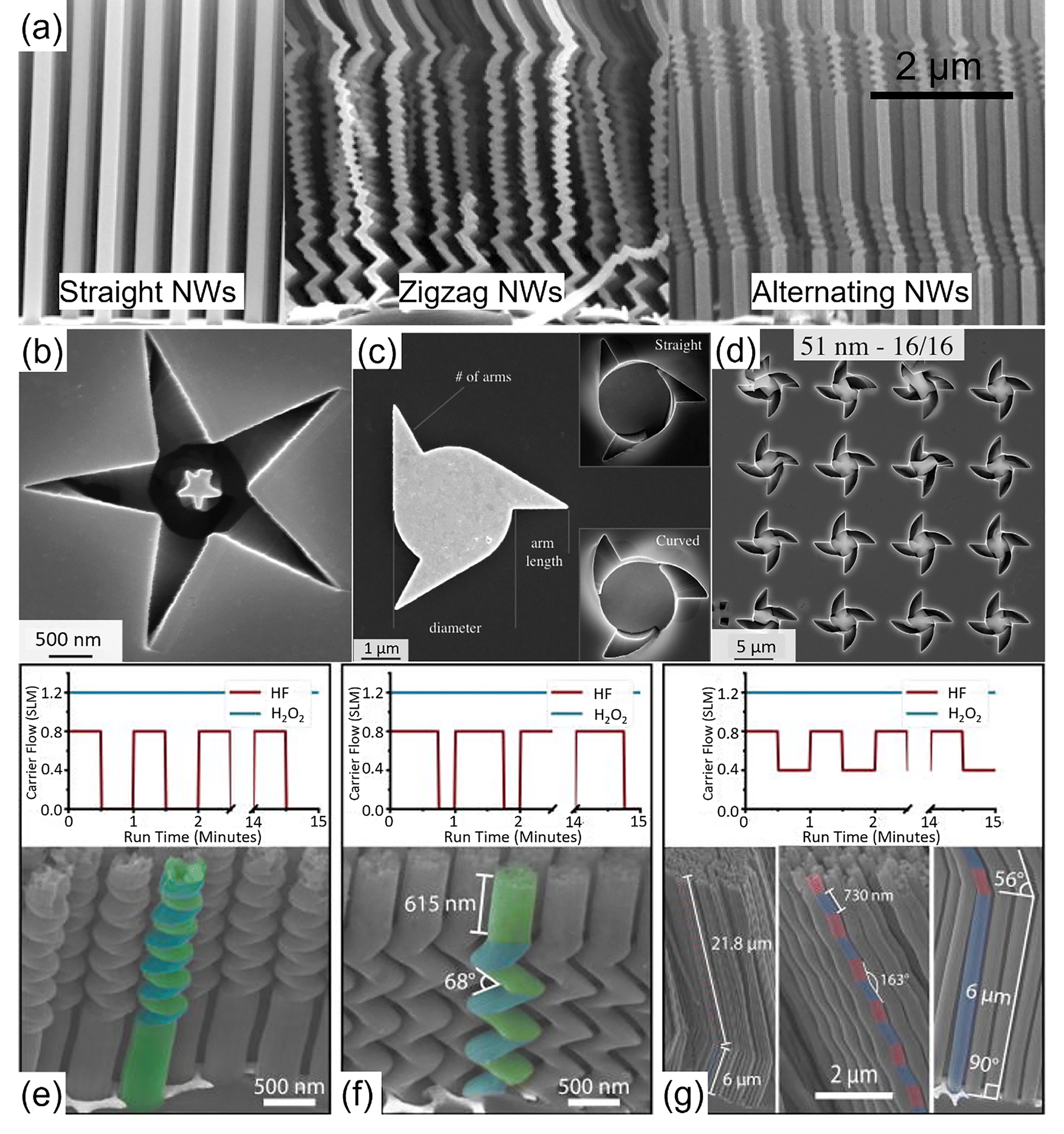 | ||
| Fig. 11 SEM images of representative nanostructures fabricated by direct MACE. (a) Nanowires with varying morphology obtained by tuning the etchant composition and etching time.131 Reproduced with permission from ref. 131. Copyright 2017, American Chemical Society. (b)–(d) Different 3D spiraling shapes fabricated via MACE.132 Reproduced with permission from ref. 132. Copyright 2012, American Chemical Society. (e) Periodically kinked nanowire arrays. (f) Zigzag nanowires. (g) H2O2 molar-ratio modulated nanowires.61 Reproduced with permission from ref. 61. Copyright 2023, AIP Publishing. | ||
Moreover, MACE facilitates the production of 3D nanostructures within a single etching cycle.132 The etched profile is influenced by the metal nanoparticles’ shape, and by tailoring the catalyst's geometry, diverse 3D structures can be achieved, such as spirals, as depicted in Fig. 11(b)–(d). Although this flexibility allows the fabrication of complex nanostructures, achieving structural uniformity and large-area scalability remains challenging due to manual control of etching parameters. To overcome these limitations, vapor-phase MACE (VP-MACE) has been developed.133 VP-MACE delivers HF/H2O2 vapors to the substrate surface, where they condense into a nanometer-thin liquid layer (<2 nm). Etching occurs only beneath the catalyst, yielding feature resolution comparable to liquid-phase MACE while eliminating bubble formation and preventing the generation of micro- and mesoporous silicon. Catalyst motion is governed solely by near-surface forces, enabling 3D trajectory control and the formation of helical nanostructures. VP-MACE thus improves uniformity, prevents stiction, and enhances resolution in silicon nanofabrication. Building on VP-MACE, programmable approaches introduce independent control over etchant flow rate, pulse time, chamber pressure, substrate temperature, and optional light illumination.61 By synchronously or asynchronously tuning these parameters, catalyst motion and etch profiles can be precisely engineered, enabling reproducible fabrication of nanowire arrays, point-etched structures, and complex 3D geometries, as illustrated in Fig. 11(e)–(g). This programmability enhances versatility, scalability, and process automation, making VP-MACE a powerful platform for high-aspect-ratio and multifunctional silicon nanostructures.
Another One-step MACE method was used to form nano/micro-hybrid structural arrays.134 Single-crystal Si substrates coated with catalytic metal films and photoresist were patterned via photolithography and ion-beam etching to pre-form micron-scale structures, and metal nanoparticles were deposited. After a solution reaction, small nanostructures were formed on the micron-scale structures. This method can also form nano/micro hybrid structure arrays of different shapes, such as circles, rectangles, and triangles, “pentagram”-shaped, and “peanut”-shaped.
In conclusion, MACE offers significant advantages over other nanofabrication methods, making it a highly promising technology for a wide range of applications. One of its key strengths is its broad applicability to various silicon surfaces, including monocrystalline silicon, polycrystalline silicon, and thin-film silicon, demonstrating its versatility across silicon substrates.69 MACE also stands out for its scalability, simplicity, and adaptability. It can be seamlessly integrated with other techniques, such as lithography and masking techniques, to achieve precise and directional preparation of surface morphologies. Additionally, its low cost and compatibility with existing manufacturing processes make it ideal for large-scale industrial applications, while offering both efficiency and cost-effectiveness. These advantages position MACE as a cutting-edge solution for fabricating advanced nanostructures across a wide range of industries.
2.4. Femtosecond and nanosecond laser etching
Laser irradiation enables the fabrication of black silicon by precisely ablating and doping silicon surfaces in a single step. This process is independent of the silicon grain orientation.135Fig. 12(a) shows a schematic diagram of this fabrication process.136 In this setup, cleaned silicon wafers were placed in a vacuum chamber, which is mounted on a 3D stage to control the laser's position along the XY plane, while the Z-axis adjusts the laser spot size focused on the wafer, thereby determining the laser fluence. A neutral density filter was used to ensure the laser fluence remains at optimal levels.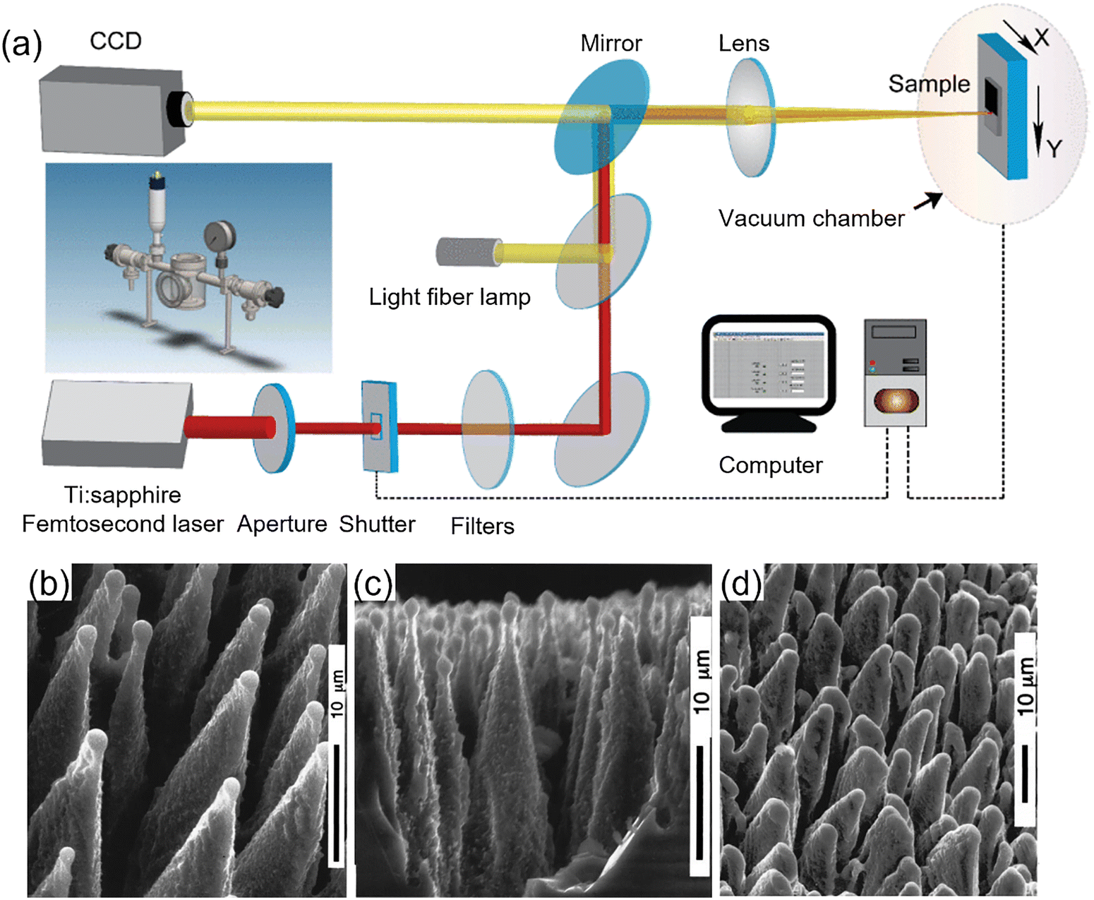 | ||
| Fig. 12 (a) Schematic of the femtosecond laser irradiation setup.136 Reproduced with permission from ref. 136. Copyright 2016, IEEE. (b) SEM image of sharp conical spikes oriented 45° from the surface normal. (c) SEM image of sharp conical spikes oriented parallel to the surface. (d) SEM image of the structures formed in vacuum.55 Reproduced with permission from ref. 55. Copyright 1998, AIP Publishing. | ||
In contrast to the smooth holes, trenches, and cavities created by femtosecond irradiation before,137 arrays of sharp conical spikes were also formed by irradiating silicon surfaces with 500 laser pulses of 100 fs duration and a fluence of 10 kJ m−2 in 500 Torr SF6, as first reported in 1998.55 As shown in Fig. 12(b) and (c), the conical spikes are always oriented in the direction of the incident light and independent of gravity, and the morphology in chlorine (Cl2) was consistent with SF6. The spherical caps implied that they originated from the dissolution of liquid silica droplets before the liquid wetted the spikes. However, it formed irregular blunt spikes in vacuum (Fig. 12(d)), N2 and helium (He) gas, indicating there were chemical reaction between SF6 or Cl2 to form sharp spikes.
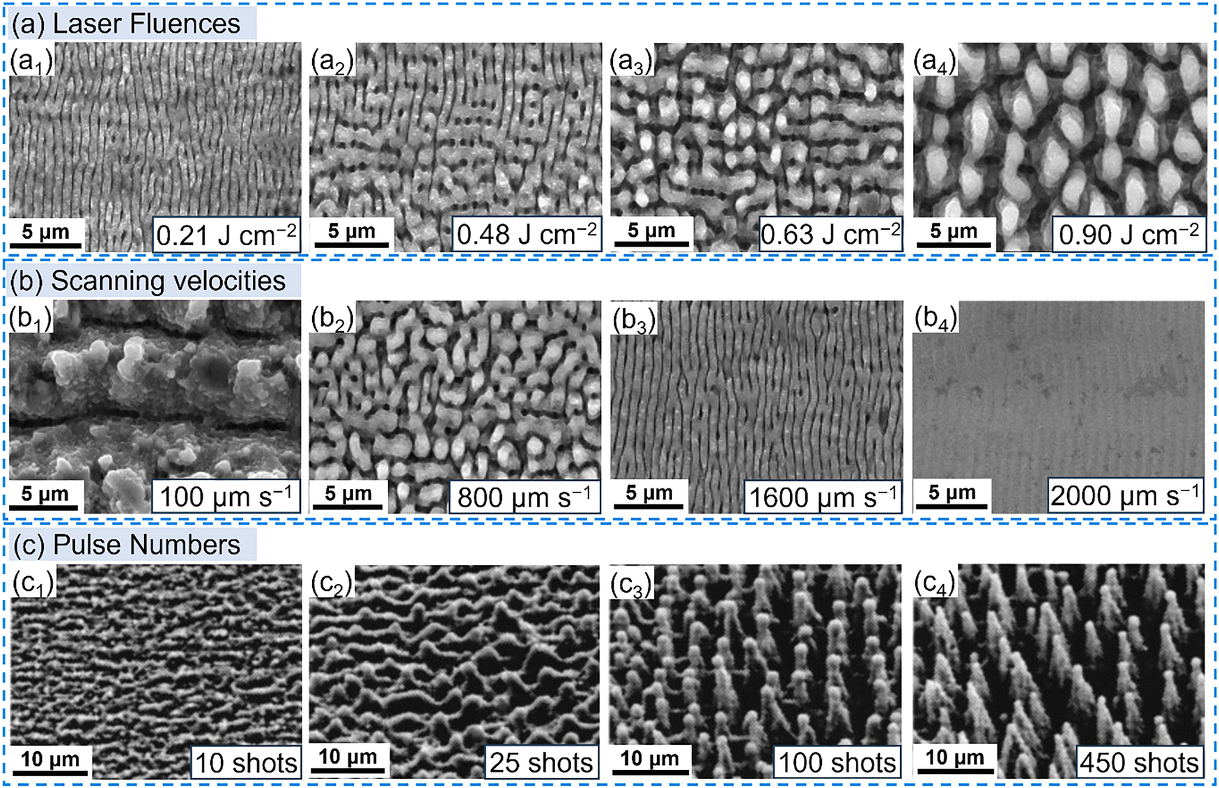
In femtosecond laser etching, ultrashort pulses create localized, high-temperature plasma on the silicon surface, inducing rapid melting, vaporization, and resolidification, which collectively lead to the formation of nanostructures such as spikes or pores.138 This process minimizes heat diffusion, ensuring precise material modification and reducing thermal damage. In contrast, nanosecond laser etching involves longer pulses that generate broader heat-affected zones,139 leading to micro- and nanostructure formation through thermal ablation, melt expulsion, and capillary instabilities. Nanosecond laser irradiation tends to produce smoother surfaces due to longer melting times and slower rates, while femtosecond laser irradiation results in sharper, more distinct features. Typically, structures formed by femtosecond lasers are about 8 µm in height with ∼4 µm spacing, whereas structures formed by nanosecond lasers can reach ∼40 µm in height and are spaced ∼2 µm apart. Representative morphologies produced by femtosecond laser irradiation (Fig. 13(a) and (c)) and nanosecond laser irradiation (Fig. 13(b) and (d)) are shown in Fig. 13.140
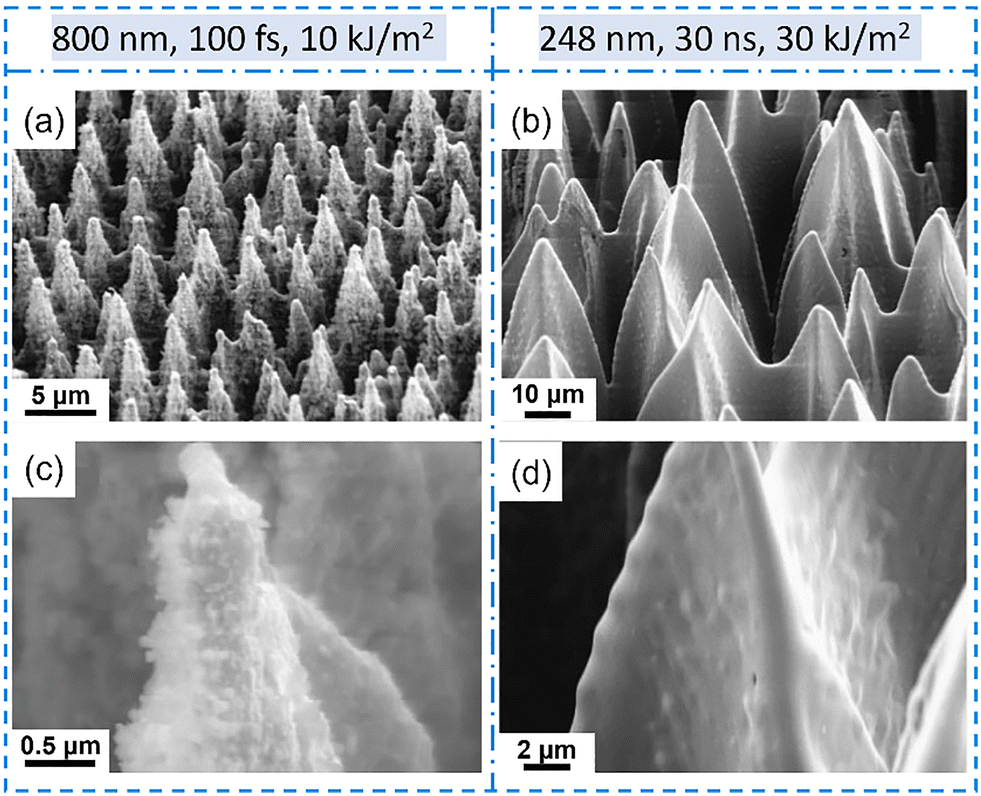 | ||
| Fig. 13 SEM images of structures produced by femtosecond and nanosecond laser irradiation.140 Reproduced with permission from ref. 140. Copyright 2004, AIP Publishing. (a) Morphology generated by femtosecond laser irradiation with a laser wavelength of 800 nm, a pulse duration of 100 fs, and a fluence of 10 kJ m−2. (b) Morphology produced by nanosecond laser irradiation with a laser wavelength of 248 nm, a pulse duration of 30 ns, and a fluence of 30 kJ m−2. (c) Enlarged SEM image corresponding to (a). (d) Enlarged SEM image corresponding to (b). | ||
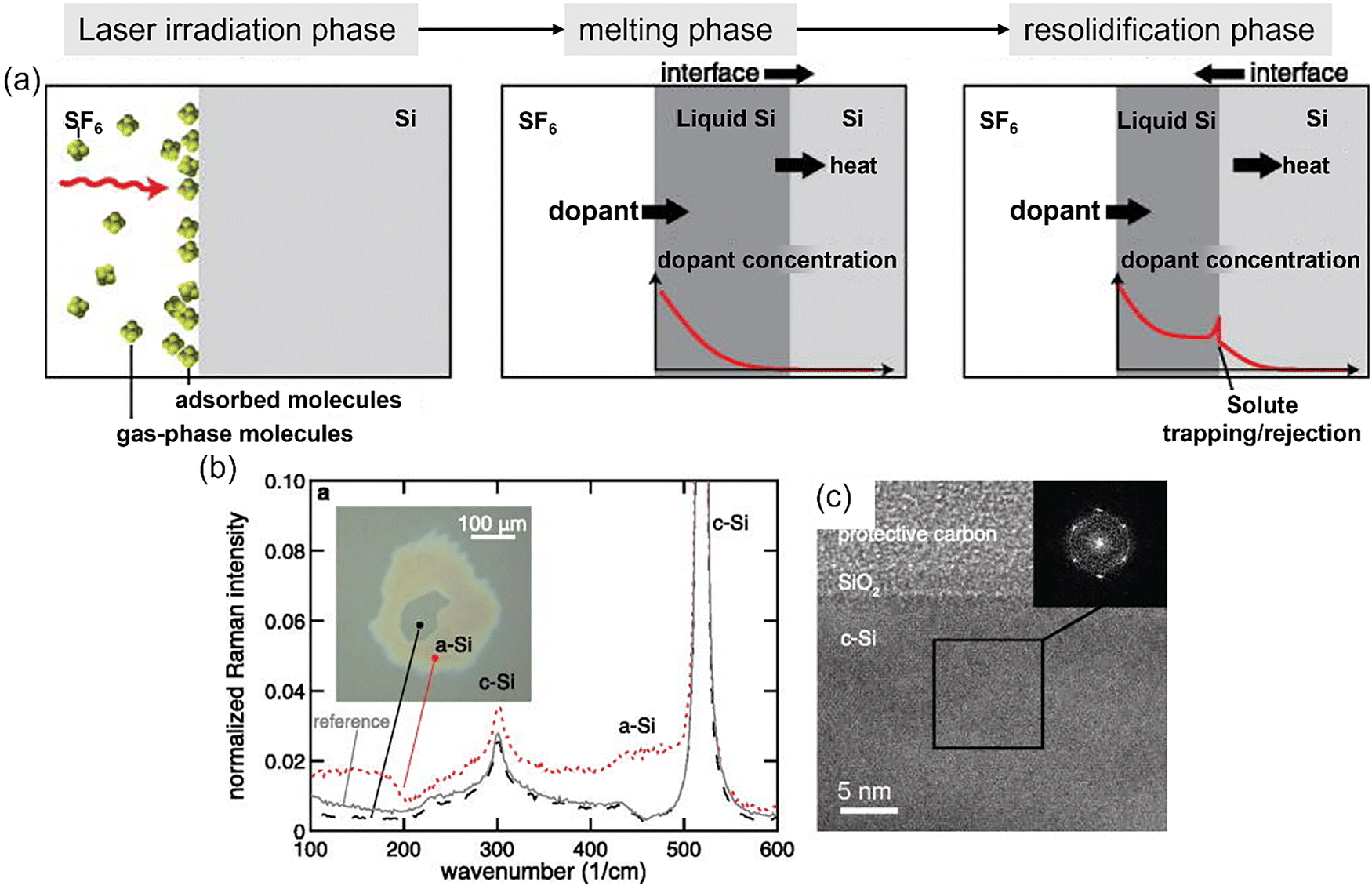 | ||
| Fig. 14 Melting and doping processes during laser etching.141 Reproduced with permission from ref. 141. Copyright 2015, AIP Publishing. (a) Illustration of the doping process during silicon melting. (b) Normalized Raman intensity curves of molten silicon. The inset shows the corresponding optical microscope image. (c) Bright-field TEM image of the laser irradiation center. The inset shows the corresponding FFT pattern. | ||
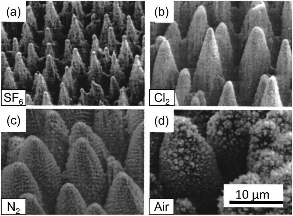 | ||
| Fig. 15 SEM images of black silicon in different ambient gases.72 Reproduced with permission from ref. 72. Copyright 2003, AIP Publishing. (a) SF6. (b) Cl2. (c) N2. (d) Air. | ||
The presence of sulfur promotes the formation of sharp conical spikes; as sulfur concentration in the environment increases, the tip area of each microstructure decreases. Pre-coating the silicon wafer with the doping layer has been shown to further reduce reflectivity in ambient air.142 When coated silicon is ablated by the laser, impurity atoms on the surface are trapped in the molten state and doped during the formation of micro- and nanostructures.
In conclusion, femtosecond laser irradiation presents a powerful technique for black silicon fabrication, offering key advantages such as efficient doping, broadened absorption spectra, and precise control of surface morphology. However, challenges remain, including high production costs, potential environmental concerns during fabrication, and lengthy processing times.
2.5. Plasma immersion ion implantation etching
Ion implantation is a surface modification technique where ions are injected into a solid material to alter the physical and chemical properties of its surface without affecting its bulk characteristics. However, the doping concentration declines rapidly with increasing depth in the sample.147 Plasma immersion ion implantation is often used for semiconductor doping. The principle was summarized by Cheung in 1996.57 Xia et al. first used this method to produce needle-like structures on the silicon surface in 2011,22 and the forming mechanism is represented in Fig. 17(a).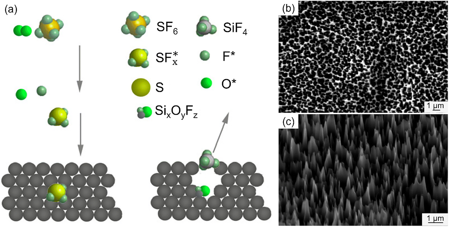 | ||
| Fig. 17 Mechanism and SEM images of PIIIE-fabricated black silicon.22 Reproduced with permission from ref. 22. Copyright 2011, Elsevier. (a) Mechanism of the PIIIE process. (b) SEM image of the black silicon surface (top view). (c) SEM image of the black silicon surface (side view, viewed at 30° to the surface normal). | ||
In this process, plasma was generated at 900 W radio frequency power. SF6 plasma gas provided the F+, SF+, SF3+, and SF5+ ions, and O2 plasma generates O* radicals. With –500 V pulses applied to the sample stage, the SFx+ (x ≤ 5) and F+ were injected into the silicon substrate. These reactive ions reacted with silicon and formed a uniform microstructure on the silicon surface after the volatile SiF4 was formed and escaped. After that, the O* radicals reacted with the fresh surface rapidly to form SiOx. The SiOx layer then interacted with the SFx+ (x ≤ 5) and F+ ions to produce the SixOyFz, which partially escaped under the effect of ion bombardment and were further etched by the SFx+ (x ≤ 5) and F+ ions. Finally, the porous or needle-like microstructures of black silicon were formed (Fig. 17(b) and (c)). This process reduced the reflectance to 1.79%, significantly lower than 12.07% for textured silicon (NaOH/IPA etching) and 30.01% for polished silicon.
The PIIIE process is a gas-phase etching technique; the key influencing factors include gas composition, RF power, bias voltage, gas flow rate, etching time, pressure, and temperature.
The influence of the SF6/O2 gas flow ratio was studied by Xia et al.,80 as shown in Fig. 18(a). With an increasing SF6/O2 ratio (Fig. 18(a2)–(a4)), the surface morphology of black silicon changed from a porous structure to a needle structure, and the reflectivity decreased sharply. However, when only SF6 was used as the plasma gas (Fig. 18(a1)), the O and F concentrations on the surface were very low, and the surface could only become rough with high surface reflectivity.
 | ||
| Fig. 18 SEM images of black silicon prepared by PIIIE under different processing parameters. (a) Composition of reactive gases.80 Reproduced with permission from ref. 80. Copyright 2012, Elsevier. (b) Bias voltage. (c) H2 flow rate.82 Reproduced with permission from ref. 82. Copyright 2018, Elsevier. | ||
In Lim's research,82 H2 and Ar feedstocks were used in the plasma etching process, with RF power and bias voltage serving as crucial factors in converting neutral gases into reactive species. The influence of bias voltage is illustrated in Fig. 18(b). At a low bias of −25 V, large and random nanohumps and clusters form. Increasing the bias to −50 V reduces the cluster size, filling them with smaller or larger nanohumps. At −75 V, high-density and well-arranged nanocones emerge, whereas further increasing the bias to −100 V causes the nanocones to break, resulting in thin and fragmented nanobranches. A low bias voltage produces a weak sputtering effect, leading to agglomeration of sputtered atoms, while a higher bias promotes the formation of sharp, well-defined cones.
In addition, the influence of H2 flow was investigated. Increasing the H2 flow leads to the discharge quenching and reduces the density of active substance in the plasma etching process, thus affecting the surface structure. A denser discharge can be obtained at higher RF power. As shown in Fig. 18(c), as H2 flow increases, the structure evolves from dense and sharp nanograss tips to wider nanocones and eventually pyramid-like structures, with increasing nanostructure size and decreasing density. The reflectivity of the samples decreased gradually in this process, implying that, in addition to an appropriate aspect ratio, the nanostructure density also has an effect on the reflectance of light.
PIIIE is an advanced method for fabricating black silicon, offering high controllability and doping capability. However, ion implantation concentration diminishes rapidly with depth, and the need for expensive equipment limits its wider application.
2.6. Comparative insights: process-structure-state correlations
The morphology of black silicon differs significantly due to the distinct mechanisms involved in materials removal and structure formation. Chemical etching techniques, including acidic chemical etching, electrochemical etching, and molten salts electrochemical etching, typically result in isotropic structures, while alkaline chemical etching leads to anisotropic structures due to its crystal-plane-selective etching behavior. Pure chemical etching produces irregular pits or porous morphologies, while electrochemical methods provide greater control, forming uniform pores or porous layers with tunable dimensions. Molten salts electrochemical etching, on the other hand, enables deeper and more defined porous structures but requires elevated temperatures and specific chemical environments. RIE forms well-aligned micro- and nanoscale structures, such as needle- or cone-like surfaces, through plasma-induced anisotropic etching, offering precise control over morphology but at the expense of higher equipment complexity and cost. MACE produces highly controlled vertical structures, such as nanowires or nanopores, by leveraging catalytic reactions at the metal-silicon interface. This method is cost-effective and compatible with large-scale production. Femtosecond and nanosecond laser etching methods create a wide variety of morphologies, from nanoripples to needle-like or hierarchical structures, by adjusting laser parameters such as fluence and pulse duration. Femtosecond lasers offer exceptional precision with minimal thermal damage, while nanosecond lasers are more accessible but lead to broader heat-affected zones. Finally, PIIIE combines plasma etching and doping, enabling the formation of needle-like or cone-shaped structures with controllable doping levels (∼1014–1018 ions cm−2).148 However, the process is limited to sub-micrometer depths due to the restricted ion energy and mean free path, and its relatively high cost further constrains large-scale applications.Each method offers distinct advantages tailored to specific applications, with trade-offs in cost, scalability, and structural control. For example, Tan et al. investigated the difference between the dry etching method (ICP-RIE) and the wet etching method (Ag-MACE), and found that wet etching produces longer nanostructures, but the morphology is less organized.150 For wet etching, the surface structure of black silicon can minimize the reflectivity within 300–1100 nm. Moreover, the needle tip part has better light absorption than the pit part, while the absorption efficiency of dry-tip (95%) is about 2% lower than that of wet-tip (97%), and the influence of needle tip and pit structure is not large in dry etching. More regular patterns often require lithography, while laser etching does not require an etching mask. RIE can form black silicon with high alignment and pattern transfer accuracy without affecting optical and electrical properties.149 The edge roughness of MACE patterns is often higher than that produced by RIE, and there is a noticeable contrast gradient near the edges, which may indicate uneven etching contours. The solutions used in the MACE process, such as HF and HNO3, limit the choice of photoresist. The differences among chemical etching, RIE, MACE, femtosecond and nanosecond laser irradiation, and PIIIE are summarized in Table 4.
| Method | Reaction condition | Main influencing factors | Morphology | |
|---|---|---|---|---|
| Chemical etching | Pure chemical etching | Acidic solution: HF + HNO3 | 1. Types of silicon | Acid solution: isotropic, porous |
| 2. Solution composition and concentration | Alkaline: anisotropic, pyramid | |||
| 3. Temperature | Higher HF: porous | |||
| Alkaline solution: NaOH/KOH+IPA | 4. Etching time | Higher HNO3: polish and remove damage | ||
| Electrochemical etching | HF solution | 1. Type and concentration of doping atoms | Mainly cones | |
| 2. Solution | Higher potential and HF concentration: polish silicon | |||
| 3. Potential | ||||
| Molten salts electrochemical | Molten salt solution | 1. Oxygen diffusion in the solid phase | Columns | |
| 2. Charge transfer | ||||
| 3. O2− diffusion in liquid phase | ||||
| RIE | ICP or CCP system with SF6/O2 plasmas | 1. RF and ICP power | Higher power: taller structure within limits | |
| 2. Etching time | Longer time: increase the width and depth of pores | |||
| 3. Gas composition | Higher SF6: shallow nanopores on side walls | |||
| 4. Pressure | Higher pressure: gentle surface | |||
| 5. Substrate temperature | Higher temperature: uniform and dense conical | |||
| 6. Bias voltage | Little effect after microstructure formation | |||
| 7. Mask | Desired nanostructures (penguin-like, hollow cylinders, etc.) | |||
| MACE | 1. Deposit nanoparticles | 1. Types of metal particles | Different catalytic activity and stability | |
| 2. Etching time | Longer time: higher height | |||
| 3. Composition of etchant | Higher AgNO3 and HF: from forming nanowires to excessively etched | |||
| 2. Reaction: HF + H2O2/HNO3, take H2O2 as example | 4. Types and orientation of silicon | Form different junctions and (100) orientation better | ||
| 5. Temperature | Higher temperature: stronger reactivity | |||
| 6. Mask | Desired nanowires (zigzag, spiraling shapes, etc.) | |||
| Fs and ns laser irradiation | Femtosecond laser and vacuum chamber with reaction gas | 1. Femtosecond or nanosecond laser | Femtosecond: sharp conical spikes | |
| nanosecond: smoother | ||||
| 2. Gas composition | Corrosive gas: sharp conical spikes | |||
| Inert gas: blunter structure | ||||
| 3. Parameters of laser (fluence, scanning velocity, pulse number) | Higher fluence, pulse number, and lower scanning speed: nanoripples to nanopores to sharp conical spikes | |||
| 4. Temperature | Help the silicon ablation | |||
| PIIIE | Vacuum chamber with reaction gas, most SF6 and O2 | 1. Gas composition | SF6/O2 ratio increase: porous to needle structure | |
| 2. Bias voltage and RF power | Voltage/power increase: nanohumps and clusters to nanocones to nanobranches | |||
| 3. Gas flow rate | Rate increase: bigger nanostructure size and lower density | |||
3. Micro–nano surface architectures of black silicon
The surface architecture of black silicon is a critical determinant of its multifunctional capabilities, influencing light absorption, charge carrier behavior, and interfacial properties. This section systematically reviews the interplay between morphological features and surface chemical states in shaping device performance. It first classifies the structural diversity introduced through micro- and nanoscale manufacturing technologies, highlighting how various morphologies (such as spikes, pores, and trenches) contribute to application-specific enhancements in light trapping, charge transport, and surface reactivity. Subsequently, it discusses the surface states and chemical terminations (e.g., Si–H, Si–O, Si–F) introduced during processing, emphasizing their influence on recombination behavior and doping. Finally, recent advances in surface passivation techniques are examined, with a focus on their effectiveness in enhancing the stability and functional efficiency of black silicon across optoelectronic applications.3.1. Structural diversity of surfaces
Black silicon refers to silicon surfaces that have been engineered to exhibit extremely high light absorption, typically resulting in a distinctive dark appearance. The morphology—meaning the specific shape, structure, and texture of the silicon surface—is instrumental in defining how black silicon interacts with light, heat, and other external factors. Different preparation techniques yield varied morphologies,77,151 each imparting distinct properties that are advantageous for specific applications such as photovoltaics, optoelectronics, sensors, and biomedical devices. There are several morphologies of black silicon (as shown in Fig. 19), each with distinctive characteristics.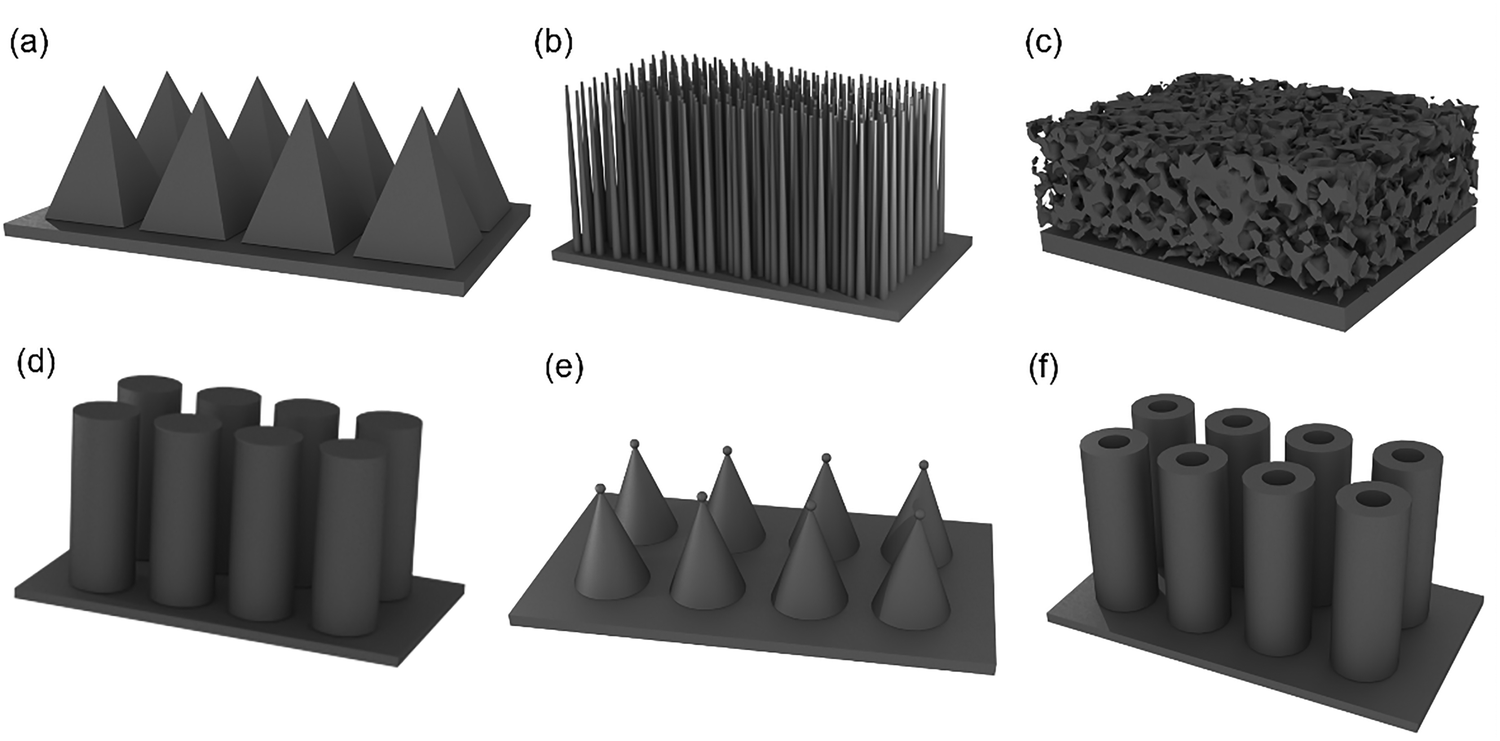 | ||
| Fig. 19 Different morphologies of black silicon. (a) Pyramid. (b) Nanowires. (c) Porous. (d) Columns. (e) Conical spikes. (f) Chimney-like array. | ||
Pyramid structures,152 as shown in Fig. 19(a), are commonly used in the solar cell industry as “textured surfaces” to maximize light absorption and thus increase photovoltaic conversion efficiency. These pyramids are influenced by their aspect ratio and grain orientation, which play a role in the reaction dynamics during formation.
Another morphology is silicon nanowires, as shown in Fig. 19(b),153 which are appreciated in semiconductor processing due to their high specific surface area. Their diameter and length can be precisely controlled to meet specific functional requirements, making them adaptable for a wide variety of applications, from sensing to energy storage. Recent advancements in fabrication have allowed even finer control over SiNWs' dimensions, resulting in intricate structures with enhanced electrical and optical properties. SiNWs are often produced through methods such as chemical vapor deposition or metal-assisted etching, where factors like catalyst size and etching time dictate the wire dimensions, enabling a high degree of customization.
Porous silicon is characterized by a highly irregular surface texture composed of interconnected pores,154 the morphology is shown in Fig. 19(c). The pore sizes typically range from nanometers to micrometers. This morphology is typically formed through electrochemical or chemical etching processes that dissolve parts of the silicon structure, creating a network of voids. The high porosity of this morphology results in an extensive surface area that is especially advantageous in applications requiring high reactivity or rapid diffusion, such as in sensors, photocatalysis, and supercapacitors. Additionally, porous silicon is a good candidate for drug delivery applications due to its capacity to carry and release molecules in a controlled manner, owing to the tunable size and distribution of its pores.
Columns (Fig. 19(d))155 often formed when a mask is used. Their high aspect ratio simultaneously enhances optical absorption and preserves desirable photoelectric properties, making them highly promising for optoelectronic applications.
Another distinctive morphology found in black silicon is that of sharp conical spikes (Fig. 19(e)).156 This structure is typically formed by irradiating the silicon surface with lasers in the presence of reactive gases, such as SF6/O2. In this process, high laser-induced temperatures promote chemical reactions that incorporate sulfur dopants into the silicon, resulting in hyperdoping and the formation of sub-bandgap states that extend optical absorption into the infrared. Moreover, the formation of sharp conical spikes significantly enhances light trapping and suppresses surface reflectance. The combined effects of sulfur hyperdoping and conical microstructure make this architecture highly promising for broadband optoelectronic applications.
Similarly, needle-like structures or “nanograss” result from plasma-based processes where high-energy ions create a densely textured surface with vertical needle features.14,157 This morphology offers versatile applications, including energy harvesting, self-cleaning materials, sensors, and biomedical devices.
When the micro- or nanostructures are precisely controlled through mask, lithography, or other patterning techniques, more precisely fabricated morphologies can be obtained,158–160 such as the chimney in Fig. 19(f). The light absorption can be enhanced further, and the specific morphology could achieve additional novel functionalities.
Each morphology offers unique advantages and can be customized through specific fabrication techniques, influencing the performance of black silicon in diverse applications. The selection of morphology and the tuning of its characteristics, such as size, aspect ratio, and orientation, are essential considerations in the design of high-performance silicon-based devices.
3.2. Surface states induced by micro–nano engineering
Beyond geometric morphology, the surface states introduced during micro–nano engineering play a pivotal role in shaping the optical and electronic behavior of black silicon. Processes such as anisotropic etching, plasma treatment, and chemical modification inevitably generate a variety of surface states, including structural defects, chemical terminations, and interfacial bonding irregularities. These states not only govern carrier trapping and recombination but also affect charge accumulation, band alignment, and long-term device reliability. This section explores the origins and functional impact of such surface states, focusing on defect-mediated carrier dynamics, the role of Si–H, Si–O, and Si–F terminations, and strategies for surface passivation. Understanding and controlling these factors is essential for optimizing black silicon performance across photovoltaic, sensing, and photodetection applications.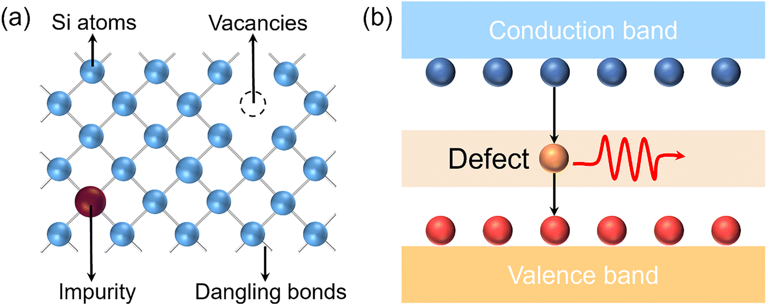 | ||
| Fig. 20 Defects and SRH recombination in silicon. (a) Dangling bonds, impurity, and vacancies in silicon. (b) SRH recombination. | ||
Carrier trapping and recombination via defect states. Surface and subsurface defect states, such as dangling bonds and dislocations, introduce localized energy levels within the silicon bandgap that act as non-radiative recombination centers.163,164 These trap states capture photo-generated carriers and facilitate indirect recombination through phonon interactions, leading to significant losses in carrier lifetime and diffusion length. This effect is particularly detrimental in optoelectronic devices such as photodetectors and solar cells, where efficient charge collection is critical under low-light intensity conditions.165,166
At the atomic scale, surface defects in black silicon primarily arise from the abrupt termination of the silicon lattice, resulting in unsatisfied valence electrons known as dangling bonds.167 Dangling bonds exhibit high reactivity and electronic trap properties due to their inability to form sufficient bonds with other atoms. These defects introduce localized energy levels within the bandgap, acting as recombination centers that capture carriers. The density of such bonds can reach ∼1015 cm−2.168 Even under ultra-high vacuum (10−10 Torr), silicon surfaces rapidly adsorb ambient species such as oxygen, forming a native SiO2 layer that passivates most of the dangling bonds.169 However, due to the lattice mismatch between silicon and SiO2, some interface states persist, enabling carrier exchange with the bulk and promoting Shockley-Read-Hall (SRH) recombination. The mechanism is shown in Fig. 20(b),170 when free charge carriers encounter defect levels, non-radiative recombination occurs and energy is released. Furthermore, fabrication processes including high-temperature treatment, ion implantation, and irradiation can introduce additional defect states that enhance carrier trapping and recombination. Lattice mismatch between silicon and SiO2 leaves some bonds unsaturated, allowing charge exchange with the bulk. Additional surface states can also result from fabrication-induced damage, such as high temperatures, ion implantation, or irradiation (e.g., X-rays, UV lasers).171
Therefore, controlling the density and nature of surface defect states is essential for minimizing recombination losses and enhancing the performance of silicon-based electronic and optoelectronic devices. A stable, low-defect surface is a prerequisite for achieving high sensitivity, low dark current, and strong photoresponse in advanced device architectures.
Defect-induced modulation of band structure and electric fields. In addition to serving as recombination centers, surface and interface defect states can significantly modulate the band structure and electric field distribution in semiconductor devices. These defects often act as charged centers by capturing carriers, forming fixed charge layers near the surface. Electron-trapping states typically lead to the accumulation of negative charges on the order of 1012 cm−2,172–175 while hole-trapping states may contribute to positive fixed charges.176,177 The spatial distribution and density of these charges influence the surface potential, induce band bending, and affect the width of space charge regions such as depletion layers in p–n junctions or Schottky interfaces.
The modulation of band bending caused by defect-induced fixed charges directly impacts the built-in electric field, which governs carrier drift and separation dynamics.178,179 Dangling bonds acting as charge traps increase carrier capture and recombination, contributing to leakage current and threshold voltage fluctuations in MOS devices. Over time, the accumulation of these defects can degrade device stability and lifetime. When the defect-induced electric field aligns with the internal field, it can aid charge extraction and improve performance. In contrast, an opposing field reduces charge collection, causes response hysteresis,180 saturation drifts, and threshold voltage shifts—particularly critical in low-light or high-speed optoelectronic applications.
While these phenomena are generally viewed as parasitic, they can also be intentionally exploited in certain device designs. In MOSFETs or thin-film transistors, for instance, surface states and interface dipoles can be engineered to adjust threshold voltages or modulate channel conduction.181,182 Nonetheless, in high-sensitivity detectors and high-speed photonic devices, the presence of such electrically active states is detrimental. Consequently, surface passivation strategies—such as thermal oxidation, ALD of high-k dielectrics, or self-assembled monolayers—are commonly employed to minimize trap densities and stabilize electrostatic conditions. Ultimately, understanding and managing the electrostatic influence of surface and interface traps is essential for optimizing both the static and dynamic performance of modern semiconductor devices.
Defect-enhanced surface reactivity. Beyond their electronic implications, surface defect states significantly enhance the chemical reactivity of silicon surfaces by acting as highly active adsorption and reaction sites.183–186 Defects such as dangling bonds, vacancies, and low-coordination atoms create localized electronic states with elevated local density of states, which facilitate stronger interactions with gas molecules and functional chemical species. These unsaturated sites exhibit high surface energy and chemical potential, making them preferential sites for adsorption via chemisorption or charge-transfer interactions.
In gas sensing applications, this defect-induced reactivity plays a pivotal role in determining both sensitivity and selectivity. In nanostructured black silicon, for instance, the combination of high surface area and abundant defects synergistically enhances gas-molecule adsorption and electronic modulation.25,26,187–189 Electron-acceptor molecules such as O2 and NO2 preferentially adsorb at these defect sites, leading to local charge transfer and the formation of ionized species. As shown in Fig. 21(a) and (b), in ambient air, O2 molecules adsorb on the surface of p-type black silicon, capturing electrons and forming negatively charged species. These species induce upward band bending and increase the surface depletion region. Upon exposure to NO2 (Fig. 21(c) and (d)), these adsorbed oxygen species undergo further reactions with NO2 molecules, extracting additional electrons and intensifying hole accumulation in the surface region. This results in a further increase in hole conductivity and a more pronounced change in the electrical response of the device. The adsorption process modifies the surface potential and band structure, often resulting in measurable changes in conductivity or surface barrier height. A higher density of active defect sites leads to more pronounced electrical signal changes upon exposure to analytes. This enhancement improves the response magnitude and lowers the detection limit (down to 1 ppm) while maintaining a rapid response time of approximately 12–14 seconds.
 | ||
| Fig. 21 Sensing mechanism of black silicon gas sensors for air and NO2.26 Reproduced with permission from ref. 26. Copyright 2025, Royal Society of Chemistry. (a) and (b) Air. (c) and (d) NO2. | ||
Similarly, in biosensing applications, surface defects facilitate the immobilization of functional biomolecules such as antibodies, aptamers, or enzyme-linked probes.190–193 These molecules tend to anchor more effectively at high-energy defect sites due to favorable binding affinity, allowing for stable and dense functional layer formation. This not only enhances target capture efficiency but also improves signal transduction, as biomolecular interactions near electronically active defects can induce local charge redistribution, further amplifying the output signal.
From a materials engineering perspective, the ability to modulate surface defect density provides a means of tuning reactivity for application-specific needs. Techniques such as plasma treatment, laser-induced surface reconstruction, and controlled chemical etching can be used to tailor the distribution and density of active sites. However, the enhancement in surface reactivity must be balanced against potential drawbacks such as increased carrier recombination. Therefore, rational defect engineering is crucial for optimizing multifunctional interfaces in silicon-based sensors and bioelectronic platforms.
Challenges and prospects in defect state control. While a moderate density of surface defect states can enhance chemical reactivity and functionalization capabilities, excessive defects often compromise electronic performance by increasing carrier recombination and instability. This inherent trade-off presents a core challenge in the functional tuning of micro- and nanostructured silicon: achieving an optimal balance between surface reactivity and electronic quality. To address this, various strategies have been explored to precisely control the type, distribution, and energy levels of defect states. For example, fine-tuning etching parameters,94,194–196 such as etchant concentration, temperature, and reaction time—can mitigate undesired lattice damage during structuring. Post-fabrication treatments such as ALD of dielectric coatings or surface reconstruction are effective in passivating dangling bonds and smoothing out surface disorder,197,198 thereby reducing non-radiative recombination while retaining sufficient active sites for surface interactions.
Despite these advances, achieving defect control at the atomic scale remains technically demanding, particularly for large-area and complex three-dimensional architectures. Moreover, the long-term stability of passivated states under environmental exposure poses additional reliability concerns for real-world applications.
| Chemical bonds | Si–H | Si–O | Si–F |
|---|---|---|---|
| Origin | Hydrogen plasma treatment, HF etching | Thermal oxidation, ALD, PECVD | Dry etching (e.g., SF6, CF4 plasmas) |
| Passivation mechanism | Chemical passivation (saturation of dangling bonds) | Chemical + field-effect passivation | Hydrophobic termination, weak chemical passivation |
| Passivation performance | Good | Good, enhanced by hydrogen | Poor |
| Thermal stability | Moderate | Excellent | High |
| Chemical stability | Moderate | High | Very high |
| Surface wettability | Neutral/hydrophobic | Hydrophilic | Hydrophobic |
| Interface defect control | Good | Moderate (requires additional treatment) | Poor |
| Post-treatment compatibility | Good (suitable for further functionalization) | Moderate (requires careful processing) | Poor (inhibits further modification) |
Surface terminations and their functional roles. Surface terminations play a vital role in determining the interfacial electronic behavior and chemical stability of micro- and nanostructured silicon.
Si–H terminations are typically formed after HF treatments or wet chemical etching processes.200–202 These terminations are highly effective at passivating surface dangling bonds by saturating unpaired electrons, thereby significantly reducing surface recombination velocities.203 As a result, Si–H terminated surfaces often exhibit improved carrier lifetimes and enhanced electronic performance.204 For instance, depositing a 50 nm-thick a-Si: H film on pyramidal silicon samples at a substrate temperature of 180 °C and a gas ratio of [H2]/[SiH4] = 3 achieved a maximum effective minority carrier lifetime of 2.3 ms, compared with 1.6 ms obtained at [H2]/[SiH4] = 0. This comparison clearly demonstrates the significant improvement in surface passivation and hydrogenation efficiency under optimized conditions. However, this passivation is thermally unstable; Si–H bonds can be easily displaced by ambient oxygen or moisture, leading to oxidation and a gradual degradation of surface quality over time.205
Si–O terminations arise from natural oxidation in air or deliberate exposure to oxygen plasma. These oxygen-containing species enhance the long-term chemical stability of the silicon surface by forming a thin native oxide or interfacial SiOx layer. Due to the significantly enlarged surface area and high-density surface states introduced during micro-/nanostructure formation, black silicon exhibits a faster oxidation rate and generally develops a thicker SiO2 layer than planar silicon under identical oxidation conditions.206,207 The presence of Si–O bonds gives rise to fixed charges at the Si/SiO2 interface.208 These charges are immobile within the oxide, originating from excess silicon ions near the interface. Under specific oxidation conditions, the fixed positive charge density at the Si/SiO2 interface varies with crystallographic orientation, following an approximate ratio of 3:2:1 for (111):(110):(100) surfaces.209 Such fixed charges modify the band bending and surface potential, thereby influencing the electronic properties of the silicon surface. In many cases, oxygen termination enhances surface depletion and alters carrier accumulation dynamics by expanding the space charge region. While beneficial in some device contexts, such charge effects must be carefully managed to avoid unintentional electrostatic barriers or drift. H-terminated silicon surfaces are hydrophobic,210 exhibiting contact angles (θ) near 90°, whereas sufficiently thick SiO2 layers (≥ 3 nm) are hydrophilic, with θ approaching 0°. For intermediate oxide thicknesses, θ falls between these extremes. The hydrophilicity is likely due to surface-bound hydroxyl (–OH) groups, which serve as active sites for water adsorption.
Si–F terminations, on the other hand, are commonly introduced during fluorine-based dry etching processes such as SF6 or CF4 plasma treatments. F atoms can bond with surface silicon atoms, resulting in enhanced hydrophobicity and chemical inertness. These properties are particularly advantageous for environments requiring corrosion resistance or reduced surface contamination. Si–F bonds on the silicon surface also facilitate hole capture and electron release, promoting surface charge-transfer processes.211 However, high F coverage may interfere with subsequent chemical functionalization steps, including molecular grafting, wet oxidation, or surface doping, potentially limiting integration flexibility in post-fabrication processing.
Overall, the type and stability of these surface terminations must be carefully considered when designing high-performance optoelectronic devices, as they directly affect surface electronic states, band alignment, and chemical compatibility. For example, the newly etched surfaces of porous silicon are predominantly terminated with hydrides, which are highly reactive in aqueous and atmospheric environments and thus prone to oxidation. To improve chemical stability and tailor the surface functionality, freshly etched silicon is often subjected immediately to post-treatment strategies such as thermal oxidation, silanization, carbonization, or functionalization via covalent bonding of organic groups.212,213 To address this issue, Guo et al. demonstrated that thermal processing of porous silicon with acetylene gas yields two types of stabilized terminations: hydrogen-terminated thermally hydrocarbonized porous silicon (THCpSi) and hydroxyl-terminated thermally carbonized porous silicon (TCpSi).214 THCpSi is formed by heating etched porous silicon in N2/acetylene at 525 °C, while TCpSi is generated through an additional high-temperature step at 800 °C, resulting in a carbon-rich and hydroxyl-terminated surface. These modified surfaces retain the original nanostructural morphology, including pore size, depth, and distribution. However, they provide large surface areas and tunable chemical properties. Both THCpSi and TCpSi enable rapid charge transport and present versatile surface chemistry suitable for the grafting of diverse functional groups, depending on the application. Contact-angle measurements reveal that freshly etched porous silicon exhibits a contact angle of 90 ± 4°, whereas THCpSi is markedly hydrophobic with a contact angle of 122 ± 4°, and TCpSi becomes highly hydrophilic with a contact angle of only 31 ± 4°. Notably, TCpSi shows enhanced charge-transfer efficiency due to its higher Si–C composition, along with improved chemical stability attributed to increased Si–O content, which helps resist surface oxidation. These findings highlight the importance of engineering surface terminations not only for passivation but also for achieving optimal chemical robustness and interfacial behavior in functional nanostructures.
Doping and dopant redistribution effects. In addition to chemical terminations, micro- and nanostructuring processes can significantly alter the spatial distribution and activation states of dopants in silicon, often in unintended or uncontrolled ways. During high-energy fabrication techniques such as RIE, femtosecond-laser processing, or localized thermal annealing, dopants can diffuse, segregate, or become reactivated in surface and subsurface regions. This redistribution may result in localized shifts in carrier concentration, unintended p–n junction formation, or gradient doping profiles that deviate from the original design.
Unintentional dopant activation or diffusion near the silicon surface can significantly modulate the built-in electric field and carrier transport behavior across semiconductor interfaces. For instance, during surface restructuring or high-energy processing, donor-type impurities such as titanium (Ti) can be introduced into silicon.215 Typically, a thin Ti film is first deposited onto the silicon surface using electron-beam evaporation. Subsequent nanosecond laser irradiation melts the silicon surface, allowing Ti atoms to diffuse into the molten silicon lattice and become electrically activated. Ti atoms form bonds with Si and act as donors, imparting n-type conductivity to the resulting Si: Ti layer. High concentrations of Ti impurities cause severe deformation of the silicon lattice during nanosecond-laser melting, accompanied by Ti over-doping, leading to changes in the Si band structure of the Si:Ti layer. These structural changes alter the electronic band structure, enabling photo-induced carrier transitions between the valence band, conduction band, and an intermediate impurity band introduced by Ti. As a result, the Si:Ti layer exhibits enhanced carrier density and a broadened photoresponse range, extending from the ultraviolet to the near-infrared spectrum (200–2500 nm). This modulation of the band structure through hyperdoping presents opportunities for broadband optoelectronic applications but also highlights the need for precise control of impurity levels and their electronic activation near the surface.
Moreover, inhomogeneous dopant profiles can introduce spatially varying band bending and localized carrier accumulation or depletion, which in turn compromise device uniformity, induce nonlinear responses, and increase recombination losses in specific regions. This issue is particularly pronounced in laser-etched black silicon,215 where the process often introduces extremely high dopant concentrations (usually >5.9 × 1019 cm−3) into the outer layers of the tip regions of micron-sized cones. Such excessive doping can trigger Auger recombination and lead to poor dopant activation due to structural defects such as dislocations, vacancies, or amorphous phases formed during processing. These defects serve as recombination centers or trap states, impeding charge carrier mobility and reducing device performance. Furthermore, non-uniform doping may cause low shunt resistance and elevated leakage currents,216 which are especially detrimental in high-performance photodiodes or three-dimensional integrated systems. In these advanced applications, even nanometer-scale dopant inhomogeneities at the surface can lead to substantial variations in device behavior, increased electrical noise, and operational instability under long-term bias stress.
To mitigate these challenges, dopant redistribution must be carefully controlled through process optimization.188,217,218 This includes limiting thermal budgets during fabrication, employing conformal passivation layers to suppress out-diffusion, and utilizing low-damage etching techniques to preserve dopant profiles. In some cases, intentional doping via ion implantation or in situ techniques may be used to compensate or realign carrier concentrations at critical interfaces.219–221 Ultimately, precise dopant management is essential not only for preserving the desired electronic structure but also for ensuring predictable and repeatable performance in micro/nano-scale silicon devices.
The effectiveness of passivation arises from two key mechanisms:48,204,224–226 chemical passivation, which neutralizes dangling bonds, and field-effect passivation, which repels minority carriers through built-in electric fields induced by fixed charges. Taking SiO2 and HfO2 as examples, the passivation mechanisms are shown in Fig. 22(a).227 Together, they significantly enhance carrier lifetime and reduce non-radiative recombination. While both mechanisms contribute to carrier lifetime enhancement, chemical passivation is generally considered more effective when targeting defect-state-induced recombination. The common passivation methods and comparisons are shown in Table 6. Thermal oxidation, which forms stable SiO2 layers, and plasma-enhanced treatments (e.g., nitridation) are conventional methods that offer improved chemical stability and interface control. However, more advanced strategies such as ALD have demonstrated superior results, particularly for nanostructured surfaces. ALD enables the conformal deposition of high-k dielectrics like Al2O3 or HfO2, which provide not only chemical passivation but also strong field-effect passivation due to their favorable fixed charge characteristics. ALD's intrinsic benefits—such as atomic-level thickness control, excellent step coverage, low defect density, and high uniformity over large areas, make it particularly suitable for black silicon architectures with complex surface morphologies.
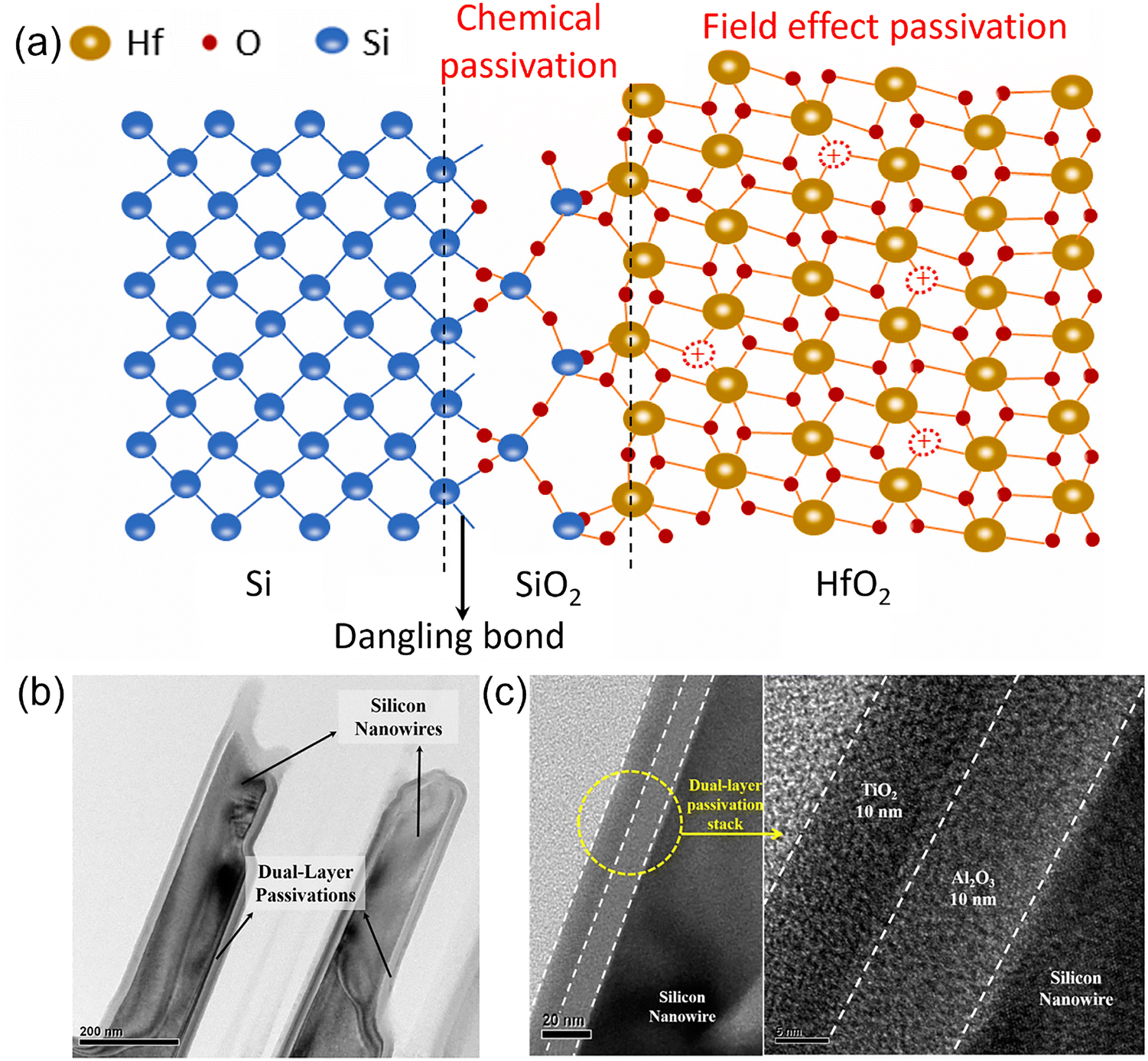 | ||
| Fig. 22 Passivation mechanisms of black silicon and double-layer ALD passivation. (a) Chemical passivation and field effect passivation of black silicon.227 Reproduced with permission from ref. 227. Copyright 2023, Elsevier. (b) Low-magnification TEM image of Al2O3/TiO2 double-layer on SiNWs. (c) High-magnification TEM image of Al2O3/TiO2 double-layer on SiNWs.228 Reproduced with permission from ref. 228. Copyright 2015, American Chemical Society. | ||
| Passivation technique/material | Passivation mechanism | Advantages | Disadvantages | Applicability to black silicon | Typical deposition method |
|---|---|---|---|---|---|
| Si–H surface hydrogenation | Chemical passivation | Effectively saturates dangling bonds; simple process | Thermally unstable; easily desorbed | Useful for temporary or auxiliary passivation | HF treatment, H2 plasma passivation |
| Hydrogenated silicon nitride (SiNx: H) | Field-effect + partial chemical passivation | Low-temperature process; negative fixed charges; also acts as an anti-reflection layer | High interface defect density; often requires an SiO2 interlayer | Commonly used in stacked passivation structures | PECVD |
| Thermal oxidation (SiO2) | Chemical + field-effect passivation | Reliable and well-established; high interface quality; excellent thermal stability | Requires high temperatures (>800 °C); may damage black silicon nanostructures | Effective if black silicon morphology is preserved | Dry/wet thermal oxidation |
| Al2O3 | Strong field-effect + chemical passivation | High negative fixed charge density; excellent for p-type black silicon; good interface passivation | Poor conformity on high-aspect-ratio surfaces; post-deposition annealing needed | Research hotspot; excellent passivation performance | ALD, thermal decomposition, spray coating |
| HfO2 | Field-effect passivation | High dielectric constant; strong field effect; good thermal stability | Complex process; interface defect density needs improvement | Emerging material with potential for high-performance devices | ALD |
| SiO2/SiNx bilayer structure | Combined chemical + field-effect passivation | Combines the advantages of both layers; widely used in commercial solar cells | Interface control complexity; interlayer stress issues | Mature and reliable; suitable for photovoltaic devices | Thermal oxidation + PECVD |
Chemical passivation reduces interface trap density by saturating surface dangling bonds, thereby suppressing non-radiative recombination. Wong et al. studied methyl-terminated (CH3–) Si(111) surfaces prepared via halogenation/methylation,229 the CH3– groups covalently bond to surface silicon atoms. While structurally similar to H-terminated surfaces, CH3–Si(111) exhibits superior resistance to oxidation in air and aqueous environments. Although both Si–H and Si–C bonds show comparable thermal stability in vacuum, CH3– provides a higher kinetic barrier against oxidation. Unlike H–Si(111), whose passivation degrades under ambient conditions, CH3– maintains electronic passivation more stably. Furthermore, alkyl groups induce a surface dipole, modulating the electron affinity and charge transfer at the silicon interface. As a result, CH3–Si(111) demonstrates improved carrier lifetime and surface recombination properties.
In parallel, field-effect passivation provides an additional suppression mechanism by introducing fixed charges within the passivation layer, typically through oxide or dielectric films that establish a built-in electric field. This field repels minority carriers away from the interface, lowering their concentration at the surface and effectively reducing the recombination rate.
More advanced methods include the ALD deposition of high-k dielectrics such as Al2O3 or HfO2, which not only passivate the surface but also contribute to favorable band alignment and field-effect passivation. Among ALD materials, Al2O3 is widely used due to its intrinsic negative fixed charges (1012–1013 cm−2)173,230,231—originating from oxygen interstitials or aluminum vacancies—provide strong field-effect passivation. These negative charges repel minority carriers in p-type or p+-type silicon, thereby suppressing surface recombination. For n-type silicon, ALD HfO2 is a more suitable alternative owing to its positive fixed charge and higher dielectric constant (∼25).232 Its higher refractive index (∼2.1) also enables simultaneous antireflection and passivation, making it promising for efficient black silicon solar cells.
To suppress charge injection into defect states within Al2O3, a thin interfacial layer of ALD-grown SiO2 can be introduced. This interlayer effectively reduces the generation of negative fixed charges within the Al2O3 layer.233,234 The SiO2 layer functions as an electron tunneling barrier, preventing charge injection into trap states within Al2O3. When the interlayer is sufficiently thick, the overall fixed charge density in the SiO2/Al2O3 dielectric stack can even shift to positive values due to the combined effect of fixed and bulk charges in the SiO2 film. This SiO2/Al2O3 stack not only alters the effective charge polarity but also enhances both optical and electrical performance by reducing mid-gap interface defects, partly due to hydrogen diffusion during post-deposition annealing. In addition, the TiO2 layer has a high positive charge density,228 which can adjust the negative charge of Al2O3 to make the double layer structure appear positive and reduce the defect density. The TEM images are shown in Fig. 22(b) and (c).
The influence of various plasma treatments during the ALD process of Al2O3/SiO2 multilayers on silicon surface passivation has been systematically investigated.235 Among them, the most significant improvement was achieved by applying H2 plasma treatment after SiO2 deposition, reducing the surface recombination parameter to as low as 0.35 fA cm−2 on (100)-oriented n-type silicon with a resistivity of 10 Ω cm—over five times lower than the value obtained from Al2O3 single layers without plasma treatment. Different plasmas (H2, N2, O2, N2/H2 mixtures, and Ar) were compared, with particular emphasis on interface modification and dipole formation at Al2O3/SiO2 interfaces, which strengthen field-effect passivation. Post-deposition annealing further enhances passivation by reducing interface defects. At annealing temperatures below 450–500 °C, the effective minority carrier lifetime increases markedly with temperature. At higher temperatures, the lifetime tends to saturate, and the difference between treated and untreated samples becomes more pronounced. Notably, prolonged H2 plasma exposure yields the most substantial enhancement in surface passivation.
In MACE-fabricated black silicon, post-etch cleaning and passivation are vital for improving surface quality and electronic performance. The standard RCA cleaning protocol,225 particularly SC-1, effectively removes porous silicon with high defect density by etching fragile nanostructures while preserving larger features, thereby smoothing the surface—an effect comparable to thermal annealing.236 Despite the increase in surface defect density post-etching (up to ∼7-fold), SC-1 treatment can reduce this to ∼3-fold and significantly enhance minority carrier lifetime by tenfold. Partial passivation is also achieved via residual Si–H and Si–O bonds, with trapped hydrogen remaining stable over months. For further passivation, ALD-deposited Al2O3 provides a uniform, conformal coating even on complex nanostructures. Its high density of negative fixed charges induces strong field-effect passivation, depleting minority carriers at the interface and mitigating the impact of remaining defects. Thus, Al2O3 offers both chemical and field-effect passivation, making it a preferred choice for stabilizing MACE-processed black silicon.
Beyond Al2O3 and HfO2, other ALD-deposited oxides like ZnO, TiO2, and Sc2O3 offer promising results. Song et al. demonstrated that ALD ZnO (∼4 nm) could effectively passivate defect states on nanostructured silicon and modulate hole transport through enhanced surface band bending.237 As the ZnO thickness increased, Si–O coordination likely contributed to further chemical passivation at the Al/nanostructured-Si interface, resulting in ∼24% improvement in power conversion efficiency via the formation of a passivating tunnel contact. In addition, ALD-deposited dielectric oxides such as Al2O3, TiO2, HfO2, and Sc2O3 have shown promise for both optical and electrical optimization.238,239 Finite-difference time-domain (FDTD) simulations revealed improved anti-reflective behavior across a broad spectrum, emphasizing the importance of selecting optimal film thicknesses.
In large-scale applications, SiO2/SiNx bilayer passivation has enabled black silicon solar cells with higher performance.186,240–242 SiO2 and SiNx are generally prepared by thermal oxidation and plasma-enhanced chemical vapor deposition (PECVD). The ratio of Si to N in SiNx has a significant impact on performance.243 Si-rich SiNx films exhibit increased Si–Si and Si–H bonds, enhancing chemical and bulk passivation by saturating dangling bonds and facilitating hydrogen diffusion during annealing. The reduction in N–H bonds and nitrogen back-bonding lowers fixed positive charge density, weakening field-effect passivation. In contrast, N-rich SiNx films possess higher fixed charge density and stronger field-effect passivation but suffer from increased interface defect density, limiting chemical passivation. For p-type silicon, SiNx induces strong inversion, whereas SiOx yields only depletion or weak inversion.
In summary, effective surface passivation is essential for mitigating surface recombination and unlocking the full optoelectronic potential of black silicon. From chemical cleaning and hydrogen termination to advanced dielectric coatings such as Al2O3, SiO2, and SiNx, each strategy offers distinct advantages rooted in chemical and field-effect mechanisms. The interplay between fixed charges, interface defects, and hydrogen dynamics defines the overall passivation performance. As black silicon technologies continue to evolve toward high-efficiency and low-cost applications, optimizing passivation schemes tailored to specific device architectures and fabrication routes will remain a critical research focus.
4. Tunable properties and functional applications enabled by micro–nano surface engineering: physical, chemical, and biological
The micro- and nanostructures on the surface of black silicon fundamentally alter its material properties, enabling a wide range of advanced functionalities. These structures enhance light absorption by inducing multiple internal reflections within the micro- and nanostructures, significantly reducing surface reflectivity. When doped with impurities that introduce new energy levels, black silicon's absorption spectrum extends into the infrared region, further broadening its spectral response. The morphological modifications not only enhance optical properties but also improve optoelectronic efficiency, field emission characteristics, and photocatalytic activity.244 Moreover, black silicon's unique surface structures have enabled applications in antimicrobial coatings,245 superhydrophobic surfaces, and surface-enhanced Raman scattering (SERS) devices, demonstrating its versatility across various fields.4.1. Optical properties
The most prominent feature of black silicon is its greatly enhanced light absorption, which is a direct result of its unique surface morphology. The micro- and nanostructures on the silicon surface facilitate multiple light-scattering and trapping effects,99,246–248 significantly reducing surface reflectance and enabling near-total absorption across a wide wavelength range. Beyond this, the altered surface also introduces a high defect density that promotes carrier recombination, making black silicon an effective photoluminescent material. These surface-induced changes not only improve its optical properties but also extend its potential for diverse applications. Extensive research has focused on understanding the relationship between the surface morphology of black silicon and its optical behavior. | ||
| Fig. 23 Optical absorption properties of black silicon. (a)–(d) Light absorption by different micro- and nano structures in black silicon. (a) Polished silicon. (b) Nanostructured silicon. (c) Microstructured silicon. (d) Nano and micro hybrid black silicon. (e) Reflection spectra of planar and textured silicon surface.65 Reproduced with permission from ref. 65. Copyright 2020, John Wiley & Sons. (f) Polarization insensitivity of black silicon.90 Reproduced with permission from ref. 90. Copyright 2018, Elsevier. (g) Reflection spectra of black silicon processed at different annealing temperatures for two-step MACE.122 Reproduced with permission from ref. 122. Copyright 2014, Springer Nature. (h) Reflection spectra of black silicon with/without QDs.250 Reproduced with permission from ref. 250. Copyright 2020, Elsevier. | ||
Doping during the laser ablation process improves the light absorption properties of black silicon. The optical absorption of black silicon prepared in corrosive gases reaches 95% for photon energies above the bandgap, whereas samples processed in inert gases exhibit absorption of 90%.73 NIR broadband light absorption is achieved when the sulfur concentration exceeds 0.6% (about 1020 atoms cm−3). For wavelengths exceeding 1100 nm, the absorption of black silicon fabricated in an SF6 atmosphere decreases slightly (by ∼5%). In contrast, in samples prepared in other gas environments, the absorption drops sharply, even below that of flat silicon, indicating very poor infrared absorptivity. Sulfur impurity doping is confirmed as the key to enhanced infrared absorption.58,72,251 Other doping elements, such as tellurium (Te), selenium (Se), N, Au, etc., and their effects will be described in Section 4.3.
Simulation studies show that by adjusting the doping level and surface morphology, the light absorption range of black silicon can be extended to wavelengths as long as 20 µm.67 Black silicon with a high aspect ratio (∼30:1) and heavy doping forms an efficient conical metasurface that suppresses reflection across a broad spectral range. The absorption exceeds 99.5% in the range of 1–8 µm and remains beyond 90% up to 20 µm.
The light absorption of black silicon depends on the incident wavelength and is not sensitive to factors such as light polarization.90 Combined with its low reflectivity and high sensitivity, these features make black silicon a promising material for broadband optoelectronic applications. As shown in Fig. 23(f), the surface roughness enhances scattering and strengthens the interaction among light waves with different polarization states, enabling the structure to behave effectively as a homogeneous medium.
Zhang et al. investigated the effect of Ag nanoparticles on the near-infrared light absorption of black silicon fabricated by two-step MACE.122 Ag nanoparticles were obtained by rapid thermal annealing of Ag films, with the increase of annealing temperature, the size of the nanoparticles grew and the interparticle spacing increased, thereby affecting the reflectivity, as shown in Fig. 23(g). After plasma treatment, black silicon exhibited a maximum absorption of 93.6% within the near-infrared spectrum (820–2500 nm) and maintained an average absorption of 91.8% across the range of 250–2500 nm. The extensive absorption in the near-infrared region is primarily attributed to plasmon resonance frequency shifts due to particle size, high refractive index, and interparticle coupling. The uneven distribution of Ag nanoparticles results in the plasma-enhanced absorption peak in the NIR range being a composite of multiple peaks. As the incident wavelength lengthens, the decay rate of free electrons in the dielectric constant of Ag accelerates, shortening the plasma lifetime and widening the resonance bandwidth.
Both single-metal and bimetallic nanoparticles can significantly enhance anti-reflective performance.13 Bimetallic nanoparticles exhibit superior anti-reflective performance across a broader spectral range compared to single-metal nanoparticles. This is attributed to their wider size and shape distribution, higher surface roughness, and multiple surface plasmon resonance effects. To investigate the anti-reflective effects of metal nanoparticles, researchers modified laser-textured silicon surfaces with Ag, Ag–Au bimetallic, and Cu–Ag–Au trimetallic nanoparticles via thermal annealing. Within the wavelength range of 300 to 1200 nm, the average reflectance of the laser-textured Si surface was 8.3%, while the average reflectance of surfaces decorated with Ag–Au and Cu–Ag–Au nanoparticles decreased to 6.9% and 5.5%, respectively. The decoration with ternary metal NPs resulted in better broadband anti-reflective performance.
In addition, quantum dots play an important role in improving light absorption. For instance, silicon quantum dots (SiQDs)/black silicon hybrid nanostructures reduce reflection across a broad spectrum (300–1000 nm),250 and the reflection spectrum is shown in Fig. 23(h). The SiQDs with an average diameter of 1.8 ± 1.1 nm can convert the UV light into visible light, reducing reflection from 9.9% to 6.5% at 600 nm, with even greater reductions at longer wavelengths. In another research, SiC colloidal quantum dots were used as down-conversion materials to perform the same role as SiQDs,255 converting UV light into visible light. Additionally, quantum dots coated on the surface of SiNWs increase the photoconductivity effect, reducing the surface recombination rate.
 | ||
| Fig. 24 PL spectra of black silicon under different femtosecond-laser processing parameters. (a) Different scanning velocities. (b) Different laser fluences.256 (c) Unannealed sample and samples annealed at different temperatures.257 (d)–(e) O/Si atomic ratio for different scan velocities and laser fluence.256 (f) PL spectrum of laser-treated black silicon before and after KOH etching.257 (a), (b), (d) and (e) Reproduced with permission from ref. 256. Copyright 2011, AIP Publishing. (c) and (f) Reproduced with permission from ref. 257. Copyright 2013, Optica Publishing Group. | ||
The black silicon fabricated by RIE has PL bands in both the visible and infrared regions.258 As the temperature drops from room temperature to 10 K, the visible light bands show a large blue shift from 696 nm to 560 nm. In the infrared region, PL bands centered at 1.14 µm and 1.53 µm are observed, with the former attributed to band-to-band carrier recombination in silicon and the latter to defect-related luminescence.
PL signals were observed only in thermally annealed samples, as shown in Fig. 24(c), highlighting the critical role of annealing in luminescence devices.257 Structural defects and impurities induce a non-radiative recombination process that quenches the PL signal through mobility-induced band-tail state quenching.259 As the annealing temperature increases, the PL intensity rises significantly. This is attributed to strain during annealing, which alters impurity and defect energy levels and can even modify the bandgap structure of black silicon. Fig. 24(f) shows the PL spectrum of laser-treated black silicon before and after KOH chemical etching. After etching, sulfur impurities on the surface layer are removed, and the PL intensity increases, indicating that the luminescence of black silicon is not caused by impurities. Additionally, high-temperature annealing reduces non-radiative defect channels, improving optical performance by allowing more carriers to occupy shallow energy levels near the surface, thereby enhancing luminescence.
The surface plasma treatments can also enhance the luminous efficiency.252,260 Black silicon and Ag nanoparticles were employed to improve the electroluminescence (EL) intensity of silicon nanocrystals (Si-ncs) in light-emitting diodes (LEDs).260 The black silicon was formed by a two-step MACE, and then the Si-ncs were deposited on it. Samples etched for 5 minutes had the lowest reflectivity and the highest surface roughness. Ag nanoparticles generate surface plasmons that enhance the local electromagnetic field, increasing the excitation probability of Si-ncs and thereby boosting EL intensity. Simultaneously, the textured surface of black silicon enhances charge injection efficiency and light emission by reducing surface reflection and improving light trapping. Specifically, the EL intensity of Si-ncs LEDs increased by 3.2 times with black silicon etched for 5 min and by 4.9 times with Ag nanoparticles annealed at 200 °C. Combining black silicon and Ag surface plasmons achieved a maximum EL enhancement of 8.5-fold, showcasing the synergistic effect of morphology optimization and plasmonic enhancement.
4.2. Electrical properties
Black silicon exhibits distinctive electrical characteristics that are crucial for assessing its performance across various applications. Its key properties include parameters such as carrier concentration, carrier mobility, activation energy, and impurity concentration. These attributes determine the material's efficiency of electrical conduction and photoelectric interactions, directly impacting its performance in photovoltaic solar cells, photodetectors, and sensors.The surface morphology of black silicon significantly affects its electrical properties. Increased surface roughness leads to greater carrier scattering, reducing carrier mobility. Additionally, the high surface area introduces more defect states that trap carriers, further hindering carrier migration. Heavily doped black silicon films with supersaturated sulfur impurities demonstrate low carrier activation energies, resulting in a weak temperature dependence of carrier concentration and mobility.261,262 Moreover, black silicon generally has a shorter carrier lifetime than conventional silicon. This reduction is mainly attributed to the quantum confinement effect—where electron and hole wave functions overlap in a confined volume and the high defect density in the surface microstructure.164 These nanostructures increase carrier recombination rates at the surface, influencing the minority carrier lifetime.
By carefully controlling surface morphology, researchers can optimize the electrical properties of black silicon to align with the specific needs of diverse applications. Thermal annealing is a common method employed to extend the carrier lifetime, but it often induces metal contamination, dopant diffusion, and other adverse effects. As a result, the lifetime of silicon after laser radiation cannot be restored solely through thermal annealing. Chemical acidic etching after laser treatment is an effective method for eliminating laser damage. This process can significantly increase the minority carrier lifetime. The carrier lifetime of black silicon samples with different laser fluences (Fig. 25(a)) was measured by quasi-steady-state photoconductance (QSS-μPCD).79Fig. 25(b) shows the minority lifetime maps of the samples. The carrier lifetime of black silicon gradually increases with prolonged etching time, indicating that the laser-induced defects are confined near the surface, and the lifetime remains unchanged after 30 s. A smaller laser fluence leads to a longer carrier lifetime, but extended etching times may reduce light absorption efficiency. A more intuitive result is shown in Fig. 25(c). Therefore, it is necessary to find an optimal balance between these factors. An etching duration of 10 s achieves a high absorption rate of 90.5% and a carrier lifetime of 2 ms. Similarly, significant surface damage caused by pattern transfer during plasma etching can also be eliminated through appropriate damage/defect removal etching,72,263 thus effectively extending carrier lifetime.
 | ||
| Fig. 25 The change of lifetime with different etching and passivation conditions. (a) A photograph of a laser-treated silicon wafer, with dark circles in the upper-left, upper-right, and lower-left indicating laser fluences of 5.4, 4.3, and 3.2 kJ m−2, respectively. (b) Lifetime maps of QSS-μPCD with varying etching time in (a). (c) Variation of maximum absorptance (250–1100 nm) and effective minority-carrier lifetime at an excess carrier density of 1.0 × 15 cm−3 as a function of etching time.79 Reproduced with permission from ref. 79. Copyright 2022, IEEE. (d) SEM image of black silicon after Nafion solution passivated. (e) Minority carrier lifetime of black silicon before and after Nafion passivation.46 Reproduced with permission from ref. 46. Copyright 2022, John Wiley & Sons. | ||
Surface passivation has also been demonstrated as an effective method for extending the carrier lifetime of black silicon. While long nanowires provide high specific surface areas, they introduce numerous dangling bonds that can impair optical and electronic properties. Shorter nanostructures, in contrast, are easier to passivate, leading to superior surface passivation and enhanced device performance.264 Chen et al. used a Nafion solution to passivate black silicon nanowires fabricated by MACE.46 The nanowires were 160–320 nm long with pore widths of 50–200 nm. Passivation was performed by spin-coating the Nafion solution, which filled most of the nanopores and reached the bottom of the nanowires (Fig. 25(d)), most of the outer-shell defects were passivated. After passivation, as shown in Fig. 25(e), the effective minority carrier lifetime increased from 3.8 µs to 1.1 ms for nanowires with a length of 160 nm and to 0.6 ms for nanowires with a length of 320 nm on a planar wafer. When exposed to oxygen, the lifetime further increased from 1.1 ms to 2.4 ms. A similar phenomenon was observed on pyramid-textured wafers, although the carrier lifetime was shorter. With increasing Nafion concentration, the minority carrier lifetime of long nanowires that were difficult to infiltrate initially increased and then decreased. Seref Kalem used acid vapor to smooth black silicon nanowires, effectively reducing and passivating surface defects.164 During this process, the oxides on the surface were removed and new oxides were generated, but the larger defects, such as kinks and interface defects, were eliminated. This study also proves that surface recombination is more important than recombination in the bulk cores and interfaces. Other passivation layers, such as Al2O3, SiNx, TiO2, are also widely used for black silicon,94,125,265–267 providing lower reflectivity and higher carrier lifetime.
4.3. Optoelectronic properties
Black silicon exhibits remarkable optoelectronic properties, making it a valuable material in advanced photonic and electronic applications. The optoelectronic performance of black silicon is intricately linked to its surface morphology, including the size, shape, and spatial distribution of nanostructures, which dramatically alter light absorption, carrier generation, and transport characteristics.268–270 By precisely engineering the morphology of black silicon, researchers can enhance its optoelectronic properties to suit specific applications.Doping is a highly effective method to extend the absorption range of black silicon. By introducing impurities, additional new energy levels are created within the silicon bandgap, enabling black silicon to absorb photons with lower energy, including those in the infrared range. This expanded absorption spectrum enhances the overall light-harvesting efficiency, making the material more suitable for applications like infrared photodetectors and solar cells. However, superdoping will lead to a high impurity concentration (5 × 1019 cm−3) in silicon,45,276 which will produce a large number of background-free carriers, and strong free carrier absorption does not support photoelectric conversion. At the same time, impurity atoms will also cause strong ionized impurity scattering, resulting in a lower light absorption rate. Zhao et al. developed an N+–N− photodetector by laser-modified silicon and ordinary silicon,45 achieving a high response in the NIR range. The absorptance curves are shown in Fig. 26(a), and the inset is the image of the N+–N− photodetector. The responsivities of different reverse biases are shown in Fig. 26(b), and the device exhibited lower responsivity compared to commercial silicon photodetectors under zero bias. However, as the reverse bias increases, the responsivity will be enhanced, attributed to the photoconductive gain. Au has high solid solubility when doped into silicon and can be uniformly distributed with a stable valence, effectively reducing the lattice mismatch and dislocation centers.277 After annealing at 800 °C, the black silicon has an absorption of 95% across 200–1100 nm range. The intermediate energy level introduced by over-doping still maintains a 75% absorption in the 1100–2500 nm range. The photodetectors’ photoelectric response and on/off ratio in the infrared band are more than 10 times higher than those of unprocessed silicon.
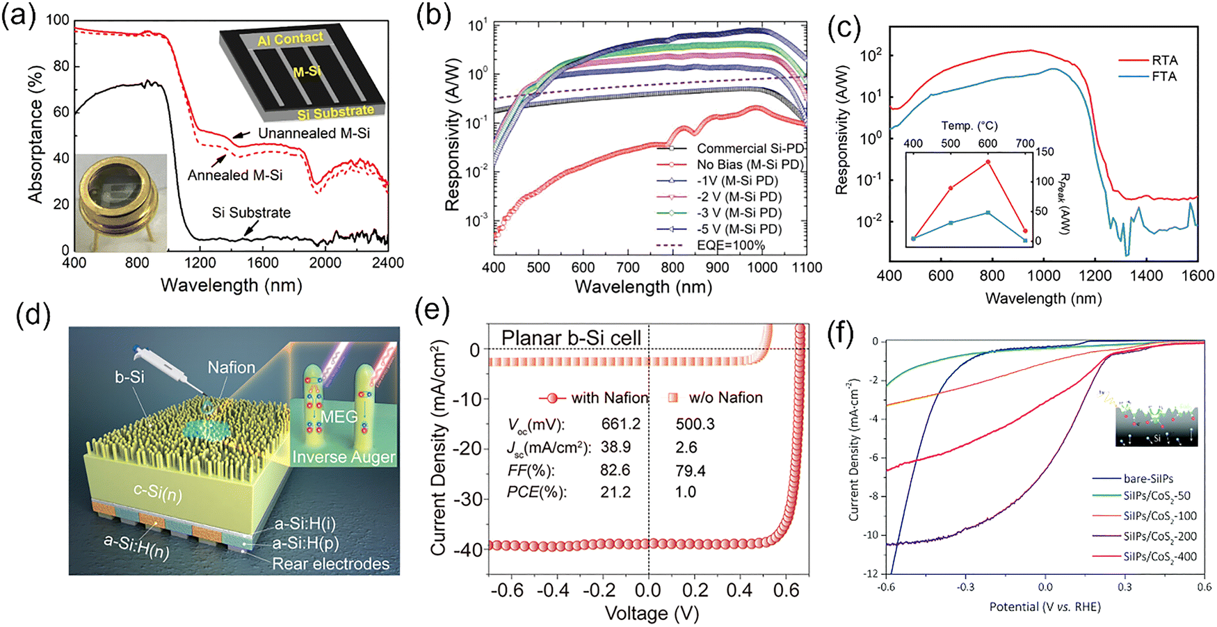 | ||
| Fig. 26 Characterization of photoelectric properties of black silicon. (a) Absorptance of pure Si substrate, laser-modified silicon (M-Si) samples before and after annealing. The inset is the schematic and real image of the M-Si photodetector. (b) Responsivity of M-Si photodetector at different reverse biases, the commercial silicon-PD is shown inset for reference.45 Reproduced with permission from ref. 45. Copyright 2018, IEEE. (c) Influence of RTA and FTA, the inset shows the changes of peak responsivity with temperature.199 Reproduced with permission from ref. 199. Copyright 2020, John Wiley & Sons. (d) Schematic of Nafion passivated black silicon solar cells. (e) J–V curve with and without Nafion passivated planar black silicon solar cell.46 Reproduced with permission from ref. 46. Copyright 2023, John Wiley & Sons. (f) J–t curve (HER) of silicon pyramid array/CoS2 photocathode at 0 V, the inset is a schematic of the photocatalysis process.278 Reproduced with permission from ref. 278. Copyright 2020, Royal Society of Chemistry. | ||
Adjusting the type and concentration of doped atoms is also one way to improve the performance of black silicon photodetectors. Sulfur and nitrogen impurities co-doped black silicon were successfully fabricated using a femtosecond laser in mixed N2/SF6 atmospheres,136 exhibiting excellent infrared absorption stability. Increasing the nitrogen content reduces the sheet carrier density because nitrogen predominantly forms neutral pair defects. The resultant photodetector achieved a responsivity of 58 mA W−1 at 1.31 µm. Te-hyperdoped black silicon photodiodes were also fabricated,76 and the influence of substrate temperature was studied. Increasing the substrate temperature leads to a higher doping concentration gradient, improved lattice quality, and reduced defect density, which together help suppress the dark current of the photodiode. The device exhibited significantly enhanced responsivity compared with commercial silicon photodetectors, particularly in the near-infrared region.
The intrinsically high recombination rate associated with black silicon's textured surface can be mitigated by depositing passivation layers.279 The SiNx/Al2O3 stacks have emerged as particularly effective owing to the chemical hydrogenation of the strong Si–O coordination and hydrogenation passivation at the silicon/Al2O3 interface.280 Zhao et al. reported that the black silicon prepared by sulfur-doped femtosecond laser irradiation exhibited absorptance exceeding 85% in the range of 0.2–2.5 µm due to impurity-level-induced sub-bandgap absorption.281 Then the SiO2 passivation layer is introduced to reduce the background free carrier concentration and structural defects, resulting in prolonging carrier lifetime and enhancing device stability, the responsivity of black silicon device reaches 367 mA W−1 at a bias voltage of 10 V and a wavelength of 1030 nm, which is significantly higher than that of planar silicon (47 mA W−1) under the same conditions.
Annealing is another effective method to reform the recombination rate. Huang et al. fabricated a photodetector based on the black silicon prepared by femtosecond laser irradiation in SF6 environment,199 by applying rapid thermal annealing (RTA) and hydrogenated amorphous silicon passivation, the device achieved photoelectric response up to 1600 nm. The peak responsivity (∼1100 nm) reached 215.69, 497.51, 679.84, 956.62, and 1097.60 A W−1 under reverse bias voltages of 1.5, 5, 8, 15, and 20 V, respectively. The authors claimed an improvement of nearly three orders of magnitude, with particularly high responsivity maintained in the telecommunication wavelength range (1260–1600 nm) compared to commercial Si and Ge photodetectors under comparable bias (below 1 A W−1 at similar wavelengths). Fig. 26(c) illustrates the performance differences between conventional furnace thermal annealing (FTA) and RTA, with the latter demonstrating superior results. RTA was found to inhibit the diffusion of sulfur atoms while activating the carrier to repair structural defect damage, and passivation can effectively inhibit the high dark current caused by suspension bond defects on the material surface. Su et al. also used RTA to improve the performance of metal-semiconductor–metal photodetectors in N2 ambient,282 the tensile stress and point defects are eliminated, leading to a huge improvement of carrier mobility, conductivity, and carrier concentration, thus yielding almost 3 orders of magnitude increase in responsivity, reaching 76.8 A W−1 for the sample annealed at 673 K, compared with 0.032 A W−1 for the unannealed device at a wavelength of 600 nm. Laser annealing provides an alternative route, offering localized heating that yields highly crystalline, stress-free phases while preserving the strong absorptance characteristic of black silicon.60,283 Kearney et al. treated sulfur-hyperdoped black silicon with ultrashort laser pulses,284 demonstrating that ultrafast laser heating can reactivate sub-bandgap absorption that had been quenched by prior thermal annealing, while simultaneously retaining high crystallinity and stable rectifying behavior.
DRIE and PIII are combined to produce black silicon by Zhong et al.,285 the improved doped sulfur element introduces multiple defect levels and form impurity bands on the silicon surface, reducing the silicon bandgap from 1.12 eV to ∼1.0 eV, and the light absorption was enhanced, especially in the NIR range (800–2000 nm), the maximum absorption rate reached 83%. The silicon-PIN photodetector, featuring microstructured black silicon on its backside, demonstrated excellent device performance, achieving a responsivity of 0.53 A W−1 at 1060 nm. Li et al. employed a dual-step strategy combining ion implantation with pulsed-laser reactivation to prepare Ar-doped black silicon photodetectors.286 Pulsed laser irradiation after ion implantation can not only serve as a post-annealing step to improve the crystal quality of the implanted layer, but also enable further Ar superdoping to enhance infrared absorption. The resulting dual-contact photodiode achieved responsivities of 0.975 A W−1 at 1.31 µm and 1.28 A W−1 at 1.55 µm.
The solar cell made of black silicon prepared by PIIIE for the first time in 2011 (device area: 125 × 125 mm2) has a conversion efficiency of 15.68% and a fill factor (FF) of 0.783,22 then Zhong et al. prepared nanostructured surfaces of different heights by PIIIE,81 a maximum conversion efficiency of 15.99% was achieved at a height of 300 nm (device area: 156 × 156 mm2), which was the competition result between reduced reflectivity and loss of internal quantum efficiency (IQE). It remains a disadvantage in contact with the electrode and black silicon, but the conversion efficiency can be further improved by surface passivation and preparation of better contact.
Ye et al. reported the first perovskite/silicon tandem cell using industrial-grade black silicon and tunnel oxide passivation contacts.198 The silicon substrate was textured via MACE and then smoothed by alkaline treatment, which reduces the surface area and removes a large portion of defects. Black silicon undergoes surface reconstruction to provide passivation while retaining the broadband light capture. Due to its unique low polarity and high dispersion components, the reconstructed black silicon improves perovskite wettability and enhances adhesion between subcells. Perovskite grown on the reconstructed black silicon exhibits highly crystalline properties and achieves vertically aligned grain boundaries through nanoconfinement, thereby reducing unwanted carrier recombination losses and promoting charge collection at both contacts. These advancements significantly improve JSC and FF in series, ultimately resulting in a certified PCE of 28.2%.
Sun et al. mitigated surface recombination in black silicon solar cells by incorporating silane-based additives into the PEDOT: PSS organic layer.296 Through covalent Si–O–Si bonding, both interfacial adhesion and overall electrical contact between PEDOT:PSS and the nanostructured silicon were improved. By adjusting the composition ratio of silane chemicals in PEDOT:PSS, a balance was achieved between light capture and surface-to-volume ratio, resulting in a maximum Voc value of 640 mV and a PCE of 14.1% (substrate area: 15 × 15 mm2). Additionally, the lifetime of silicon minority carriers was enhanced.
In another study, blade-coated wide-bandgap perovskite films were applied to double-textured silicon at the submicron scale to achieve high-efficiency perovskite/silicon tandem solar cells.297 In this configuration, the perovskite cell “flattens” the textured silicon surface by filling the valleys between the pyramids. This texturing extends the path length of light within the silicon, achieving a matched Jsc exceeding 19 mA cm−2 and an efficiency of 26%.
Surface passivation has been further shown to significantly enhance device performance. In 2015, Savin et al. prepared nanostructures approximately 800 nm in height and 200 nm in width using low-temperature DRIE,23 and passivated the surface with a 20 nm Al2O3 thin film to fabricate a thick interdigital back contact (IBC) solar cell with a device area of 9 cm2. The IBC cell demonstrated an open-circuit voltage (Voc) of 665 mV, a short-circuit current density (Jsc) of 42.2 mA cm−2, an FF of 78.7%, and a power conversion efficiency (PCE) of 22.1%. This advancement marked a breakthrough in mitigating surface recombination in black silicon and achieving high conversion efficiency without damaging light absorption, further expanding the applicability of black silicon in solar energy.
In Zhou's research, organic-passivated black silicon solar cells were fabricated on both planar and pyramid silicon wafers.46 The device structure and corresponding I–V curves are shown in Fig. 26(d) and (e). On a planar silicon wafer, Nafion passivation significantly enhanced device performance, the Voc, Jsc, FF, and PCE after Nafion passivation were 661.2 mV, 38.9 mA cm−2, 82.6% and 21.2% (device area: 142 cm2), respectively, compared with the unpassivated counterparts (Voc = 500.3 mV, Jsc = 2.6 mA cm−2, FF = 19.4% and PCE = 1.0%). A similar improvement was observed for pyramid black silicon cells. In another study, Hsu et al. employed SiNx and Al2O3 to passivate MACE-processed black silicon on a pyramidal substrate, achieving an optimal conversion efficiency of 22.9% and a remarkably low surface recombination velocity of 42 cm s−1.264
A core–shell heterojunction structure consisting of SiNW arrays and carbon quantum dots (CQDs) was reported by Xie et al.298 The barrier height of this structure was 0.75 eV, providing a good rectifying effect. When used as a solar cell, the device exhibited a Voc of 0.51 V, a Jsc of 30.09 mA cm−2, a FF of 0.593, and a PCE of 9.10%. Graphene quantum dots (GQDs) were used as down-conversion materials in the interface layer of black silicon solar cells prepared via MACE to achieve good band alignment between graphene transparent-conductive electrodes and silicon.299 By doping graphene transparent-conductive electrodes, passivating the silicon back surface, and introducing GQDs into the interface layer, the GQD layer functioned not only as a hole-transport layer but also as an electron-blocking layer, thereby reducing carrier recombination within the device. The maximum PCE reached 13.66% (device area: 9 mm2). The cell also exhibited excellent long-term stability, maintaining 84% of its original PCE after being exposed to air for 30 days.
The inverted silicon pyramid array (SiIP) photocathode can generate a photogenerated voltage of 440 mV and exhibits a high photocurrent density.278 Moreover, its quasi-hydrophilic feature allows for a higher photocurrent density under large reverse bias. The intrinsically slow charge-transfer kinetics of the SiIP photocathode can be further enhanced with the incorporation of cobalt disulfide (CoS2) nanocrystals. As shown in Fig. 26(f), the initial potential of the SiIP/CoS2 photocathode was 0.22 V, and the saturation photocurrent density reached 10.4 mA cm−2. The water-splitting performance can be further improved by using higher-quality silicon wafers and other high-performance catalysts. Yu et al. used a TiO2 coating layer to passivate the black silicon surface,17 and a saturated photocurrent density of 32.3 mA cm−2 was generated by a black silicon/TiO2/cobaltous hydroxide (Co(OH)2) heterostructured photoanode. This combination extended the lifetime of black silicon to four hours, markedly improving the system stability during water-splitting reactions. Gu et al. compared the application of columnar and sinuous nanoporous black silicon in the photoelectrochemical hydrogen production process.301 Due to the damaged diffusion channels of oxygen on the surface of the sinuous nanoporous black silicon, silicon oxide formation is suppressed in an oxygen-deficient environment, leading to higher stability than the columnar black silicon under different conditions, suggesting the feasibility of controlling the subsurface morphology to extend the stability of the photoelectrode.
Molybdenum disulfide (MoS2) is a widely studied two-dimensional material with strong catalytic activity at its edges. Molybdenum sulfide quantum dots (MoSx) have highly exposed edges due to their nanoscale size, which can be combined with black silicon to achieve higher catalytic activity. Wang et al. modified the black silicon surface prepared by MACE with amorphous MoSx.302 This modification not only introduced more active sites to enhance electrocatalytic activity but also served as a surface passivation layer, mitigating the etching effect of the acidic electrolyte during operation. The resulting device exhibited excellent catalytic performance, with an onset potential of 0.255 VRHE, a high Jsc of 12.2 mA cm−2, and a hydrogen evolution rate of 226.5 µmol h−1 cm−2. It also demonstrated strong operational stability over 8 hours of continuous operation.
Beyond hydrogen evolution, black silicon shows a distinctive advantage for the chemical synthesis of ammonia (NH3), a major focus in catalysis research.303–305 Wang et al. reported a photoelectrochemical N2 reduction reaction route combining black silicon and AgNPs to synthesize NH3,306 the NH3 evolution reaction activity was enhanced, achieving an NH3 yield of 2.87 µmol h−1 cm−2. Muataz et al. described a solar-driven nanostructured photoelectrochemical cell for the conversion of atmospheric N2 to ammonia,49 exhibiting a yield of 13.3 mg m−2 h−1 under 2 suns illumination. The ammonia yield of unetched planar silicon was only 11% of the gold nanoparticle/black silicon/chromium structure. The markedly enhanced performance results from the large surface area, low reflectivity, and improved hole transport provided by the black silicon nanostructures.
4.4. THz/Field emission characteristics
In contrast to planar silicon with a relatively large penetration depth, black silicon significantly reduces the light penetration depth to the submicron scale due to its microstructured surface. The enhanced multiple light scattering and the confinement of photogenerated carriers within these nanostructures lead to significant modulation of the local potential. As a result, black silicon exhibits surface anisotropy, which can induce polarization effects that produce terahertz (THz) emission.50 The enhanced THz emission is illustrated in Fig. 27(a),307 where the THz polarization direction is perpendicular to the interface. The polarization amplitude is directly proportional to the local intensity of the laser beam. However, oblique incidence leads to a linear phase gradient along the X-axis, resulting in a local pulse delay. The frequency range of the THz wave is 0.1–10 THz (1 THz = 1012 Hz), corresponding to wavelengths from 0.03 mm to 3 mm, falling between the millimeter-wave and infrared regions of the electromagnetic waves. Fig. 27(b) shows the experimental setup of THz emission. THz emission is observed only from damaged or rough surfaces, whereas polished silicon does not exhibit measurable THz emission. Fig. 27(c) further demonstrates that black silicon produces significantly higher THz emission than either damaged or unpolished silicon surfaces.50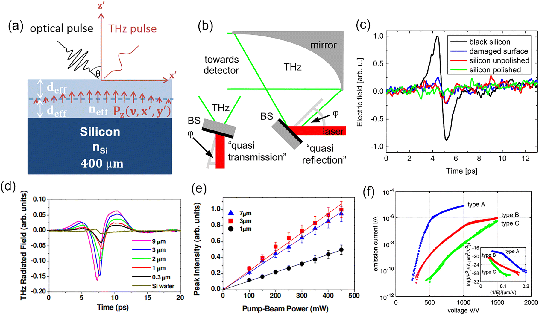 | ||
| Fig. 27 Emission characteristics of black silicon. (a) The enhancement mechanism of THz emission.307 Reproduced with permission from ref. 307. Copyright 2017, Optica Publishing Group. (b) Schematic of THz emission setup. (c) The THz electric field for black silicon, damaged surface, unpolished silicon, and polished silicon.50 Reproduced with permission from ref. 50. Copyright 2008, AIP Publishing. (d) Time-domain waveform of silicon wafer and SiNWs with lengths from 0.3 µm to 9 µm. (e) Intensity of THz emission with different SiNWs length and pump-beam power.114 Reproduced with permission from ref. 114. Copyright 2010, Optica Publishing Group. (f) Field emission I–V curves of three silicon samples: type A (black silicon with 20 µm pillars), type B (black silicon with 8 µm pillars), and type C (planar black silicon).308 Reproduced with permission from ref. 308. Copyright 2016, AIP Publishing. | ||
Blumröder et al. studied the THz emission of black silicon fabricated by RIE,307 the pulse width of the THz wave is on the order of picoseconds, so the carrier capture occurring on this timescale can significantly enhance the THz emission. The micro-morphology of the black silicon surface can effectively increase the THz emission, and its amplitude depends on the structure geometry and the depth of the silicon nanostructure, with deeper microstructures leading to stronger emission and slightly wider pulses. This enhancement is attributed to the increased number of carriers produced directly within the silicon needle, where the resulting THz radiation is effectively outcoupled. A similar phenomenon was observed by Jung et al., who used MACE to fabricate SiNW arrays and tested the THz emission performance,114 as shown in Fig. 27(d) and (e), longer SiNW arrays and higher pump-beam power resulted in stronger THz emission.
In addition to THz emission, black silicon can also be used to prepare field-emission devices.308–310 Langer et al. prepared a black silicon field emission column array on a p-type silicon substrate by RIE.308 As shown in Fig. 27(f), samples with a column height of 20 µm (type A) exhibited a low turn-on field of 6.4 V µm−1, with a field enhancement factor of 800 and an emission current reaching 8 µA at an applied field of 20 V µm−1. Moreover, taller silicon columns improved the emission stability, indicating that such structures can serve as promising alternatives to traditional silicon-tip field-emission arrays.
4.5. Surface-enhanced Raman scattering effect
SERS is a special Raman scattering phenomenon that occurs on some special substrates consisting of noble-metal nanostructures (Au, Ag, Cu, etc.).191,311 The Raman scattering intensity of molecules can be significantly enhanced due to the localized surface plasmon resonance (LSPR) effect, which greatly improves the specificity and sensitivity of Raman detection.312 Nanoparticles stabilized in colloidal solutions are commonly used in SERS analysis, which provides strong signal enhancement in Raman signals. However, they are vulnerable to environmental changes and contamination, and the disordered arrangement of nanoparticles results in poor reproducibility.313,314 Other approaches, such as direct production or in situ growth of noble-metal nanostructures, are not cost-effective.315–317 Black silicon has been used as a SERS-active substrate in recent years due to its low cost and reusable features,128,318 and its SERS performance can be further boosted through precise engineering of both the black-silicon nanostructure and the deposited metal layer.35 The enhancement factor (EF) is calculated as follows:319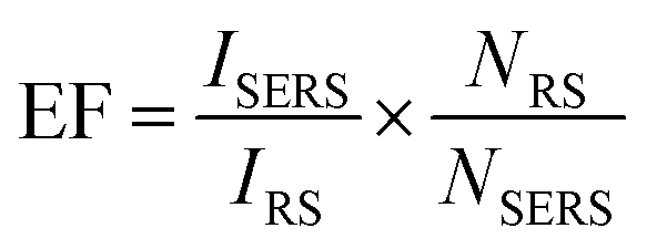 | (4.1) |
It is generally believed that SERS arises from the synergistic effect of electromagnetic enhancement, resulting from the synergistic contributions of electromagnetic enhancement, arising from the amplification of the local electromagnetic field near the substrate surface, and chemical enhancement, which results from interactions between adsorbed molecules and the substrate. The Raman signal intensity is proportional to the fourth power of the local field EF.312
The thickness of the surface metal nanolayer has a great influence on the SERS signal. As shown in Fig. 28(a),267 no Raman peaks are observed in the absence of metal nanoparticles. Black silicon exhibits higher SERS intensity than textured silicon, and the maximum spectral enhancement is achieved at an optimal Ag nanoparticle size. Here, the nanoparticle size is determined by the deposited Ag mass thickness during thermal evaporation. For instance, mass thicknesses of 3 nm, 5 nm, and 10 nm result in Ag nanoparticles with average diameters of ∼10 nm, ∼18 nm, and ∼25 nm, respectively. With increasing size, the localized surface plasmon resonance peak undergoes a red shift and broadening, since higher-order multipole modes are excited in addition to dipolar scattering, which in turn affects light-trapping efficiency. In another study, the SERS substrates were fabricated by first preparing silicon inverted pyramids via Ag MACE, subsequently decorated with AgNPs using electroless deposition and radiofrequency sputtering.320 Compared with electroless deposition, radiofrequency sputtering produces smaller and denser nanoparticles on the black silicon surface, thereby yielding stronger SERS enhancement.
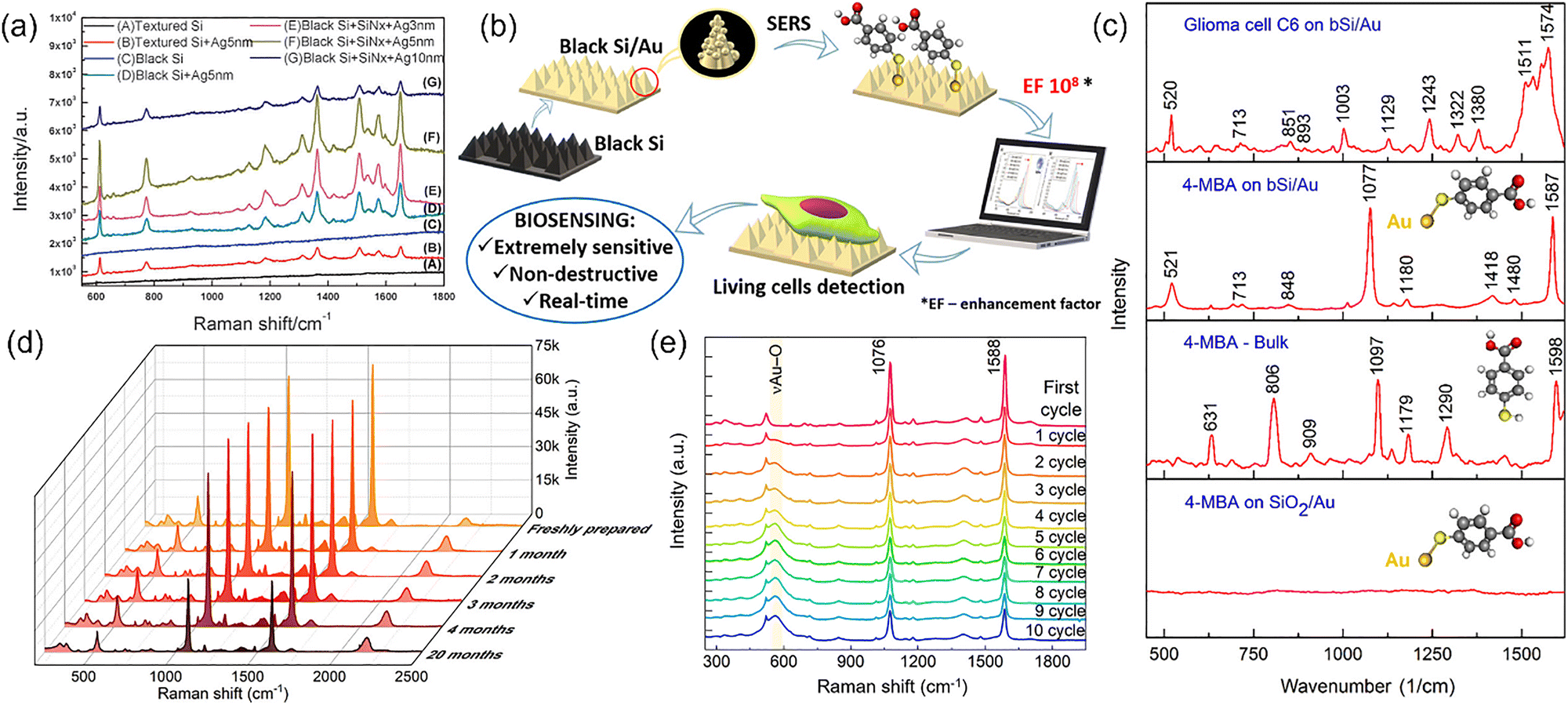 | ||
| Fig. 28 SERS characteristics of black silicon. (a) SERS spectra of Rhodamine 6G recorded on black silicon with different Ag thickness.267 Reproduced with permission from ref. 267. Copyright 2013, Royal Society of Chemistry. (b) Schematic illustration of the SERS process, including structure fabrication, measurement procedures, and applications. (c) Raman spectra of a 4-MBA monolayer on different substrates.51 Reproduced with permission from ref. 51. Copyright 2020, American Chemical Society. (d) Storage stability of the 4-MBA-functionalized black silicon/Au substrate over a period of 20 months. (e) Raman spectra of the substrate after mild oxygen plasma treatment as a surface regeneration process over ten reuse cycles.321 Reproduced with permission from ref. 321. Copyright 2023, American Chemical Society. | ||
4-Mercaptobenzoic acid (4-MBA) is commonly used as a test standard for SERS due to its well-defined self-assembled single-layer structure, with well-known surface density and Raman spectrum. The process of the SERS test is shown in Fig. 28(b). A SERS spectrum of 4-MBA on the black silicon/Au substrate was obtained, as shown in Fig. 28(c).51 The 4-MBA band is not visible on the SiO2/Au substrate but is very clearly observed on the black silicon/Au substrate, with an EF of 2 × 10⁸.
However, the substrate may become contaminated during the testing process, thereby limiting its potential for reuse. According to a study by Golubewa's group,321 as shown in Fig. 28(d), the black silicon/Au substrate exhibited long-term stability when stored in a well-sealed environment. The intensity of the characteristic Raman band decreased by less than 5% after 120 days and by 40% after 20 months. The contaminants on the substrate can be completely removed by treating it with a mild oxygen plasma at room temperature for 35 minutes. The substrate is then rinsed with DI water and dried. After this cleaning process, the substrate can be reused, and the corresponding reuse spectrum is shown in Fig. 28(e). After ten reuse cycles, the Raman signal of 4-MBA molecules covalently bonded to the Au coating is reduced by a factor of four compared with that of the original substrate, indicating good long-term reusability.
Trau et al. designed a digitized nanopillar SERS platform capable of real-time counting of individual cytokines and dynamic monitoring of immune toxicity in patients undergoing immunotherapy.322 The silicon nanopillars were fabricated by RIE, and the SERS nanotags were obtained by modifying the surface of gold–silver alloy nanoboxes with different Raman molecules and corresponding target antibodies. By capturing individual cytokines through discrete pillar arrays, highly specific and sensitive cytokine detection down to the attomolar level can be achieved.
4.6. Bactericidal properties
The nanostructures on black silicon surfaces are well suited for use as antibacterial surfaces and have been widely studied.34,323–325 The application of surface nanostructures for bactericidal and antibiofouling purposes is inspired by the nanocolumn structures on the surface of insect wings,326–328 which can kill bacteria through mechanical action. The physical bactericidal effects of black silicon were reported by Ivanova et al. in 2013.323,329 They compared the bactericidal effect of dragonfly wings with the surface nanostructures of black silicon and concluded that the bactericidal effect was caused by mechanical and structural deformation stress of the surface nanostructures. When bacteria attach to the nanostructured surface, the adhesion force causes the cell membrane to stretch between neighboring nanopillars. Once the stress exceeds a critical threshold, the cell membrane is damaged, resulting in cell death. Remarkably, the antibacterial activity of black silicon surface is comparable to that of natural biologically nanostructured surfaces, such as cicada and dragonfly wings, and it can be further optimized by adjusting the nanostructural parameters.28,330 Even small modifications to the nanostructure can significantly alter its performance as a bactericidal surface. Hence, many researchers have explored the relationship between nanostructural parameters and bactericidal efficacy.325,330–332Ivanova and colleagues fabricated nanopillar arrays on silicon wafers by deep-UV immersion lithography followed by plasma etching.325 The nanoarrays with heights of 220 nm, 360 nm, and 420 nm were prepared by extending the RIE time. They proved that the mechanical cleavage of bacterial cells is related to the elastic restoring force of the nanopillars and the extent of nanopillar clustering. As shown in Fig. 29(a) and (b), bacterial cells appeared collapsed or elongated when trapped between the nanocolumns due to the adhesion force. As the aspect ratio increases, the mechanical energy stored in the columns increases, enhancing the bactericidal effect. However, beyond a certain limit, the nanopillars become more flexible during bacterial interactions and tend to aggregate, forming stable nanopillar bunches with a larger surface area, thereby changing the surface nanostructure and reducing bactericidal efficiency. As the nanopillar height increased, as depicted in Fig. 29(c), the mortality rate of P. aeruginosa cells on black silicon with heights of 220, 360, and 420 nm were 53%, 95%, and 89%, respectively, while those of S. aureus cells were 58%, 83%, and 77%, respectively. Su et al. prepared black silicon microneedles with excellent antimicrobial properties and enhanced drug loading capacity.211 The drug loading efficiency was more than twice that of ordinary silicon microneedles in the same area.
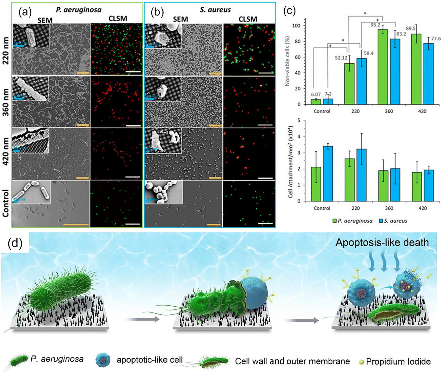 | ||
| Fig. 29 Antibacterial properties of black silicon surfaces. (a) Viability of P. aeruginosa and (b) S. aureus bacterial cells on black silicon samples with different nanostructure heights. (c) Quantification of cell attachment on black silicon.325 Reproduced with permission from ref. 325. Copyright 2020, National Academy of Sciences. (d) Bactericidal mechanism on black silicon, including mechanical injury and apoptosis-like death.34 Reproduced with permission from ref. 34. Copyright 2022, American Chemical Society. | ||
In another research, the authors fabricated a black silicon surface by RIE.330 They found that the bactericidal activity of the nanostructured surface is related to specific parameters such as geometry and surface wettability. When the height of the microcolumn array exceeds 1000 nm, the density is lower than 8 tips per µm2, and the structures are poorly dispersed, the antibacterial performance of the black silicon surface decreases significantly. The nano-morphology parameters of a single surface cannot be directly related to the change of bactericidal activity, but the highest bactericidal efficiency can be achieved by combining different parameters. The exact relationship among these factors is worth investigating deeply.
The synergistic mechanism combining physical and chemical actions has been presented recently.333,334 Zhao et al. posited that mechanical injury alone does not immediately kill bacteria, as the inner plasma membrane often remains intact, allowing some bacteria to survive.34 They explained that an apoptosis-like death is necessary after the initial mechanical injury. Furthermore, they noted that when mechanical stress is removed, damaged cells undergo post-stress apoptosis-like death, which is facilitated by reactive oxygen species (ROS) that accumulate in a non-stressed environment. This indicates that the mechano-bactericidal actions have prolonged physiological impacts on bacteria. According to their findings, illustrated in Fig. 29(d), the sterilization process begins with the mechanical destruction of the bacterial cell wall and outer membrane, followed by a delayed apoptosis-like death, eventually leading to bacterial death through a self-destructive process.
4.7. Biomedical properties
In recent years, black silicon has been increasingly explored in biomedical contexts, not as a chemically functionalized biomaterial, but as a structurally engineered interface capable of interacting with biological systems across multiple length scales. Owing to its intrinsic compatibility with micro–nano fabrication and device integration, black silicon provides a unifying material platform for regulating cell behavior, enabling biosensing and bioimaging, and achieving localized drug delivery. In these applications, the biological performance of black silicon is determined less by its elemental composition and more by how its nanostructured geometry mediates physical interactions with biomolecules, cells, and tissues.At the molecular level, confinement within nanoscale pores and between adjacent nanostructures allows proteins, nucleic acids, enzymes, and small-molecule therapeutics to be immobilized with reduced conformational disruption. The local physical environment provided by porous silicon stabilizes biomolecular structure and enables predictable release behavior governed by diffusion pathways, pore connectivity, and interfacial interactions. As a result, porous silicon functions as an active host matrix that regulates molecular exchange rather than serving as a passive carrier.
Importantly, these nano-bio interfacial effects are highly sensitive to geometric parameters such as pore size distribution, aspect ratio, surface roughness, and structural ordering. Subtle variations in morphology can significantly alter adsorption capacity, release kinetics, and interfacial transport, thereby determining biological performance. This morphology-driven nature of nano-bio interactions establishes structural design as a primary control knob in biomedical applications of black silicon, forming the mechanistic basis for subsequent regulation of cellular responses, sensing, imaging, and drug delivery.
A key consequence of nanostructure geometry is the induction of membrane curvature, which plays a central role in regulating intracellular uptake. Vertically aligned silicon nanowires and nanoneedles impose localized curvature on the plasma membrane, lowering the energetic barrier for membrane wrapping and promoting endocytic pathways. The membrane-wrapping and endocytic internalization process induced by silicon nanostructures is schematically illustrated in Fig. 30(a), with representative confocal fluorescence images showing nanowire internalization in Fig. 30(b). This effect has been directly observed in studies on unlabeled independent silicon nanowires, where spontaneous cellular internalization, active intracellular transport, and eventual perinuclear accumulation were reported, enabling the probing of intracellular biophysical dynamics.338 The efficiency of uptake strongly depends on nanostructure diameter and tip radius, with sharper and smaller features facilitating membrane deformation and enhancing endocytosis.
 | ||
| Fig. 30 Black silicon nanostructures serve as versatile biointerfaces. (a) Schematic illustration of SiNW internalization. (b) Confocal fluorescence micrograph of SiNW internalization (blue scattering).338 Reproduced with permission from ref. 338. Copyright 2016, American Association for the Advancement of Science. (c) Topical delivery behavior of SiNWs.339 Reproduced with permission from ref. 339. Copyright 2024, American Chemical Society. (d) Working principle of silicon nanoneedles for ocular drug delivery. (e) Variation of drug dose with the surface porosity of the nanoneedle array. (f) Variation of drug dose with the length of the nanoneedle array.340 Reproduced with permission from ref. 340. Copyright 2022, American Association for the Advancement of Science. (g) SEM image of 500 µm tall nanoneedles.341 Reproduced with permission from ref. 341. Copyright 2023, Elsevier. | ||
Beyond uptake processes, nanostructured silicon interfaces exert broad influence over cell fate and collective behavior.337 The protruding features of nanoneedle arrays provide abundant anchoring sites for filopodia, enhancing adhesion strength while restricting excessive cell spreading and reducing detachment. During stem cell differentiation, curvature-sensitive membrane proteins can be preferentially localized at these protrusions, promoting protrusive growth and lineage-specific differentiation. Moreover, nanostructure density and spatial arrangement further modulate adhesion, migration, and proliferation: high-density nanoneedle arrays generally reduce effective adhesion area and migration velocity while maintaining or even enhancing proliferation, as revealed by high-content live-cell imaging.339 Conversely, patterned nanostructured silicon surfaces can generate cytophilic and cytophobic regions that guide cell alignment and directional migration,342 demonstrating that geometry alone can act as a physical cue for spatial regulation of cell behavior.
Collectively, these findings demonstrate that cellular behavior on black silicon is tightly coupled to nanoscale morphology. By tailoring nanostructure geometry, porosity, and spatial distribution, black silicon platforms enable precise control over cell-material interfaces, intracellular delivery efficiency, and long-term cellular functions, providing a versatile physical strategy for regulating cell behavior in biomedical applications.
In bio-sensing applications, vertically aligned nanostructures establish tight electrical and mechanical coupling with cells, enabling direct access to intracellular and membrane-associated signals. For example, biomimetic nano-transistor arrays fabricated on nanostructured silicon substrates have demonstrated the ability to simultaneously record electrical activity and mechanical forces at the single-cell level, achieving label-free, sub-millisecond resolution and scalable readout.343 Such platforms demonstrate how nanostructured silicon bridges electrical, mechanical, and biological domains, providing advantages for tracking and distinguishing cell states in drug studies.
Nanostructured silicon platforms have also enabled advanced bio-imaging and molecular analysis by enhancing signal transduction and spatial resolution. Gold nanoparticle-assisted black silicon substrates fabricated via RIE have been successfully applied in surface-assisted laser desorption/ionization mass spectrometry imaging, enabling metabolite mapping from fingerprints and biological tissues with high sensitivity and dual-polarity detection.27 These results demonstrate that black silicon nanostructures can function as efficient interfaces for label-free bio-imaging and chemical mapping at biologically relevant length scales.
In parallel, black silicon-based nanoneedle and microneedle platforms enable localized and minimally invasive drug delivery across multiple biological barriers.344–347 Biodegradable porous silicon nanoneedles embedded in adhesive patches conform closely to the skin of living animals, causing minimal discomfort. They are effective for tissue-level nanoinjection,339 the mechanism is shown in Fig. 30(c), providing uniform, sustained, and localized delivery while maintaining structural integrity. The nanoneedles are fabricated using RIE to define the conical shape, followed by MACE, in which varying the etchant composition allows precise control over the surface porosity of the nanostructures.
Biodegradable silicon nanoneedles integrated with tear-soluble contact lenses have been shown to achieve two-stage ocular drug delivery.340 As shown in Fig. 30(d), when the dissolvable contact lens conforms to the eye, silicon nanoneedles are mechanically inserted into the corneal epithelial layer. The contact lens subsequently dissolves in tear fluid within approximately one minute, triggering immediate drug release, while the residual silicon nanoneedle network degrades slowly, enabling prolonged drug delivery. Standard photolithography and anisotropic DRIE define vertically ordered silicon micropillar arrays, which are then shrunk in 10% KOH at 25 °C for 10 min and further modified by MACE to control surface porosity. For instance, as shown in Fig. 30(e) and (f), immunoglobulins 647 dosage increased from 10.17 ± 0.70 to 17.44 ± 0.74 µg as silicon nanoneedle surface porosity increased from 0 to 60% at a fixed length of 60 µm; similarly, dosage increased from 1.41 ± 0.16 to 13.88 ± 0.14 µg as length increased from 10 to 60 µm at 30% porosity. Hollow silicon microneedle arrays (Fig. 30(g)) fabricated by combined wet and dry etching allow both transdermal drug infusion and interstitial fluid sampling,341 supporting integrated therapeutic and diagnostic functions. These arrays deliver fluids up to several mL at 30 µL min−1 and withdraw 1 µL of interstitial fluid via capillary action.
Collectively, these studies demonstrate that black silicon serves as a versatile and scalable bio-platform in which morphology-engineered nanostructures unify sensing, imaging, and delivery functions. By leveraging the same structural parameters that govern optical and electronic performance, black silicon enables multifunctional biomedical systems capable of interacting with biological environments across molecular, cellular, and tissue length scales.
4.8. Others
Beyond self-cleaning and anti-frosting functionalities, the superhydrophobic nature of black silicon also profoundly affects interfacial fluid dynamics. Specifically, nano/micro hierarchical structures created by DRIE or combined DRIE-MACE processes can modulate the slip behavior at the air–water interface by introducing trapped air pockets that effectively reduce liquid–solid contact. Choi and Kim reported that nanoengineered superhydrophobic surfaces exhibited substantial slip lengths,352 approximately 20 µm for water and 50 µm for 30 wt% glycerin, confirming the critical role of surface morphology in drag reduction and flow enhancement at micro- and nanoscales. Similarly, Lee and Kim demonstrated that microstructured silicon arrays fabricated via DRIE achieved pronounced slip flow behavior,353 which can be attributed to the formation of stable air layers and minimized viscous dissipation at the solid–liquid boundary. These findings highlight the potential of black silicon and DRIE-MACE-derived surfaces not only for superhydrophobicity but also for manipulating interfacial hydrodynamics, offering new strategies for drag reduction and efficient microfluidic transport.
Thermal annealing has been demonstrated to increase the hydrophilicity of planar silicon. As the annealing temperature increases, the static contact angle decreases. However, for black silicon, thermal annealing increases its hydrophobicity, which is attributed to the rough surface with numerous microstructures.354 Annealing optimizes the morphology and chemical composition of black silicon, thereby reducing the contact area and interaction between water droplets and the surface. The hydrophobic property of black silicon can also be used in microfluidic device design,355 which involves fabrication by DRIE through alternating SF6 etching and C4F8 passivation cycles. In this process, black silicon nanostructures are directly formed on the inner surfaces of the silicon microchannel before sealing, as the DRIE step etches the exposed silicon regions defined by the SU-8 or SiO2 hard masks. When liquids in a microfluidic channel converge and merge, bubble encapsulation usually occurs at the point of convergence. Using black silicon on the inner surface of the pipe makes it difficult for liquid in the microchannel to penetrate the nanostructured layer, thus creating a ventilation channel between the liquid sidewalls and preventing the formation of bubbles.
Wang et al. prepared black silicon with various doping levels via femtosecond laser irradiation in SF6 and NF3 mixed gases to study its sensing ability in NO2 gases at room temperature.183 Different responses varied by changing the doping ratio of S and N, as different ratios resulted in different superdoping, and further led to different morphology and defects of black silicon. Higher sulfur content produced sharper and more separated spikes, whereas higher nitrogen content led to blunter features. This method offered high selectivity and yielded a response of approximately 3955% to 20 ppm NO2 when the SF6/NF3 ratio was 56/14. Zhuang et al. fabricated N-hyperdoped NO2 gas sensors and studied the impact of annealing temperature on their performance.184 Low-temperature annealing had minimal influence on the electrical properties of black silicon sensors. With increasing temperature, the resistance first slightly decreased, then increased sharply, and eventually dropped significantly. These changes were attributed to variations in the number of nanoparticles within the microstructure, which altered the surface states of black silicon. At an optimal annealing temperature of 873 K, the sensor achieved a detection limit of 7 ppb and an ultra-wide dynamic range spanning approximately five orders of magnitude.
Following this, Xu et al. prepared black silicon using MACE and applied a polystyrene coating onto its surface to minimize heat loss,360 enabling stable PTE operation. This study further demonstrates that black silicon, with its near-unity broadband absorptance and efficient light-to-heat conversion characteristics, is well-suited for PTE applications.
Additionally, Cheng et al. assessed the photothermal conversion performance of black silicon prepared by RIE.361 They observed that under increased solar irradiation, the surface temperature of both black silicon and bare silicon gradually rose, with the black silicon heating up more quickly and reaching higher temperatures at the same intervals. Zhang's study echoed these findings, further affirming black silicon as a promising material for PTE conversion applications.159 After 1 hour of solar-driven evaporation, the evaporated mass changes for pure water in a Teflon beaker without silicon (control group), water containing disordered nanoporous silicon, and water containing order–disorder hybrid silicon reached 1.35, 2.43, and 2.50 g, respectively. The nanostructured silicon achieved nearly double the water evaporation rate.
4.9. Application-specific morphology of black silicon
Across the applications discussed in this review, the functionality of black silicon is closely linked to its surface morphology, which is ultimately determined by chemistry-driven fabrication processes. High-aspect-ratio nanowires, nanocones, and hierarchical textures are predominantly employed in photodetectors and solar cells to enhance broadband light absorption and suppress surface reflection. Porous and defect-rich morphologies, often generated through chemical etching or MACE, are particularly effective for surface-sensitive applications such as gas sensing, photocatalysis, and SERS, where abundant active sites and enhanced interfacial interactions are required.For THz devices and field emission, sharp-tip or periodically structured morphologies enable strong local electric-field enhancement, facilitating efficient carrier emission and electromagnetic coupling. In contrast, applications involving wettability control and antibacterial activity primarily rely on multiscale roughness and high-aspect-ratio features, which regulate solid–liquid or cell–surface interactions through physical mechanisms. In biomedical-related applications, nanoscale roughness, curvature, and surface states play a decisive role in modulating protein adsorption, cellular responses, and light-matter-biological interactions. Collectively, these observations highlight morphology engineering as a unifying strategy that bridges chemical fabrication routes and the diverse advanced material applications of black silicon. These application-specific morphology–function relationships are systematically summarized in Table 7, which correlates representative black silicon morphologies with their dominant interaction mechanisms and targeted application domains.
| Application | Dominant morphology characteristics | Functional role |
|---|---|---|
| Photodetectors | High-aspect-ratio nanowires/nanocones | Broadband absorption and efficient carrier generation |
| Solar cells | Hierarchical micro–nano textures | Reflection suppression and optical coupling |
| Photocatalysis | Porous, defect-rich structures | Increased active surface and reaction sites |
| Terahertz devices/Field emission | Sharp-tip or periodic nanostructures | Local electric-field enhancement |
| SERS | Nanoscale roughness with hierarchical features | Electromagnetic hot-spot formation |
| Antibacterial surfaces | High-aspect-ratio and mechanically sharp features | Physical disruption of bacterial membranes |
| Gas sensors | Porous or spike-like morphologies | Enhanced adsorption and surface charge transfer |
| PTE conversion | Broadband-absorbing nanostructures | Efficient light-to-thermal or light-to-electric conversion |
| Biomedical applications | Controlled nanoscale roughness and curvature | Regulation of nano-bio interfacial interactions |
5. Emerging directions, challenges, and outlook
The journey from traditional materials to those with micro- and nanostructured surfaces signifies a paradigm shift in materials science and device engineering. As micro- and nanotechnologies continue to advance, the development of materials with precisely engineered micro- and nanostructures—such as nanopillars, nanowires, and porous surfaces—has led to significant improvements in device performance across various domains. These structures, by enhancing the surface area, light absorption, and overall sensitivity, facilitate the realization of highly efficient, compact, and robust devices. Such advancements have profound implications for fields such as optoelectronics, sensors, and energy harvesting.There is no doubt that black silicon holds great promise for the future. With continued scientific research and advancements in the semiconductor industry, its applications are expected to expand even further. The desired performance can be achieved through the precise control of material and process parameters. Despite its numerous advantageous properties, there are still many problems to be solved in its application process. The existing problems and future development trends of black silicon are shown in Fig. 31.
 | ||
| Fig. 31 Outlook and future trend for black silicon. | ||
Mass production challenges
Techniques such as RIE demand low temperatures to reduce surface damage, while the mechanisms of MACE remain partially understood. Furthermore, managing the doping concentration and precision in femtosecond laser irradiation is challenging, and PIIIE shows a rapid decrease in doping concentration with depth. These factors emphasize the need for more research into scalable and controllable production processes.Surface morphology optimization
The nanostructured surface of black silicon, though beneficial for light absorption, creates challenges in carrier transport, recombination, and electrode contact due to the irregularity and gaps between nanostructures. This limits device performance. Therefore, more uniform or novel structures should be investigated for better performance. On the other hand, with the development of new technologies and in-depth research and improvement of existing technologies, more fascinating improvements will appear.Expanding light absorption range
Current methods struggle to extend black silicon's light absorption beyond 1100 nm. Developing advanced methods to broaden this range, especially to achieve high responses at optical communication wavelengths such as 1060, 1330, and 1550 nm, remains a key research goal for enhancing the capabilities of black silicon-based photodetectors.Exploring unique properties
Black silicon's properties, such as near-complete light absorption, enhanced catalytic reactivity, and beneficial surface defects for luminescence (though detrimental for photovoltaic performance), provide vast potential for further exploration. Innovations like exploiting the quantum confinement effect in nanostructured black silicon could lead to new electronic and optical behaviors with tunable band gaps. Integrating metal nanoparticles to induce plasmonic resonance effects could also enhance light–matter interactions, broadening the applications in photovoltaics and beyond. Recent work by Wang et al. has further demonstrated the power of advanced characterization techniques in probing such unique properties, providing valuable insights into spin-dependent transport phenomena in semiconductor materials.362Surface chemical bond engineering
The various surface chemical bonds formed during black silicon fabrication—such as Si–H, Si–O, and Si–F—play a crucial role in determining surface energy, passivation quality, and carrier recombination rates. However, these bonds can also introduce trap states or affect environmental stability, posing challenges for device reliability. Future research should focus on precise control and modification of these chemical terminations through advanced surface treatments or novel passivation techniques. With ongoing technological progress and a deeper understanding of surface chemistry, significant improvements in electronic and optoelectronic performance are anticipated.Surface defects and passivation techniques
Surface defects significantly impair black silicon's device performance by causing recombination and reducing carrier lifetimes. Developing advanced passivation techniques using materials like SiNx, Al2O3, or organic passivants is crucial. Additionally, new technologies that effectively utilize surface defects could revolutionize black silicon's applications,287 such as alternating current photovoltaic (AC PV) effect.Contact optimization
Despite progress in passivation technologies, achieving efficient electrical contact between black silicon's nanostructured surfaces and electrodes remains difficult. This limitation restricts performance enhancement, especially in devices with nanostructured surfaces. Enhancing contact design and integration is vital for unlocking the full potential of black silicon devices.Uniform morphology for scalability
Achieving uniform nanostructures remains a key challenge for large-scale production and performance consistency, and ancillary processes such as photolithography and masks are commonly used to form ordered micro–nanostructures. The inhomogeneity of current fabrication methods leads to variations in optical and electrical properties, limiting the reliability and scalability of black silicon applications. The development of fabrication processes that ensure morphological homogeneity is critical for the widespread use of black silicon in commercial devices.Specialized applications
Black silicon has shown potential in a wide range of applications, from infrared detectors to solar cells to antimicrobial surfaces. However, further research is needed to explore its potential in specialized applications, such as biomedicine and advanced sensing technologies. By leveraging its unique properties, black silicon could become a key material for next-generation devices.Biological research
The biological applications of black silicon, such as its bactericidal properties and potential in drug delivery, remain underexplored. Future research should focus on understanding the relationship between its nanostructures and biological effects, promoting its integration into biomedical fields.The journey of black silicon from a niche material to a mainstream technology hinges on overcoming these challenges. By addressing production scalability, enhancing surface properties, and leveraging its unique optoelectronic and biological characteristics, black silicon can play a pivotal role in next-generation device technologies.
Author contributions
Junling Lv: writing – original draft, writing – reviewing & editing, investigation, visualization; Lihong Jiang: visualization, investigation; Xinlin Liu: methodology; Gaojie Li: visualization; Mingrui Qian: visualization, investigation; Mingxin Tang: methodology; Xinao Cheng: investigation; Lan Lu: investigation; Xiarong Ren: investigation; Xueling Zhang: investigation; Haiyang Zou: conceptualization, original draft, project administration, resources, funding acquisition, writing – reviewing and editing, supervision; Zhong Lin Wang: conceptualization, writing – reviewing and editing, supervision.Conflicts of interest
There are no conflicts to declare.Data availability
No primary research results, software or code have been included, and no new data were generated or analyzed as part of this review.Acknowledgements
This work was supported by National Natural Science Foundation of China (Grant No. 52573253), the Fundamental Research Funds for the Central Universities (YJ202293), the TCL Science and Technology Innovation Fund, and the Distinguished Young Scholars of the National Natural Science Foundation of China (Overseas) (00301054A1091), Beijing Key Laboratory of High-Entropy Energy Materials and Devices, Beijing Institute of Nanoenergy and Nanosystems (No. GS2025ZD010).References
- Y. Li, C. Liu, H. Zou, L. Che, P. Sun, J. Yan, W. Liu, Z. Xu, W. Yang, L. Dong, L. Zhao, X. Wang, G. Wang and Z. L. Wang, Cell Rep. Phys. Sci., 2023, 4, 101191 CrossRef.
- S. Gupta, A. Knoepfel, H. Zou and Y. Ding, Sens. Actuators, B, 2023, 392, 134030 CrossRef CAS.
- H. Zou, L. Guo, H. Xue, Y. Zhang, X. Shen, X. Liu, P. Wang, X. He, G. Dai, P. Jiang, H. Zheng, B. Zhang, C. Xu and Z. L. Wang, Nat. Commun., 2020, 11, 2093 CrossRef CAS PubMed.
- P. K. Bondyopadhyay, Proc. IEEE, 1998, 86, 78–81 CrossRef.
- W. Yangyuan, H. Ruqi, L. Xiaoyan and K. Jinfeng, Beijing, China, 1998.
- S. Zeng, C. Liu and P. Zhou, Nat. Rev. Electr. Eng., 2024, 1, 335–348 CrossRef.
- Y. Zhang and G. Chen, Light: Sci. Appl., 2024, 13, 87 CrossRef CAS PubMed.
- X. Liu, P. R. Coxon, M. Peters, B. Hoex, J. M. Cole and D. J. Fray, Energy Environ. Sci., 2014, 7, 3223–3263 RSC.
- J. Lv, T. Zhang, P. Zhang, Y. Zhao and S. Li, Nanoscale Res. Lett., 2018, 13, 1–10 CrossRef PubMed.
- Z. Zhao, Z. Zhang, J. Jing, R. Gao, Z. Liao, W. Zhang, G. Liu, Y. Wang, K. Wang and C. Xue, APL Mater., 2023, 11, 021107 CrossRef CAS.
- A. J. Bett, J. Eisenlohr, O. Höhn, P. Repo, H. Savin, B. Bläsi and J. C. Goldschmidt, Opt. Express, 2016, 24, A434–A445 CrossRef CAS PubMed.
- S. Uddin, M. R. Hashim and M. Z. Pakhuruddin, Opt. Mater., 2022, 134, 113111 CrossRef CAS.
- J. Yang, F. Luo, T. S. Kao, X. Li, G. W. Ho, J. Teng, X. Luo and M. Hong, Light: Sci. Appl., 2014, 3, e185 CrossRef CAS.
- L. Meng, M. Awashra, S. M. Mirmohammadi, S. M. Mousavi, J. Vapaavuori, V. P. Jokinen and S. Franssila, Nanoscale, 2025, 17, 2871–2877 RSC.
- Y. He, C. Jiang, H. Yin, J. Chen and W. Yuan, J. Colloid Interface Sci., 2011, 364, 219–229 CrossRef CAS PubMed.
- Z. Fekete, Á. C. Horváth, Z. Bérces and A. Pongrácz, Sens. Actuators, A, 2014, 216, 277–286 CrossRef CAS.
- Y. Yu, Z. Zhang, X. Yin, A. Kvit, Q. Liao, Z. Kang, X. Yan, Y. Zhang and X. Wang, Nat. Energy, 2017, 2, 17045 CrossRef CAS.
- E. Mitsai, A. Kuchmizhak, E. Pustovalov, A. Sergeev, A. Mironenko, S. Bratskaya, D. P. Linklater, A. Balčytis, E. Ivanova and S. Juodkazis, Nanoscale, 2018, 10, 9780–9787 RSC.
- Y. Yang, Z.-Y. Ren, C. Li and J.-H. Zhao, Opt. Quantum Electron., 2023, 55, 259 CrossRef CAS.
- S. Huang, G. Deng, X. Jin, Y. Lu, G. Song, H. Huang, P. Zhao, C. Zhang, J. Yao, Q. Wu and J. Xu, Opt. Mater., 2020, 110, 110474 CrossRef CAS.
- A. Alsolami, H. Hussain, R. Noor, N. AlAdi, N. Almalki, A. Kurdi, T. Tabbakh, A. Zaman, S. Alfihed and J. Wang, Appl. Sci., 2024, 14, 9841 CrossRef CAS.
- Y. Xia, B. Liu, J. Liu, Z. Shen and C. Li, Sol. Energy, 2011, 85, 1574–1578 CrossRef CAS.
- H. Savin, P. Repo, G. von Gastrow, P. Ortega, E. Calle, M. Garín and R. Alcubilla, Nat. Nanotechnol., 2015, 10, 624–628 CrossRef CAS PubMed.
- G. Seniutinas, G. Gervinskas, R. Verma, B. D. Gupta, F. Lapierre, P. R. Stoddart, F. Clark, S. L. McArthur and S. Juodkazis, Opt. Express, 2015, 23, 6763–6772 CrossRef CAS PubMed.
- Y. Zhao, X.-L. Liu, S.-X. Ma, W.-J. Wang, X.-J. Ning, L. Zhao and J. Zhuang, Sens. Actuators, B, 2021, 340, 129985 CrossRef CAS.
- M. Aleem, R. Vishnuraj and B. Pullithadathil, RSC Appl. Interfaces, 2025, 2, 220–229 RSC.
- S. A. Iakab, P. Ràfols, M. Tajes, X. Correig-Blanchar and M. García-Altares, ACS Nano, 2020, 14, 6785–6794 CrossRef CAS PubMed.
- F. Tian, M. Li, S. Wu, L. Li and H. Hu, Colloids Surf., B, 2023, 222, 113092 CrossRef CAS PubMed.
- Y. Wang, Y. Yang, Y. Shi, H. Song and C. Yu, Adv. Mater., 2020, 32, 1904106 CrossRef CAS PubMed.
- D. H. K. Nguyen, V. T. H. Pham, M. Al Kobaisi, C. Bhadra, A. Orlowska, S. Ghanaati, B. M. Manzi, V. A. Baulin, S. Joudkazis, P. Kingshott, R. J. Crawford and E. P. Ivanova, Langmuir, 2016, 32, 10744–10751 CrossRef CAS PubMed.
- D. P. Linklater, S. Juodkazis, S. Rubanov and E. P. Ivanova, ACS Appl. Mater. Interfaces, 2017, 9, 29387–29393 CrossRef CAS PubMed.
- W. Xu, C. Pang, C. Song, J. Qian, S. Feola, V. Cerullo, L. Fan, H. Yu and V.-P. Lehto, Acta Biomater., 2022, 152, 473–483 CrossRef CAS PubMed.
- C. Nataraj, K. Mohanta and G. P. Badhirappan, J. Mater. Chem. C, 2025, 13, 5868–5879 RSC.
- S. Zhao, Z. Li, D. P. Linklater, L. Han, P. Jin, L. Wen, C. Chen, D. Xing, N. Ren, K. Sun, S. Juodkazis, E. P. Ivanova and L. Jiang, Nano Lett., 2022, 22, 1129–1137 CrossRef CAS PubMed.
- Y.-L. Deng and Y.-J. Juang, Biosens. Bioelectron., 2014, 53, 37–42 CrossRef CAS PubMed.
- Z. Fan, D. F. Cui, Z. X. Zhang, Z. Zhao, H. M. Chen, Y. Y. Fan, P. L. Li, Z. D. Zhang, C. Y. Xue and S. B. Yan, Nanomaterials, 2021, 11, 41 CrossRef CAS PubMed.
- Z. Huang, N. Geyer, P. Werner, J. de Boor and U. Gösele, Adv. Mater., 2011, 23, 285–308 CrossRef CAS PubMed.
- C. Huo, J. Wang, H. Fu, X. Li, Y. Yang, H. Wang, A. Mateen, G. Farid and K.-Q. Peng, Adv. Funct. Mater., 2020, 30, 2005744 CrossRef CAS.
- J. H. Zhao, X. B. Li, Q. D. Chen, Z. G. Chen and H. B. Sun, Mater. Today Nano, 2020, 11, 100078 CrossRef.
- A. Kumar, M. Devi, M. Kumar, A. Shrivastava, R. Sharma, T. Dixit, V. Singh, K. Shehzad, Y. Xu, K. Singh and H. Hu, Sens. Actuators, A, 2022, 347, 113912 CrossRef CAS.
- M. Otto, M. Algasinger, H. Branz, B. Gesemann, T. Gimpel, K. Füchsel, T. Käsebier, S. Kontermann, S. Koynov, X. Li, V. Naumann, J. Oh, A. N. Sprafke, J. Ziegler, M. Zilk and R. B. Wehrspohn, Adv. Opt. Mater., 2015, 3, 147–164 CrossRef CAS.
- L. Chen, S. Zhang, Y. Duan, X. Song, M. Chang, W. Feng and Y. Chen, Chem. Soc. Rev., 2024, 53, 1167–1315 RSC.
- S. A. Ahad, T. Kennedy and H. Geaney, ACS Energy Lett., 2024, 9, 1548–1561 CrossRef CAS PubMed.
- S. Wei, X. Xia, S. Bi, S. Hu, X. Wu, H.-Y. Hsu, X. Zou, K. Huang, D. W. Zhang, Q. Sun, A. J. Bard, E. T. Yu and L. Ji, Chem. Soc. Rev., 2024, 53, 6860–6916 RSC.
- J. H. Zhao, C. H. Li, X. B. Li, Q. D. Chen, Z. G. Chen and H. B. Sun, IEEE Trans. Electron Devices, 2018, 65, 4905–4909 CAS.
- X. Zhou, L. Wan, H. Li, X. Yang, J. Chen, K. Ge, J. Yan, C. Zhang, Q. Gao, X. Zhang, J. Guo, F. Li, J. Wang, D. Song, S. Wang, B. S. Flavel and J. Chen, Small, 2023, 19, 2205848 CrossRef CAS PubMed.
- R. Komatsu, A. Balčytis, G. Seniutinas, T. Yamamura, Y. Nishijima and S. Juodkazis, Sol. Energy Mater. Sol. Cells, 2015, 143, 72–77 CrossRef CAS.
- C. Ramos, Y. Verduzco-López, C. Álvarez-Macías, A. Sanchez-Juarez, A. Dutt and G. Santana, Mater. Today Commun., 2019, 20, 100556 CrossRef CAS.
- M. Ali, F. Zhou, K. Chen, C. Kotzur, C. Xiao, L. Bourgeois, X. Zhang and D. R. MacFarlane, Nat. Commun., 2016, 7, 11335 CrossRef CAS PubMed.
- P. Hoyer, M. Theuer, R. Beigang and E.-B. Kley, Appl. Phys. Lett., 2008, 93, 091106 CrossRef.
- L. Golubewa, R. Karpicz, I. Matulaitiene, A. Selskis, D. Rutkauskas, A. Pushkarchuk, T. Khlopina, D. Michels, D. Lyakhov, T. Kulahava, A. Shah, Y. Svirko and P. Kuzhir, ACS Appl. Mater. Interfaces, 2020, 12, 50971–50984 CrossRef CAS PubMed.
- H. Robbins and B. Schwartz, J. Electrochem. Soc., 1959, 106, 505 CrossRef CAS.
- H. Jansen, M. d Boer, R. Legtenberg and M. Elwenspoek, J. Micromech. Microeng., 1995, 5, 115 CrossRef CAS.
- D. Dimova-Malinovska, M. Sendova-Vassileva, N. Tzenov and M. Kamenova, Thin Solid Films, 1997, 297, 9–12 CrossRef CAS.
- T.-H. Her, R. J. Finlay, C. Wu, S. Deliwala and E. Mazur, Appl. Phys. Lett., 1998, 73, 1673–1675 CrossRef CAS.
- R. Memming and G. Schwandt, Surf. Sci., 1966, 4, 109–124 CrossRef CAS.
- N. W. Cheung, Mater. Chem. Phys., 1996, 46, 132–139 CrossRef CAS.
- C. Wu, C. H. Crouch, L. Zhao, J. E. Carey, R. Younkin, J. A. Levinson, E. Mazur, R. M. Farrell, P. Gothoskar and A. Karger, Appl. Phys. Lett., 2001, 78, 1850–1852 CrossRef CAS.
- K. Yasuda, T. Nohira, K. Amezawa, Y. H. Ogata and Y. Ito, J. Electrochem. Soc., 2005, 152, D69 CrossRef CAS.
- B. Franta, D. Pastor, H. H. Gandhi, P. H. Rekemeyer, S. Gradečak, M. J. Aziz and E. Mazur, J. Appl. Phys., 2015, 118, 225303 CrossRef.
- L. L. Janavicius, J. A. Michaels, C. Chan, D. J. Sievers and X. Li, Appl. Phys. Rev., 2023, 10, 011409 CAS.
- A. Uhlir, Bell Syst. Tech. J., 1956, 35, 333–347 CrossRef CAS.
- Y. Bi, X. Su, S. Zou, Y. Xin, Z. Dai, J. Huang, X. Wang and L. Zhang, Thin Solid Films, 2012, 521, 176–180 Search PubMed.
- K. N. Nguyen, P. Basset, F. Marty, Y. Leprince-Wang and T. Bourouina, J. Appl. Phys., 2013, 113, 194903 Search PubMed.
- Z. Zhang, T. Martinsen, G. Liu, M. Tayyib, D. Cui, M. J. de Boer, F. Karlsen, H. Jakobsen, C. Xue and K. Wang, Adv. Opt. Mater., 2020, 8, 2000668 Search PubMed.
- D. Schmelz, T. Käsebier, Z. Shi, Q. Cheng, N. Sergeev, D. Schelle and U. Zeitner, Mater. Sci. Semicond. Process., 2023, 165, 107646 CrossRef CAS.
- S. Sarkar, A. A. Elsayed, Y. M. Sabry, F. Marty, J. Drévillon, X. Liu, Z. Liang, E. Richalot, P. Basset, E. Nefzaoui and T. Bourouina, Adv. Photonics Res., 2023, 4, 2200223 CrossRef CAS.
- X. Li and P. W. Bohn, Appl. Phys. Lett., 2000, 77, 2572–2574 Search PubMed.
- S. Koynov, M. S. Brandt and M. Stutzmann, Appl. Phys. Lett., 2006, 88, 203107 CrossRef.
- J. Q. Huang, S. Y. Chiam, H. H. Tan, S. J. Wang and W. K. Chim, Chem. Mater., 2010, 22, 4111–4116 CrossRef CAS.
- N. A. Md Noor, S. K. Mohamad, S. S. Hamil, M. Devarajan and M. Z. Pakhuruddin, Mater. Sci. Semicond. Process., 2019, 91, 167–173 CrossRef.
- R. Younkin, J. E. Carey, E. Mazur, J. A. Levinson and C. M. Friend, J. Appl. Phys., 2003, 93, 2626–2629 CrossRef CAS.
- M. Sheehy, L. Winston, J. Carey, C. Friend and E. Mazur, Chem. Mater., 2005, 17, 3582–3586 CrossRef CAS.
- B. R. Tull, J. E. Carey, E. Mazur, J. P. McDonald and S. M. Yalisove, MRS Bull., 2006, 31, 626–633 CrossRef CAS.
- Y. Ma, J. Si, X. Sun, T. Chen and X. Hou, Appl. Surf. Sci., 2014, 313, 905–910 CrossRef CAS.
- Z. X. Jia, Q. Wu, X. R. Jin, S. Huang, J. Z. Li, M. Yang, H. Huang, J. H. Yao and J. J. Xu, Opt. Express, 2020, 28, 5239–5247 CrossRef PubMed.
- A. Y. Vorobyev and C. Guo, Appl. Surf. Sci., 2011, 257, 7291–7294 CrossRef CAS.
- M. Kovalev, I. Podlesnykh, A. Nastulyavichus, N. Stsepuro, I. Mushkarina, P. Platonov, E. Terukov, S. Abolmasov, A. Dunaev, A. Akhmatkhanov, V. Shur and S. Kudryashov, Materials, 2023, 16, 2350 CrossRef CAS PubMed.
- X. Liu, B. Radfar, K. Chen, E. Pälikkö, T. P. Pasanen, V. Vähänissi and H. Savin, IEEE Photonics Technol. Lett., 2022, 34, 870–873 CAS.
- Y. Xia, B. Liu, S. Zhong and C. Li, J. Electron Spectrosc. Relat. Phenom., 2012, 184, 589–592 CrossRef CAS.
- S. Zhong, B. Liu, Y. Xia, J. Liu, J. Liu, Z. Shen, Z. Xu and C. Li, Sol. Energy Mater. Sol. Cells, 2013, 108, 200–204 CrossRef CAS.
- J. W. M. Lim, S. Huang, L. Xu, Y. Y. Lim, Y. X. Loh, C. S. Chan, K. Bazaka, I. Levchenko and S. Xu, Sol. Energy, 2018, 171, 841–850 CrossRef CAS.
- Y. H. Liu, X. K. Wang, J. B. Luo and X. C. Lu, Appl. Surf. Sci., 2009, 255, 9430–9438 CrossRef CAS.
- M. Y. Arafat, M. A. Islam, A. W. B. Mahmood, F. Abdullah, T. S. Kiong and N. Amin, Crystals, 2021, 11, 881 CrossRef CAS.
- X. Y. Ao, X. L. Tong, D. S. Kim, L. B. Zhang, M. Knez, F. Müller, S. L. He and V. Schmidt, Appl. Phys. Lett., 2012, 101, 111901 CrossRef.
- W. Chen, Y. Liu, L. Yang, J. Wu, Q. Chen, Y. Zhao, Y. Wang and X. Du, Sci. Rep., 2018, 8, 3408 CrossRef PubMed.
- E. Vazsonyi, K. De Clercq, R. Einhaus, E. Van Kerschaver, K. Said, J. Poortmans, J. Szlufcik and J. Nijs, Sol. Energy Mater. Sol. Cells, 1999, 57, 179–188 CrossRef CAS.
- R. Liu, J. Wang, T. Sun, M. Wang, C. Wu, H. Zou, T. Song, X. Zhang, S.-T. Lee, Z. L. Wang and B. Sun, Nano Lett., 2017, 17, 4240–4247 CrossRef CAS PubMed.
- M. Kopani, M. Mikula, D. Kosnac, P. Vojtek, J. Gregus, E. Vavrinsky, M. Jergel and E. Pincik, Appl. Surf. Sci., 2018, 461, 44–47 CrossRef CAS.
- J. Müllerová, Ľ. Scholtz, J. Ďurišová, E. Pinčík, M. Solanská and D. Pudiš, Appl. Surf. Sci., 2018, 461, 182–189 CrossRef.
- X. G. Zhang, S. D. Collins and R. L. Smith, J. Electrochem. Soc., 1989, 136, 1561 CrossRef CAS.
- T. Jiang, X. Xu and G. Z. Chen, J. Energy Chem., 2020, 47, 46–61 CrossRef.
- P. R. Coxon, M. Coto, E. Juzeliunas and D. J. Fray, Prog. Nat. Sci.: Mater. Int., 2015, 25, 583–590 CrossRef CAS.
- M. M. Plakhotnyuk, M. Gaudig, R. S. Davidsen, J. M. Lindhard, J. Hirsch, D. Lausch, M. S. Schmidt, E. Stamate and O. Hansen, J. Appl. Phys., 2017, 122, 143101 CrossRef.
- M. Steglich, T. Käsebier, M. Zilk, T. Pertsch, E.-B. Kley and A. Tünnermann, J. Appl. Phys., 2014, 116, 173503 CrossRef.
- J. Xu, A. D. Refino, A. Delvallée, S. Seibert, C. Schwalb, P. E. Hansen, M. Foldyna, L. Siaudinyte, G. Hamdana, H. S. Wasisto, J. Kottmeier, A. Dietzel, T. Weimann, J. K. Prüssing, H. Bracht and E. Peiner, Appl. Phys. Rev., 2024, 11, 021411 CAS.
- A. D. Refino, N. Yulianto, I. Syamsu, A. P. Nugroho, N. H. Hawari, A. Syring, E. Kartini, F. Iskandar, T. Voss, A. Sumboja, E. Peiner and H. S. Wasisto, Sci. Rep., 2021, 11, 19779 CrossRef CAS PubMed.
- N. Lim, Y. Pak, J. T. Kim, Y. Hwang, R. Lee, Y. Kumaresan, N. Myoung, H. C. Ko and G. Y. Jung, Nanoscale, 2015, 7, 13489–13494 RSC.
- S. Wu, Q. Chen, L. Zhang, H. Ren, H. Zhou, L. Hu and C. S. Tan, Nanoscale, 2023, 15, 4843–4851 RSC.
- V. R. Manfrinato, F. E. Camino, A. Stein, L. Zhang, M. Lu, E. A. Stach and C. T. Black, Adv. Funct. Mater., 2019, 29, 1903429 CrossRef CAS.
- S. Kim, G. S. Jeong, N. Y. Park and J.-Y. Choi, Micromachines, 2021, 12, 119 CrossRef PubMed.
- Z. P. Li, Z. M. Xu, X. P. Qu, S. B. Wang, J. Peng and L. H. Mei, Nanotechnology, 2017, 28, 095301 CrossRef CAS PubMed.
- M. Jung, J.-H. Kim and Y.-W. Choi, J. Nanomater., 2018, 2018, 6249890 Search PubMed.
- R. Xu, Z. Zeng and Y. Lei, Nat. Commun., 2022, 13, 2435 CrossRef CAS PubMed.
- H. Zhong, N. Ilyas, Y. Song, W. Li and Y. Jiang, Nanoscale Res. Lett., 2018, 13, 316 CrossRef PubMed.
- F. Laermer and A. Urban, Plasma Processes Polym., 2019, 16, 1800207 CrossRef.
- Z. Zhang, G. Liu and K. Wang, Micromachines, 2021, 12, 1009 CrossRef PubMed.
- E. Vassallo, M. Pedroni, S. M. Pietralunga, R. Caniello, A. Cremona, F. Di Fonzo, F. Ghezzi, F. Inzoli, G. Monteleone, G. Nava, V. Spampinato, A. Tagliaferri, M. Zani and G. Angella, Thin Solid Films, 2016, 603, 173–179 CrossRef CAS.
- F. Ghezzi, M. Pedroni, J. Kovač, F. Causa, A. Cremona, M. Anderle, R. Caniello, S. M. Pietralunga and E. Vassallo, ACS Omega, 2022, 7, 25600–25612 CrossRef CAS PubMed.
- H. M. Branz, V. E. Yost, S. Ward, K. M. Jones, B. To and P. Stradins, Appl. Phys. Lett., 2009, 94, 231121 CrossRef.
- H. Zhong, A. Guo, G. Guo, W. Li and Y. Jiang, Nanoscale Res. Lett., 2016, 11, 322 CrossRef CAS PubMed.
- S. Surdo and G. Barillaro, Small, 2024, 20, 2400499 CrossRef CAS PubMed.
- C.-Y. Chen and C.-P. Wong, Nanoscale, 2015, 7, 1216–1223 RSC.
- G. B. Jung, Y. J. Cho, Y. Myung, H. S. Kim, Y. S. Seo, J. Park and C. Kang, Opt. Express, 2010, 18, 16353–16359 CrossRef CAS PubMed.
- Y. Jeong, C. Hong, Y. H. Jung, R. Akter, H. Yoon and I. Yoon, Sci. Rep., 2019, 9, 15914 CrossRef PubMed.
- J. Soueiti, R. Sarieddine, H. Kadiri, A. Alhussein, G. Lerondel and R. Habchi, Nanoscale, 2023, 15, 4738–4761 RSC.
- X. Geng, M. Li, L. Zhao and P. W. Bohn, J. Electron. Mater., 2011, 40, 2480–2485 CrossRef CAS.
- K. Nishioka, T. Sueto and N. Saito, Appl. Surf. Sci., 2009, 255, 9504–9507 CrossRef CAS.
- K. Peng, M. Zhang, A. Lu, N.-B. Wong, R. Zhang and S.-T. Lee, Appl. Phys. Lett., 2007, 90, 163123 CrossRef.
- M. O. Williams, D. Hiller, T. Bergfeldt and M. Zacharias, J. Phys. Chem. C, 2017, 121, 9296–9299 CrossRef CAS.
- A. Mallavarapu, P. Ajay, C. Barrera and S. V. Sreenivasan, ACS Appl. Mater. Interfaces, 2021, 13, 1169–1177 CrossRef CAS PubMed.
- P. Zhang, S. Li, C. Liu, X. Wei, Z. Wu, Y. Jiang and Z. Chen, Nanoscale Res. Lett., 2014, 9, 519 CrossRef PubMed.
- S. Uddin, M. R. Hashim and M. Z. Pakhuruddin, Mater. Sci. Semicond. Process., 2021, 133, 105932 CrossRef CAS.
- M. Li, Y. Li, W. Liu, L. Yue, R. Li, Y. Luo, M. Trevor, B. Jiang, F. Bai, P. Fu, Y. Zhao, C. Shen and J. M. Mbengue, Mater. Res. Bull., 2016, 76, 436–449 CrossRef CAS.
- J.-J. Huang, C.-S. Huang, J.-Y. Wang, P.-Y. Chang, C.-N. Chen and S.-L. Ou, Appl. Phys. A, 2022, 128, 485 CrossRef CAS.
- S. Ray, A. Mondal and U. Gangopadhyay, Appl. Phys. A, 2020, 126, 399 CrossRef CAS.
- Z. Huang, H. Fang and J. Zhu, Adv. Mater., 2007, 19, 744–748 CrossRef CAS.
- C. Song, B. Ye, J. Xu, J. Chen, W. Shi, C. Yu, C. An, J. Zhu and W. Zhang, Small, 2022, 18, 2104202 CrossRef CAS PubMed.
- F. J. Wendisch, M. Rey, N. Vogel and G. R. Bourret, Chem. Mater., 2020, 32, 9425–9434 CrossRef CAS PubMed.
- D. Brodoceanu, R. Elnathan, B. Prieto-Simón, B. Delalat, T. Guinan, E. Kroner, N. H. Voelcker and T. Kraus, ACS Appl. Mater. Interfaces, 2015, 7, 1160–1169 CrossRef CAS PubMed.
- Y. Chen, C. Zhang, L. Li, C.-C. Tuan, F. Wu, X. Chen, J. Gao, Y. Ding and C.-P. Wong, Nano Lett., 2017, 17, 4304–4310 CrossRef CAS PubMed.
- O. J. Hildreth, A. G. Fedorov and C. P. Wong, ACS Nano, 2012, 6, 10004–10012 CrossRef CAS PubMed.
- O. J. Hildreth and D. R. Schmidt, Adv. Funct. Mater., 2014, 24, 3827–3833 CrossRef CAS.
- X. Zhang, Y. Liu, C. Yao, J. Niu, H. Li and C. Xie, Nanoscale Adv., 2023, 5, 142–152 RSC.
- D. A. Zuev, O. A. Novodvorsky, E. V. Khaydukov, O. D. Khramova, A. A. Lotin, L. S. Parshina, V. V. Rocheva, V. Y. Panchenko, V. V. Dvorkin, A. Y. Poroykov, G. G. Untila, A. B. Chebotareva, T. N. Kost and M. A. Timofeyev, Appl. Phys. B, 2011, 105, 545–550 CrossRef CAS.
- X. Y. Yu, Z. H. Lv, C. H. Li, X. Han and J. H. Zhao, IEEE Sens. J., 2016, 16, 5227–5231 CAS.
- H. Huang, L. M. Yang and J. Liu, Opt. Eng., 2014, 53, 051513 CrossRef.
- S. K. Sundaram and E. Mazur, Nat. Mater., 2002, 1, 217–224 CrossRef CAS PubMed.
- K. C. Phillips, H. H. Gandhi, E. Mazur and S. K. Sundaram, Adv. Opt. Photonics, 2015, 7, 684–712 CrossRef CAS.
- C. H. Crouch, J. E. Carey, J. M. Warrender, M. J. Aziz, E. Mazur and F. Y. Génin, Appl. Phys. Lett., 2004, 84, 1850–1852 CrossRef CAS.
- M.-J. Sher, N. M. Mangan, M. J. Smith, Y.-T. Lin, S. Marbach, T. M. Schneider, S. Gradečak, M. P. Brenner and E. Mazur, J. Appl. Phys., 2015, 117, 125301 CrossRef.
- Y. Ma, H. Ren, J. Si, X. Sun, H. Shi, T. Chen, F. Chen and X. Hou, Appl. Surf. Sci., 2012, 261, 722–726 CrossRef CAS.
- T. Gimpel, S. Winter, M. Boßmeyer and W. Schade, Sol. Energy Mater. Sol. Cells, 2018, 180, 168–172 CrossRef CAS.
- J. Meng, H. Song, X. Li and S. Liu, Appl. Phys. A, 2015, 118, 1197–1203 CrossRef CAS.
- J. Meng, H. Song, X. Li and S. Liu, J. Laser Appl., 2015, 28, 012005 CrossRef.
- H. Mei, C. Wang, J. Yao, Y.-C. Chang, J. Cheng, Y. Zhu, S. Yin and C. Luo, Opt. Commun., 2011, 284, 1072–1075 CrossRef CAS.
- S. Sarkar, E. Nefzaoui, G. Hamaoui, F. Marty, P. Basset and T. Bourouina, Appl. Phys. Lett., 2022, 121, 231703 CrossRef CAS.
- S. Qin, M. I. Current, S. B. Felch, N. W. Cheung and J. Ziegler, Ion Implantation Applications, Science and Technology, 2012, 15, pp. 2–41 Search PubMed.
- X. Liu, B. Radfar, K. Chen, O. E. Setälä, T. P. Pasanen, M. Yli-Koski, H. Savin and V. Vähänissi, IEEE Trans. Semicond. Manuf., 2022, 35, 504–510 Search PubMed.
- X. Tan, Z. Tao, M. Yu, H. Wu and H. Li, Sci. Rep., 2018, 8, 7863 CrossRef PubMed.
- W. Meng, H. Zhong, W. Hou, Y. Gou, Y. Song and W. Li, IOP Conf. Ser.: Mater. Sci. Eng., 2017, 250, 012015 Search PubMed.
- S. Zhou, H. Fan, S. Wen, R. Zhang, Y. Yin, C. Lan, C. Li and Y. Liu, Adv. Opt. Mater., 2024, 12, 2301982 CrossRef CAS.
- P. Yu, J. Wu, S. Liu, J. Xiong, C. Jagadish and Z. M. Wang, Nano Today, 2016, 11, 704–737 CrossRef CAS.
- J. Oh, T. G. Deutsch, H.-C. Yuan and H. M. Branz, Energy Environ. Sci., 2011, 4, 1690–1694 RSC.
- S.-X. Zhang, J.-C. Wang, Y.-M. Zhao, Y.-L. Han, A.-J. Ming, F. Wei and C.-H. Mao, Rare Met., 2023, 42, 2447–2456 CrossRef CAS.
- X. Wang, B. Zhao, J. Nivas, X. Zhao, W. Du and S. Amoruso, Opt. Express, 2024, 32, 36362–36380 CrossRef CAS PubMed.
- J.-X. Wang, B. Cui, C. Salmean, X. Chen, X. Yan, Y. Mao and S. Yao, Nano Energy, 2024, 125, 109560 CrossRef CAS.
- C. Yao, Y. Liu, J. Niu, C. Lu, H. Li and C. Xie, Appl. Surf. Sci., 2024, 655, 159641 CrossRef CAS.
- Z. Zhang, Y. Wang, P. A. Stensby Hansen, K. Du, K. R. Gustavsen, G. Liu, F. Karlsen, O. Nilsen, C. Xue and K. Wang, Nano Energy, 2019, 65, 103992 CrossRef CAS.
- A. Rahman, A. Ashraf, H. Xin, X. Tong, P. Sutter, M. D. Eisaman and C. T. Black, Nat. Commun., 2015, 6, 5963 CrossRef CAS PubMed.
- U. K. Mishra and J. Singh, Semiconductor device physics and design, Springer, 2008 Search PubMed.
- S. M. Sze and K. K. Ng, Physics of Semiconductor Devices, John Wiley & Sons, 2006 Search PubMed.
- S. Carapezzi, A. Castaldini, F. Mancarella, A. Poggi and A. Cavallini, ACS Appl. Mater. Interfaces, 2016, 8, 10443–10450 CrossRef CAS PubMed.
- S. Kalem, J. Mater. Sci.: Mater. Electron., 2023, 34, 724 CrossRef CAS.
- F. Guo, B. Yang, Y. Yuan, Z. Xiao, Q. Dong, Y. Bi and J. Huang, Nat. Nanotechnol., 2012, 7, 798–802 CrossRef CAS PubMed.
- Y. Fang, A. Armin, P. Meredith and J. Huang, Nat. Photonics, 2019, 13, 1–4 CrossRef CAS.
- P. Scherpelz and G. Galli, Phys. Rev. Mater., 2017, 1, 021602 CrossRef.
- S. Olibet, E. Vallat-Sauvain and C. Ballif, Phys. Rev. B, 2007, 76, 035326 CrossRef.
- C. R. Helms and B. E. Deal, The Physics and Chemistry of SiO2 and the Si-SiO2 Interface, Springer Science & Business Media, 1988 Search PubMed.
- J.-H. Yang, L. Shi, L.-W. Wang and S.-H. Wei, Sci. Rep., 2016, 6, 21712 CrossRef CAS PubMed.
- L. E. Black and K. R. McIntosh, IEEE Trans. Electron Devices, 2010, 57, 1996–2004 CAS.
- S. L. Pain, L. Wilkins, A. Yadav, Y. Han, R. Beanland, N. E. Grant and J. D. Murphy, Sol. Energy Mater. Sol. Cells, 2025, 282, 113439 CrossRef CAS.
- N. E. Grant, S. L. Pain, E. Khorani, R. Jefferies, A. Wratten, S. McNab, D. Walker, Y. Han, R. Beanland, R. S. Bonilla and J. D. Murphy, Appl. Surf. Sci., 2024, 645, 158786 CrossRef CAS.
- K. H. Min, J.-M. Hwang, C. Chen, W.-J. Choi, V. D. Upadhyaya, B. Bounsaville, A. Rohatgi and Y.-W. Ok, Sol. Energy Mater. Sol. Cells, 2024, 273, 112922 CrossRef CAS.
- A. Damm, M. Bories, J. Benick, M. Hanser, A. Richter, A. Liu, Z. Yang, S. Lange, P.-T. Miclea and J.-I. Polzin, Sol. Energy Mater. Sol. Cells, 2025, 285, 113542 CrossRef CAS.
- H. F. Haneef, A. M. Zeidell and O. D. Jurchescu, J. Mater. Chem. C, 2020, 8, 759–787 RSC.
- D. Spassov, A. Paskaleva, T. A. Krajewski, E. Guziewicz and G. Luka, Nanotechnology, 2018, 29, 505206 CrossRef CAS PubMed.
- X. Yue, J. Fan and Q. Xiang, Adv. Funct. Mater., 2022, 32, 2110258 CrossRef CAS.
- Z. Zhang, Y. Wang, T. Guo and P. Hu, Catalysts, 2025, 15, 651 CrossRef CAS.
- P. Wiśniewski and B. Majkusiak, Materials, 2022, 15, 2733 CrossRef PubMed.
- J. H. Park, F. H. Alshammari, Z. Wang and H. N. Alshareef, Adv. Mater. Interfaces, 2016, 3, 1600713 CrossRef.
- Y. S. Rim, H. Chen, B. Zhu, S.-H. Bae, S. Zhu, P. J. Li, I. C. Wang and Y. Yang, Adv. Mater. Interfaces, 2017, 4, 1700020 CrossRef.
- W. Wang, H. Li, X. Liu, S. Ma, Y. Zhao, B. Dong, Y. Li, X. Ning, L. Zhao and J. Zhuang, Sens. Actuators, B, 2023, 382, 133473 CrossRef CAS.
- W. Wang, S. Ma, X. Liu, Y. Zhao, H. Li, Y. Li, X. Ning, L. Zhao and J. Zhuang, Sens. Actuators, B, 2022, 354, 131193 CrossRef CAS.
- B. Dong, W. Wang, X.-L. Liu, H. Li, Y. Li, Y. Huang, X. Ning, L. Zhao and J. Zhuang, Opt. Express, 2024, 32, 13384–13395 CrossRef CAS PubMed.
- Y. Liu, T. Lai, H. Li, Y. Wang, Z. Mei, H. Liang, Z. Li, F. Zhang, W. Wang, A. Y. Kuznetsov and X. Du, Small, 2012, 8, 1392–1397 CrossRef CAS PubMed.
- G. Ayvazyan, K. Ayvazyan, L. Hakhoyan and A. Semchenko, Phys. Status Solidi – Rapid Res. Lett., 2023, 17, 2300058 CrossRef CAS.
- X.-L. Liu, S.-W. Zhu, H.-B. Sun, Y. Hu, S.-X. Ma, X.-J. Ning, L. Zhao and J. Zhuang, ACS Appl. Mater. Interfaces, 2018, 10, 5061–5071 CrossRef CAS PubMed.
- A. Y. Mironenko, M. V. Tutov, A. A. Sergeev, E. V. Mitsai, A. Y. Ustinov, A. Y. Zhizhchenko, D. P. Linklater, S. Y. Bratskaya, S. Juodkazis and A. A. Kuchmizhak, ACS Sens., 2019, 4, 2879–2884 CrossRef CAS PubMed.
- R. Boukherroub, Curr. Opin. Solid State Mater. Sci., 2005, 9, 66–72 CrossRef CAS.
- Y. Padrez and L. Golubewa, Biosensors, 2024, 14, 453 CrossRef CAS PubMed.
- F. A. Harraz, Sens. Actuators, B, 2014, 202, 897–912 Search PubMed.
- V. Myndrul and I. Iatsunskyi, Materials, 2019, 12, 2880 CrossRef CAS PubMed.
- Y. Jiang, H. Shen, T. Pu and C. Zheng, Appl. Phys. A, 2018, 124, 341 CrossRef.
- T. P. Pasanen, H. S. Laine, V. Vähänissi, K. Salo, S. Husein and H. Savin, IEEE J. Photovolt., 2018, 8, 697–702 Search PubMed.
- S. Takamura, T. Aota, H. Iwata, S. Maenaka, K. Fujita, Y. Kikuchi and Y. Uesugi, Appl. Surf. Sci., 2019, 487, 755–765 CrossRef CAS.
- F. Yang, J. A. Aguiar, M. Fairchild, W. Vakki, S. Younan, Y. Zhou, L. Zhuo and J. Gu, Adv. Mater. Interfaces, 2019, 6, 1802085 CrossRef.
- Z. Ying, Z. Yang, J. Zheng, H. Wei, L. Chen, C. Xiao, J. Sun, C. Shou, G. Qin, J. Sheng, Y. Zeng, B. Yan, X. Yang and J. Ye, Joule, 2022, 6, 2644–2661 CrossRef CAS.
- S. Huang, Q. Wu, Z. Jia, X. Jin, X. Fu, H. Huang, X. Zhang, J. Yao and J. Xu, Adv. Opt. Mater., 2020, 8, 1901808 Search PubMed.
- H. Neergaard Waltenburg and J. Yates, Chem. Rev., 1995, 95, 1589–1673 CrossRef.
- R. J. Hamers and Y. Wang, Chem. Rev., 1996, 96, 1261–1290 CrossRef CAS PubMed.
- K. A. Perrine and A. V. Teplyakov, Chem. Soc. Rev., 2010, 39, 3256–3274 RSC.
- Z. Zhao, B. Zhang, P. Li, W. Guo and A. Liu, Int. J. Photoenergy, 2014, 2014, 683654 Search PubMed.
- E. Özkol, P. Procel, Y. Zhao, L. Mazzarella, R. Medlin, P. Šutta, O. Isabella and M. Zeman, Phys. Status Solidi – Rapid Res. Lett., 2020, 14, 1900087 CrossRef.
- J. A. Schaefer, Phys. B, 1991, 170, 45–68 CrossRef CAS.
- S. Zare Pakzad, M. Nasr Esfahani and B. E. Alaca, Mater. Today Commun., 2023, 34, 105002 CrossRef CAS.
- M. Nasr Esfahani, S. Zare Pakzad, T. Li, X. Li, Z. Tasdemir, N. Wollschläger, Y. Leblebici and B. E. Alaca, ACS Appl. Nano Mater., 2022, 5, 13276–13285 CrossRef CAS.
- R. S. Bonilla, I. Al-Dhahir, M. Yu, P. Hamer and P. P. Altermatt, Sol. Energy Mater. Sol. Cells, 2020, 215, 110649 Search PubMed.
- T. Hattori and T. Suzuki, Appl. Phys. Lett., 1983, 43, 470–472 CrossRef CAS.
- Y. Matsui and S. Adachi, J. Appl. Phys., 2013, 113, 173502 CrossRef.
- W. Cheng, X. Wang, S. Zou, M. Ni, Z. Lu, L. Dai, J. Su, K. Yang and X. Su, J. Funct. Biomater., 2023, 14, 245 CrossRef CAS PubMed.
- G. Korotcenkov and E. Rusu, Phys. Status Solidi A, 2019, 216, 1900348 CrossRef CAS.
- F. Tian, D. F. Taber and A. V. Teplyakov, J. Am. Chem. Soc., 2011, 133, 20769–20777 CrossRef CAS PubMed.
- K. Guo, A. Sharma, R. J. Toh, E. Alvárez de Eulate, T. R. Gengenbach, X. Cetó, N. H. Voelcker and B. Prieto-Simón, Adv. Funct. Mater., 2019, 29, 1809206 Search PubMed.
- G. Y. Dong, H. W. Yang, S. J. Zeng, Z. Q. Shi, Y. J. Ma, C. Wen and W. B. Yang, Opt. Laser Technol., 2023, 164, 109517 CrossRef CAS.
- W. C. Hsu, Y.-S. Lu, J.-Y. Chyan and J. A. Yeh, Int. J. Photoenergy, 2012, 2012, 197514 Search PubMed.
- E. C. Garnett, Y.-C. Tseng, D. R. Khanal, J. Wu, J. Bokor and P. Yang, Nat. Nanotechnol., 2009, 4, 311–314 CrossRef CAS PubMed.
- N. Chery, M. Zhang, R. Monflier, N. Mallet, G. Seine, V. Paillard, J. M. Poumirol, G. Larrieu, A. S. Royet, S. Kerdilès, P. Acosta-Alba, M. Perego, C. Bonafos and F. Cristiano, J. Appl. Phys., 2022, 131, 065301 Search PubMed.
- Z. Shen, Y. Xia, B. Liu, J. Liu, C. Li and Y. Li, Chin. Phys. B, 2014, 23, 118801 CrossRef.
- L.-X. Yang, Y.-M. Chao, L. Jia and C.-B. Li, Appl. Therm. Eng., 2016, 99, 253–261 CrossRef CAS.
- G. von Gastrow, P. Ortega, R. Alcubilla, S. Husein, T. Nietzold, M. Bertoni and H. Savin, J. Appl. Phys., 2017, 121, 185706 CrossRef.
- W.-C. Wang, C.-W. Lin, H.-J. Chen, C.-W. Chang, J.-J. Huang, M.-J. Yang, B. Tjahjono, J.-J. Huang, W.-C. Hsu and M.-J. Chen, ACS Appl. Mater. Interfaces, 2013, 5, 9752–9759 CrossRef CAS PubMed.
- S. P. Muduli and P. Kale, Mater. Sci. Semicond. Process., 2023, 154, 107202 CrossRef CAS.
- C.-H. Hsu, S.-M. Liu, W.-Y. Wu, Y.-S. Cho, P.-H. Huang, C.-J. Huang, S.-Y. Lien and W.-Z. Zhu, Arabian J. Chem., 2020, 13, 8239–8247 CrossRef CAS.
- M. Algasinger, J. Paye, F. Werner, J. Schmidt, M. S. Brandt, M. Stutzmann and S. Koynov, Adv. Energy Mater., 2013, 3, 1068–1074 CrossRef CAS.
- S. Wang, X. Wu, F. J. Ma, D. Payne, M. Abbott and B. Hoex, IEEE J. Photovolt., 2021, 11, 897–907 Search PubMed.
- X.-Y. Zhang, J. Han, Y.-T. Wang, Y.-J. Ruan, W.-Y. Wu, D.-S. Wuu, J. Zuo, F.-M. Lai, S.-Y. Lien and W.-Z. Zhu, Sol. Energy Mater. Sol. Cells, 2023, 257, 112384 CrossRef CAS.
- W.-C. Wang, M.-C. Tsai, J. Yang, C. Hsu and M.-J. Chen, ACS Appl. Mater. Interfaces, 2015, 7, 10228–10237 CrossRef CAS PubMed.
- K. T. Wong and N. S. Lewis, Acc. Chem. Res., 2014, 47, 3037–3044 CrossRef CAS PubMed.
- W. Fan, H. Shen, B. Liu, L. Zhao, X. Zhang and H. Pan, Energies, 2023, 16, 6963 CrossRef CAS.
- J. Xu, W. Zhang, Y. Li, C. Liu, G. Zhang, Z. Shen, P. Verlinden and X. Yuan, Sol. Energy Mater. Sol. Cells, 2025, 289, 113658 CrossRef CAS.
- G. Y. Ayvazyan, A. V. Aghabekyan, L. A. Hakhoyan, M. V. Katkov and M. S. Lebedev, Passivation Properties of Atomic-Layer-Deposited Hafnium Oxide on Black Silicon Surface, Nis, Serbia, 2021.
- T. Pasanen, V. Vähänissi, N. Theut and H. Savin, Energy Procedia, 2017, 124, 307–312 CrossRef CAS.
- A. Kabalan, Appl. Sci., 2019, 9, 1804 CrossRef CAS.
- A. Richter, H. Patel, C. Reichel, J. Benick and S. W. Glunz, Adv. Mater. Interfaces, 2023, 10, 2202469 CrossRef CAS.
- G. Ayvazyan, A. Vaseashta, F. Gasparyan and S. Khudaverdyan, J. Mater. Sci.: Mater. Electron., 2022, 33, 17001–17010 CrossRef CAS.
- J.-W. Song, Y.-H. Nam, M.-J. Park, B. Yoo, J.-S. Cho, R. B. Wehrspohn and J.-H. Lee, Opt. Express, 2016, 24, A1224–A1233 CrossRef CAS PubMed.
- M. V. Katkov, G. Y. Ayvazyan, V. R. Shayapov and M. S. Lebedev, J. Contemp. Phys. (Arm. Acad. Sci.), 2020, 55, 16–22 CrossRef CAS.
- K. G. Ayvazyan, M. V. Katkov, M. S. Lebedev and G. Y. Ayvazyan, Odessa, Ukraine, 2021.
- X. Tan, R. Chen and F. E. Rougieux, IEEE J. Photovolt., 2021, 11, 1380–1387 Search PubMed.
- K. H. Min, J.-M. Hwang, E. Cho, H.-e Song, S. Park, A. Rohatgi, D. Kim, H.-S. Lee, Y. Kang, Y.-W. Ok and M. G. Kang, Prog. Photovoltaics Res. Appl., 2021, 29, 54–63 CrossRef CAS.
- M. Sui, Y. Chu and R. Zhang, J. Phys.: Conf. Ser., 2021, 1907, 012026 CrossRef CAS.
- A. Soman and A. Antony, Mater. Chem. Phys., 2017, 197, 181–191 CrossRef CAS.
- J. Wang, T. Y. Lai, H.-T. Lin, T.-R. Kuo, H.-C. Chen, C.-S. Tseng, C.-W. Tung, C.-Y. Chien and H. M. Chen, Angew. Chem., Int. Ed., 2024, 63, e202403333 CrossRef CAS PubMed.
- G. Hazell, P. W. May, P. Taylor, A. H. Nobbs, C. C. Welch and B. Su, Biomater. Sci., 2018, 6, 1424–1432 RSC.
- C. Zhou, Q. Mei, L. Huang, T. Mao, S. Li, Z. Wang, H. Wan, H. Gu and K. Han, ACS Appl. Mater. Interfaces, 2024, 16, 26153–26166 CrossRef CAS PubMed.
- M. A. Juntunen, J. Heinonen, V. Vähänissi, P. Repo, D. Valluru and H. Savin, Nat. Photonics, 2016, 10, 777–781 CrossRef CAS.
- T. E. Scheul, E. Khorani, T. Rahman, M. D. B. Charlton and S. A. Boden, Sol. Energy Mater. Sol. Cells, 2022, 235, 111448 CrossRef CAS.
- A. Tooghi, D. Fathi and M. Eskandari, Sci. Rep., 2020, 10, 18699 CrossRef CAS PubMed.
- M. Rashid, N. M. Ahmed, N. A. M. Noor and M. Z. Pakhuruddin, Mater. Sci. Semicond. Process., 2020, 115, 105113 CrossRef CAS.
- C. H. Crouch, J. E. Carey, M. Shen, E. Mazur and F. Y. Génin, Appl. Phys. A, 2004, 79, 1635–1641 CrossRef CAS.
- Y. Song, T. Liu, S. Liu, J. Huang, J. Li, C. Tian, T. Yu, Y. He, Y. Liu and Z. Zhong, J. Mater. Sci.: Mater. Electron., 2020, 31, 4696–4701 CrossRef CAS.
- K. Wang, S. Liu, J. Li, S. Wu, J. Xia, J. Chen, C. Tian, Y. Liu and Z. Zhong, J. Mater. Sci.: Mater. Electron., 2021, 32, 11503–11510 CrossRef CAS.
- H. Mertens, J. Verhoeven, A. Polman and F. D. Tichelaar, Appl. Phys. Lett., 2004, 85, 1317–1319 CrossRef CAS.
- A. O. Olaoye, S. Muhammad, M. H. Hussin, M. Z. Pakhuruddin, M. R. Hashim and M. Rashid, Mater. Res. Bull., 2025, 181, 113072 CrossRef CAS.
- T. Chen, J. Si, X. Hou, S. Kanehira, K. Miura and K. Hirao, J. Appl. Phys., 2011, 110, 073106 CrossRef.
- Q. Lü, J. Wang, C. Liang, L. Zhao and Z. Jiang, Opt. Lett., 2013, 38, 1274–1276 CrossRef PubMed.
- S. Kalem, P. Werner, Ö. Arthursson, V. Talalaev, B. Nilsson, M. Hagberg, H. Frederiksen and U. Södervall, Nanotechnology, 2011, 22, 235307 CrossRef CAS PubMed.
- A. Serpengüzel, A. Kurt, I. Inanc, J. Cary and E. Mazur, J. Nanophotonics, 2008, 2, 021770 CrossRef.
- J. R. Chen, D. C. Wang, D. S. Ren, M. Lu and M. J. Peng, Appl. Phys. A, 2021, 127, 154 CrossRef CAS.
- R. A. Sinton and A. Cuevas, Appl. Phys. Lett., 1996, 69, 2510–2512 CrossRef CAS.
- G. Kumaravelu, M. M. Alkaisi, A. Bittar, D. Macdonald and J. Zhao, Curr. Appl. Phys., 2004, 4, 108–110 CrossRef.
- R. Khandelwal, U. Plachetka, B. Min, C. Moormann and H. Kurz, Microelectron. Eng., 2013, 111, 220–223 CrossRef CAS.
- C. H. Hsu, S. M. Liu, W. Y. Wu, Y. S. Cho, P. H. Huang, C. J. Huang, S. Y. Lien and W. Z. Zhu, Arabian J. Chem., 2020, 13, 8239–8247 CrossRef CAS.
- K. Chen, T. P. Pasanen, V. Vähänissi and H. Savin, IEEE J. Photovolt., 2019, 9, 974–979 Search PubMed.
- Y. Jiang, H. Shen, W. Yang, C. Zheng, Q. Tang, H. Yao, A. Raza, Y. Li and C. Huang, Appl. Phys. A, 2018, 124, 95 CrossRef CAS.
- Y. Wang, Y. P. Liu, H. L. Liang, Z. X. Mei and X. L. Du, Phys. Chem. Chem. Phys., 2013, 15, 2345–2350 RSC.
- C. Lan, H. Zou, L. Wang, M. Zhang, S. Pan, Y. Ma, Y. Qiu, Z. L. Wang and Z. Lin, Adv. Mater., 2020, 32, 2005481 CrossRef CAS PubMed.
- B. Dai, G. M. Biesold, M. Zhang, H. Zou, Y. Ding, Z. L. Wang and Z. Lin, Chem. Soc. Rev., 2021, 50, 13646–13691 RSC.
- F. Priolo, T. Gregorkiewicz, M. Galli and T. F. Krauss, Nat. Nanotechnol., 2014, 9, 19–32 CrossRef CAS PubMed.
- W. Peng, X. Wang, R. Yu, Y. Dai, H. Zou, A. C. Wang, Y. He and Z. L. Wang, Adv. Mater., 2017, 29, 1606698 CrossRef PubMed.
- X. Wang, W. Peng, R. Yu, H. Zou, Y. Dai, Y. Zi, C. Wu, S. Li and Z. L. Wang, Nano Lett., 2017, 17, 3718–3724 CrossRef CAS PubMed.
- H. Zou, X. Li, W. Peng, W. Wu, R. Yu, C. Wu, W. Ding, F. Hu, R. Liu, Y. Zi and Z. L. Wang, Adv. Mater., 2017, 29, 1701412 CrossRef PubMed.
- Y. Zhang, J. Y. Y. Loh and N. P. Kherani, Adv. Sci., 2022, 9, 2203234 CrossRef CAS PubMed.
- M. Garin, J. Heinonen, L. Werner, T. P. Pasanen, V. Vähänissi, A. Haarahiltunen, M. A. Juntunen and H. Savin, Phys. Rev. Lett., 2020, 125, 117702 CrossRef CAS PubMed.
- S. Huang, A. Wu, G. Song, J. Cao, J. Yao, Q. Wu, W. Gao and J. Xu, Chin. Opt. Lett., 2024, 22, 113801 CrossRef.
- W. Tao, J. Sun, Y. Deng, Y. Lian, Z. Chen and L. Jiang, ACS Appl. Mater. Interfaces, 2024, 16, 65710–65724 CrossRef CAS PubMed.
- S. Zhao, G. Yuan, Q. Wang, W. Liu, R. Wang and S. Yang, Nanoscale, 2020, 12, 316–325 RSC.
- R. A. Myers, R. Farrell, A. M. Karger, J. E. Carey and E. Mazur, Appl. Opt., 2006, 45, 8825–8831 CrossRef CAS PubMed.
- V. Naumann, M. Otto, R. B. Wehrspohn and C. Hagendorf, J. Vac. Sci. Technol., A, 2012, 30, 04D106 CrossRef.
- X. Zhao, K. Lin, B. Zhao, W. Du, J. J. J. Nivas, S. Amoruso and X. Wang, Appl. Surf. Sci., 2023, 619, 156624 CrossRef CAS.
- Y. Su, S. Li, Z. Wu, Y. Yang, Y. Jiang, J. Jiang, Z. Xiao, P. Zhang and T. Zhang, Mater. Sci. Semicond. Process., 2013, 16, 619–624 CrossRef CAS.
- J.-H. Zhao, Y. Yang and C. Li, Opt. Quantum Electron., 2020, 52, 390 CrossRef CAS.
- P. Mc Kearney, S. Schäfer, S. Paulus, M. Roser, F. Piermaier, I. Lebershausen and S. R. Kontermann, J. Appl. Phys., 2023, 133, 013102 CrossRef CAS.
- H. Zhong, N. Ilyas, Y. Song, W. Li and Y. Jiang, Nanoscale Res. Lett., 2018, 13, 1–8 CAS.
- C. Li, J. H. Zhao, X. H. Liu, Z. Y. Ren, Y. Yang, Z. G. Chen, Q. D. Chen and H. B. Sun, IEEE Trans. Electron Devices, 2023, 70, 2364–2369 CAS.
- H. Zou, G. Dai, A. C. Wang, X. Li, S. L. Zhang, W. Ding, L. Zhang, Y. Zhang and Z. L. Wang, Adv. Mater., 2020, 32, 1907249 CrossRef CAS PubMed.
- L. Jiang, X. Liu, J. Lv, G. Li, P. Yang, Y. Ma, H. Zou and Z. L. Wang, Energy Environ. Sci., 2024, 17, 3700–3738 RSC.
- K. Lozano Montero, R. Calvo Guzman, A. Tewari, H. Zou, Z. L. Wang, M. Mäntysalo and M.-M. Laurila, Adv. Funct. Mater., 2024, 34, 2312881 CrossRef CAS.
- Z. Zhou, J. Lv, C. Tan, L. Yang and Z. Wang, Adv. Funct. Mater., 2024, 34, 2316175 CrossRef CAS.
- C.-Y. Liu, D.-L. Li, Z.-H. Wang, Y. Li, S.-Y. Zhou, L. Xu, G.-J. Zhong, H.-D. Huang and Z.-M. Li, Macromolecules, 2023, 56, 1481–1491 CrossRef CAS.
- A. Vaseashta, G. Ayvazyan, S. Khudaverdyan and L. Matevosyan, Phys. Status Solidi – Rapid Res. Lett., 2023, 17, 2200482 CrossRef CAS.
- I. R. Putra, J.-Y. Li and C.-Y. Chen, Appl. Surf. Sci., 2019, 478, 725–732 CrossRef CAS.
- G. Ayvazyan, F. Gasparyan and V. Gasparian, Opt. Mater., 2023, 140, 113879 CrossRef CAS.
- S. Ray, S. Mitra, H. Ghosh, A. Mondal, C. Banerjee and U. Gangopadhyay, J. Mater. Sci.: Mater. Electron., 2021, 32, 2590–2600 CrossRef CAS.
- S. Wu, W. Cui, N. Aghdassi, T. Song, S. Duhm, S.-T. Lee and B. Sun, Adv. Funct. Mater., 2016, 26, 5035–5041 CrossRef CAS.
- B. Chen, Z. J. Yu, S. Manzoor, S. Wang, W. Weigand, Z. Yu, G. Yang, Z. Ni, X. Dai, Z. C. Holman and J. Huang, Joule, 2020, 4, 850–864 CrossRef CAS.
- C. Xie, B. Nie, L. Zeng, F.-X. Liang, M.-Z. Wang, L. Luo, M. Feng, Y. Yu, C.-Y. Wu, Y. Wu and S.-H. Yu, ACS Nano, 2014, 8, 4015–4022 CrossRef CAS PubMed.
- C. W. Jang, D. H. Shin and S.-H. Choi, J. Alloys Compd., 2021, 877, 160311 CrossRef CAS.
- K. Oh, L. Joanny, F. Gouttefangeas, B. Fabre, V. Dorcet, B. Lassalle-Kaiser, A. Vacher, C. Mériadec, S. Ababou-Girard and G. Loget, ACS Appl. Energy Mater., 2019, 2, 1006–1010 CrossRef CAS.
- M. Patrick, F. Yang, W. Vakki, J. A. Aguiar and J. Gu, Adv. Funct. Mater., 2021, 31, 2008888 CrossRef CAS.
- B. Wang, H. Wu, G. Xu, X. Zhang, X. Shu, J. Lv and Y.-C. Wu, ACS Sustainable Chem. Eng., 2019, 7, 17598–17605 CrossRef CAS.
- W. Qiu, Y. Liu, M. Xie, Z. Jin, P. Li and G. Yu, EES Catal., 2024, 2, 202–219 RSC.
- H. Li, S. Li, R. Guan, Z. Jin, D. Xiao, Y. Guo and P. Li, ACS Catal., 2024, 14, 12042–12050 CrossRef CAS.
- K. Liu, H. Li, M. Xie, P. Wang, Z. Jin, Y. Liu, M. Zhou, P. Li and G. Yu, J. Am. Chem. Soc., 2024, 146, 7779–7790 CrossRef CAS PubMed.
- B. Wang, L. Yao, G. Xu, X. Zhang, D. Wang, X. Shu, J. Lv and Y. C. Wu, ACS Appl. Mater. Interfaces, 2020, 12, 20376–20382 CrossRef CAS PubMed.
- U. Blumröder, M. Zilk, H. Hempel, P. Hoyer, T. Pertsch, R. Eichberger, T. Unold and S. Nolte, Opt. Express, 2017, 25, 6604–6620 CrossRef PubMed.
- C. Langer, C. Prommesberger, R. Ławrowski, R. Schreiner, P. Serbun, G. Müller, F. Düsberg, M. Hofmann, M. Bachmann and A. Pahlke, J. Vac. Sci. Technol., B, 2016, 34, 02G107 CrossRef.
- R. M. Young, H. C. Nathanson, R. S. Howell, E. J. Stewart, B. A. Nechay, T. T. Braggins, E. M. Graves, S. D. Van Campen, R. C. Clarke, S. B. Miserendino and J. Hawk, J. Vac. Sci. Technol., B, 2010, 28, 1060–1065 CrossRef CAS.
- C. Langer, V. Bomke, M. Hausladen, R. Ławrowski, C. Prommesberger, M. Bachmann and R. Schreiner, J. Vac. Sci. Technol., B, 2019, 38, 013202 CrossRef.
- Z. Xu, J. Jiang, M. R. Gartia and G. L. Liu, J. Phys. Chem. C, 2012, 116, 24161–24170 CrossRef CAS.
- E. C. Le Ru and P. G. Etchegoin, Principles of Surface-Enhanced Raman Spectroscopy, Elsevier, 2009 Search PubMed.
- X.-X. Zhou, R. Liu, L.-T. Hao and J.-F. Liu, Talanta, 2021, 221, 121552 CrossRef CAS PubMed.
- S. Cong, Z. Wang, W. Gong, Z. Chen, W. Lu, J. R. Lombardi and Z. Zhao, Nat. Commun., 2019, 10, 678 CrossRef CAS PubMed.
- C. Matricardi, C. Hanske, J. L. Garcia-Pomar, J. Langer, A. Mihi and L. M. Liz-Marzán, ACS Nano, 2018, 12, 8531–8539 CrossRef CAS PubMed.
- G. A. Vinnacombe-Willson, Y. Conti, A. Stefancu, P. S. Weiss, E. Cortés and L. Scarabelli, Chem. Rev., 2023, 123, 8488–8529 CrossRef CAS PubMed.
- W. Yan, L. Yang, J. Chen, Y. Wu, P. Wang and Z. Li, Adv. Mater., 2017, 29, 1702893 CrossRef PubMed.
- L. Golubewa, H. Rehman, Y. Padrez, A. Basharin, S. Sumit, I. Timoshchenko, R. Karpicz, Y. Svirko and P. Kuzhir, Materials, 2023, 16, 1948 CrossRef CAS PubMed.
- C. J. Orendorff, A. Gole, T. K. Sau and C. J. Murphy, Anal. Chem., 2005, 77, 3261–3266 CrossRef CAS PubMed.
- J. Liu, Y. Yan, Z. M. Zhang, Y. C. Liu, J. Ge and Z. S. Guan, Materials, 2023, 16, 3634 CrossRef CAS PubMed.
- L. Golubewa, A. Klimovich, I. Timoshchenko, Y. Padrez, M. Fetisova, H. Rehman, P. Karvinen, A. Selskis, S. Adomavičiūtė-Grabusovė, I. Matulaitienė, A. Ramanavicius, R. Karpicz, T. Kulahava, Y. Svirko and P. Kuzhir, ACS Appl. Nano Mater., 2023, 6, 4770–4781 CrossRef CAS PubMed.
- J. Li, A. Wuethrich, A. A. I. Sina, H.-H. Cheng, Y. Wang, A. Behren, P. N. Mainwaring and M. Trau, Nat. Commun., 2021, 12, 1087 CrossRef CAS PubMed.
- E. P. Ivanova, J. Hasan, H. K. Webb, G. Gervinskas, S. Juodkazis, V. K. Truong, A. H. F. Wu, R. N. Lamb, V. A. Baulin, G. S. Watson, J. A. Watson, D. E. Mainwaring and R. J. Crawford, Nat. Commun., 2013, 4, 2838 CrossRef PubMed.
- D. P. Linklater, H. K. D. Nguyen, C. M. Bhadra, S. Juodkazis and E. P. Ivanova, Nanotechnology, 2017, 28, 245301 CrossRef PubMed.
- E. P. Ivanova, D. P. Linklater, M. Werner, V. A. Baulin, X. M. Xu, N. Vrancken, S. Rubanov, E. Hanssen, J. Wandiyanto, V. K. Truong, A. Elbourne, S. Maclaughlin, S. Juodkazis and R. J. Crawford, Proc. Natl. Acad. Sci. U. S. A., 2020, 117, 12598–12605 CrossRef CAS PubMed.
- E. P. Ivanova, J. Hasan, H. K. Webb, V. K. Truong, G. S. Watson, J. A. Watson, V. A. Baulin, S. Pogodin, J. Y. Wang, M. J. Tobin, C. Löbbe and R. J. Crawford, Small, 2012, 8, 2489–2494 CrossRef CAS PubMed.
- D. W. Green, G. S. Watson, J. Watson and S. J. K. Abraham, Adv. Healthcare Mater., 2012, 1, 140–148 CrossRef CAS PubMed.
- R. W. van Nieuwenhoven, A. M. Bürger, L. L. E. Mears, P. Kienzl, M. Reithofer, A. Elbe-Bürger and I. C. Gebeshuber, Appl. Nanosci., 2024, 14, 531–541 CrossRef CAS.
- J. Hasan, H. K. Webb, V. K. Truong, S. Pogodin, V. A. Baulin, G. S. Watson, J. A. Watson, R. J. Crawford and E. P. Ivanova, Appl. Microbiol. Biotechnol., 2013, 97, 9257–9262 CrossRef CAS PubMed.
- C. M. Bhadra, M. Werner, V. A. Baulin, V. K. Truong, M. A. Kobaisi, S. H. Nguyen, A. Balcytis, S. Juodkazis, J. Y. Wang, D. E. Mainwaring, R. J. Crawford and E. P. Ivanova, Nano-Micro Lett., 2018, 10, 36 CrossRef PubMed.
- P. W. May, M. Clegg, T. A. Silva, H. Zanin, O. Fatibello-Filho, V. Celorrio, D. J. Fermin, C. C. Welch, G. Hazell, L. Fisher, A. Nobbs and B. Su, J. Mater. Chem. B, 2016, 4, 5737–5746 RSC.
- S. Ghosh, S. Niu, M. Yankova, M. Mecklenburg, S. M. King, J. Ravichandran, R. K. Kalia, A. Nakano, P. Vashishta and P. Setlow, Sci. Rep., 2017, 7, 17768 CrossRef PubMed.
- S. Wang, Z. Liu, L. Wang, J. Xu, R. Mo, Y. Jiang, C. Wen, Z. Zhang and L. Ren, ACS Appl. Mater. Interfaces, 2023, 15, 723–735 CrossRef CAS PubMed.
- J. Butler, R. D. Handy, M. Upton and A. Besinis, ACS Nano, 2023, 17, 7064–7092 CrossRef CAS PubMed.
- Y. He, C. Fan and S.-T. Lee, Nano Today, 2010, 5, 282–295 CrossRef CAS.
- H. Alhmoud, D. Brodoceanu, R. Elnathan, T. Kraus and N. H. Voelcker, Prog. Mater. Sci., 2021, 116, 100636 CrossRef CAS.
- A. Zhang, J. Fang, X. Li, J. Wang, M. Chen, H.-J. Chen, G. He and X. Xie, Nanoscale Adv., 2022, 4, 1844–1867 RSC.
- J. F. Zimmerman, R. Parameswaran, G. Murray, Y. Wang, M. Burke and B. Tian, Sci. Adv., 2016, 2, e1601039 CrossRef PubMed.
- C. Wang, C. Gu, C. Popp, P. Vashisth, S. A. Mustfa, D. A. Martella, C. Spiteri, S. McLennan, N. Sun, M. Riddle, C. R. Eide, M. Parsons, J. Tolar, J. A. McGrath and C. Chiappini, ACS Nano, 2024, 18, 14938–14953 CrossRef CAS PubMed.
- W. Park, V. P. Nguyen, Y. Jeon, B. Kim, Y. Li, J. Yi, H. Kim, J. W. Leem, Y. L. Kim, D. R. Kim, Y. M. Paulus and C. H. Lee, Sci. Adv., 2022, 8, eabn1772 CrossRef CAS PubMed.
- C. O'Mahony, R. Sebastian, F. Tjulkins, D. Whelan, A. Bocchino, Y. Hu, J. O'Brien, J. Scully, M. Hegarty, A. Blake, I. Slimi, A. J. P. Clover, A. Lyness and A.-M. Kelleher, Int. J. Pharm., 2023, 637, 122888 CrossRef PubMed.
- P. Premnath, A. Tavangar, B. Tan and K. Venkatakrishnan, Exp. Cell Res., 2015, 337, 44–52 CrossRef CAS PubMed.
- H. Gao, F. Yang, K. Sattari, X. Du, T. Fu, S. Fu, X. Liu, J. Lin, Y. Sun and J. Yao, Sci. Adv., 2022, 8, eabn2485 CrossRef CAS PubMed.
- D. Fan, E. De Rosa, M. B. Murphy, Y. Peng, C. A. Smid, C. Chiappini, X. Liu, P. Simmons, B. K. Weiner, M. Ferrari and E. Tasciotti, Adv. Funct. Mater., 2012, 22, 282–293 CrossRef CAS.
- M.-A. Shahbazi, P. V. Almeida, A. Correia, B. Herranz-Blanco, N. Shrestha, E. Mäkilä, J. Salonen, J. Hirvonen and H. A. Santos, J. Controlled Release, 2017, 249, 111–122 CrossRef CAS PubMed.
- T. Tieu, M. Alba, R. Elnathan, A. Cifuentes-Rius and N. H. Voelcker, Adv. Ther., 2019, 2, 1800095 CrossRef.
- J. Shi, C. Sun, E. Liang and B. Tian, Adv. Funct. Mater., 2022, 32, 2107997 CrossRef CAS.
- X. Yue, W. Liu and Y. Wang, Surf. Coat. Technol., 2016, 307, 278–286 CrossRef CAS.
- T. Mouterde, G. Lehoucq, S. Xavier, A. Checco, C. T. Black, A. Rahman, T. Midavaine, C. Clanet and D. Quéré, Nat. Mater., 2017, 16, 658–663 CrossRef CAS PubMed.
- Z. Ma, C. Jiang, W. Yuan and Y. He, Nano-Micro Lett., 2013, 5, 7–12 CrossRef CAS.
- S. Han, R. Yang, C. Li and L. Yang, Appl. Sci., 2019, 9, 566 CrossRef CAS.
- C.-H. Choi and C.-J. Kim, Phys. Rev. Lett., 2006, 96, 066001 CrossRef PubMed.
- C. Lee and C.-J. C. Kim, Langmuir, 2009, 25, 12812–12818 CrossRef CAS PubMed.
- F. Alexander, M. AlMheiri, P. Dahal, J. Abed, N. S. Rajput, C. Aubry, J. Viegas and M. Jouiad, Sol. Energy Mater. Sol. Cells, 2018, 180, 236–242 CrossRef CAS.
- Y. Arango, Y. Temiz, O. Gökçe and E. Delamarche, Sci. Adv., 2020, 6, eaay8305 CrossRef PubMed.
- Y. Li, G. Feng, X. Liu, H. Li, B. Dong and L. Zhao, Chin. J. Phys., 2025, 93, 381–388 CrossRef CAS.
- J. H. Bang, M. S. Choi, A. Mirzaei, W. Oum, S. Han, S. S. Kim and H. W. Kim, Ceram. Int., 2020, 46, 604–611 CrossRef.
- M. Akbari-Saatlu, M. Procek, C. Mattsson, G. Thungström, H. E. Nilsson, W. J. Xiong, B. Q. Xu, Y. Li and H. H. Radamson, Nanomaterials, 2020, 10, 2215 CrossRef CAS PubMed.
- J. Y. H. Chai, B. Wong and J. Sunarso, Photonics, 2023, 10, 565 CrossRef CAS.
- G. J. Xu, S. Q. Cheng and B. Cai, Mater. Express, 2018, 8, 294–298 CrossRef CAS.
- P. Cheng, H. Wang, B. Müller, J. Müller, D. Wang and P. Schaaf, ACS Appl. Mater. Interfaces, 2021, 13, 1818–1826 CrossRef CAS PubMed.
- Z. Wang, I. Kulikov, T. Mustafa, S. Schott, R. L. Carey, J. Behrends and H. Sirringhaus, Phys. Rev. Lett., 2025, 135, 166301 CrossRef CAS PubMed.
| This journal is © The Royal Society of Chemistry 2026 |